Freescale Semiconductor
Technical Data
Document Number: MD7P19130H
Rev. 2, 8/2010
RF Power Field Effect Transistors
N--Channel Enhancement--Mode Lateral MOSFETs
Designed for CDMA base station applications with frequencies from 1930 to
1990 MHz. Suitable for CDMA and multicarrier amplifier applications. To be
u s e d i n C l a s s A B a n d C l a s s C f o r P C N -- P C S / c e l l u l a r r a d i o a n d W L L
applications.
• Typical Single--Carrier W--CDMA Performance: VDD = 28 Volts,
IDQ = 1250 mA, Pout = 40 Watts Avg., f = 1987.5 MHz, IQ Magnitude
Clipping, Channel Bandwidth = 3.84 MHz, Input Signal PAR = 7.5 dB @
0.01% Probability on CCDF.
Power Gain — 20 dB
Drain Efficiency — 30%
Device Output Signal PAR — 6 dB @ 0.01% Probability on CCDF
ACPR @ 5 MHz Offset — --36 dBc in 3.84 MHz Channel Bandwidth
• Capable of Handling 10:1 VSWR, @ 32 Vdc, 1960 MHz, 130 Watts CW
Output Power
• Pout @ 1 dB Compression Point ≃ 130 Watts CW
Features
• 100% PAR Tested for Guaranteed Output Power Capability
• Characterized with Series Equivalent Large--Signal Impedance Parameters
• Internally Matched for Ease of Use
• Integrated ESD Protection
• Greater Negative Gate--Source Voltage Range for Improved Class C
Operation
• RoHS Compliant
• In Tape and Reel. R3 Suffix = 250 Units per 56 mm, 13 inch Reel.
MD7P19130HR3
MD7P19130HSR3
1930--1990 MHz, 40 W AVG., 28 V
SINGLE W--CDMA
LATERAL N--CHANNEL
RF POWER MOSFETs
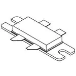
CASE 465M--01, STYLE 1
NI--780--4
MD7P19130HR3
CASE 465H--02, STYLE 1
NI--780S--4
MD7P19130HSR3
RFinA/VGSA 3
1 RFoutA/VDSA
RFinB/VGSB 4
2 RFoutB/VDSB
(Top View)
Figure 1. Pin Connections
Table 1. Maximum Ratings
Rating
Symbol
Value
Unit
Drain--Source Voltage
VDSS
--0.5, +65
Vdc
Gate--Source Voltage
VGS
--6.0, +10
Vdc
Operating Voltage
VDD
32, +0
Vdc
Storage Temperature Range
Tstg
-- 65 to +150
°C
TC
150
°C
TJ
225
°C
Case Operating Temperature
Operating Junction Temperature
(1,2)
1. Continuous use at maximum temperature will affect MTTF.
2. MTTF calculator available at http://www.freescale.com/rf. Select Software & Tools/Development Tools/Calculators to access
MTTF calculators by product.
© Freescale Semiconductor, Inc., 2008, 2010. All rights reserved.
RF Device Data
Freescale Semiconductor
MD7P19130HR3 MD7P19130HSR3
1
�Table 2. Thermal Characteristics
Characteristic
Value (1,2)
Symbol
Thermal Resistance, Junction to Case
Case Temperature 80°C, 130 W CW
Case Temperature 75°C, 40 W CW
RθJC
Unit
°C/W
0.31
0.36
Table 3. ESD Protection Characteristics
Test Methodology
Class
Human Body Model (per JESD22--A114)
1C (Minimum)
Machine Model (per EIA/JESD22--A115)
A (Minimum)
Charge Device Model (per JESD22--C101)
IV (Minimum)
Table 4. Electrical Characteristics (TA = 25°C unless otherwise noted)
Symbol
Min
Typ
Max
Unit
Zero Gate Voltage Drain Leakage Current
(VDS = 65 Vdc, VGS = 0 Vdc)
IDSS
—
—
10
μAdc
Zero Gate Voltage Drain Leakage Current
(VDS = 28 Vdc, VGS = 0 Vdc)
IDSS
—
—
1
μAdc
Gate--Source Leakage Current
(VGS = 5 Vdc, VDS = 0 Vdc)
IGSS
—
—
1
μAdc
Gate Threshold Voltage
(VDS = 10 Vdc, ID = 316 μAdc)
VGS(th)
1.2
2
2.7
Vdc
Gate Quiescent Voltage
(VDD = 28 Vdc, ID = 1250 mAdc, Measured in Functional Test)
VGS(Q)
1.9
2.7
3.4
Vdc
Drain--Source On--Voltage
(VGS = 10 Vdc, ID = 3.16 Adc)
VDS(on)
0.1
0.2
0.3
Vdc
Reverse Transfer Capacitance
(VDS = 28 Vdc ± 30 mV(rms)ac @ 1 MHz, VGS = 0 Vdc)
Crss
—
1.2
—
pF
Output Capacitance
(VDS = 28 Vdc ± 30 mV(rms)ac @ 1 MHz, VGS = 0 Vdc)
Coss
—
586
—
pF
Input Capacitance
(VDS = 28 Vdc, VGS = 0 Vdc ± 30 mV(rms)ac @ 1 MHz)
Ciss
—
348
—
pF
Characteristic
Off Characteristics
(3)
On Characteristics (3)
Dynamic Characteristics (3,4)
Functional Tests (3) (In Freescale Test Fixture, 50 ohm system) VDD = 28 Vdc, IDQ = 1250 mA, Pout = 40 W Avg., f = 1987.5 MHz,
Single--Carrier W--CDMA, IQ Magnitude Clipping, Input Signal PAR = 7.5 dB @ 0.01% Probability on CCDF. ACPR measured in 3.84 MHz
Channel Bandwidth @ ±5 MHz Offset.
Power Gain
Gps
18.5
20
21.5
dB
Drain Efficiency
ηD
27
30
—
%
Output Peak--to--Average Ratio @ 0.01% Probability on CCDF
Adjacent Channel Power Ratio
Input Return Loss
PAR
5.6
6
—
dB
ACPR
—
--36
--32.5
dBc
IRL
—
--16
--7
dB
1. MTTF calculator available at http://www.freescale.com/rf. Select Software & Tools/Development Tools/Calculators to access
MTTF calculators by product.
2. Refer to AN1955, Thermal Measurement Methodology of RF Power Amplifiers. Go to http://www.freescale.com/rf.
Select Documentation/Application Notes -- AN1955.
3. Measurement made with device in single--ended configuration.
4. Part internally matched both on input and output.
(continued)
MD7P19130HR3 MD7P19130HSR3
2
RF Device Data
Freescale Semiconductor
�Table 4. Electrical Characteristics (TA = 25°C unless otherwise noted) (continued)
Characteristic
Symbol
Min
Typ
Max
Unit
Typical Performances (In Freescale Test Fixture, 50 ohm system) VDD = 28 Vdc, IDQ = 1250 mA, 1930--1990 MHz Bandwidth
Pout @ 1 dB Compression Point, CW
P1dB
—
130
—
W
Gain Flatness in 60 MHz Bandwidth @ Pout = 40 W Avg.
GF
—
0.3
—
dB
Average Deviation from Linear Phase in 60 MHz Bandwidth
@ Pout = 130 W CW
Φ
—
0.5
—
°
Delay
—
2.3
—
ns
Part--to--Part Insertion Phase Variation @ Pout = 130 W CW,
f = 1960 MHz, Six Sigma Window
∆Φ
—
80
—
°
Gain Variation over Temperature
(--30°C to +85°C)
∆G
—
0.016
—
dB/°C
∆P1dB
—
0.01
—
dB/°C
Average Group Delay @ Pout = 130 W CW, f = 1960 MHz
Output Power Variation over Temperature
(--30°C to +85°C)
MD7P19130HR3 MD7P19130HSR3
RF Device Data
Freescale Semiconductor
3
�VBIAS
B1
+
+
C2
C1
C3
C4
R1
C7
C6
RF
INPUT
Z8
Z9
Z10
Z13
Z15
Z16
Z2
Z3
Z4
Z5
C10
C11
C12
Z17
Z18
Z12
Z19
Z1
C8
Z14
Z11
Z7
VSUPPLY
+
+
Z6
Z20
Z21
Z22
Z23
Z24
Z25
Z26
RF
OUTPUT
DUT
C9
C5
Z1
Z2
Z3
Z4
Z5
Z6
Z7
Z8
Z9
Z10
Z11
Z12
Z13
Z14
0.582″ x 0.110″ Microstrip
0.140″ x 0.284″ Microstrip
0.066″ x 0.080″ Microstrip
0.127″ x 0.080″ Microstrip
0.042″ x 0.237″ Microstrip
0.095″ x 0.375″ Microstrip
0.330″ x 0.320″ Microstrip
0.438″ x 0.530″ Microstrip
0.311″ x 0.741″ Microstrip
0.025″ x 0.814″ Microstrip
0.049″ x 0.254″ Microstrip
0.078″ x 0.814″ Microstrip
0.134″ x 0.957″ Microstrip
0.150″ x 0.276″ Microstrip
Z15
Z16
Z17
Z18
Z19
Z20
Z21
Z22
Z23
Z24
Z25
Z26
PCB
0.203″ x 0.957″ Microstrip
0.271″ x 0.930″ Microstrip
0.010″ x 0.540″ Microstrip
0.042″ x 0.205″ Microstrip
0.471″ x 0.080″ Microstrip
0.024″ x 0.241″ Microstrip
0.057″ x 0.349″ Microstrip
0.781″ x 0.311″ Microstrip
0.271″ x 0.080″ Microstrip
0.024″ x 0.095″ Microstrip
0.134″ x 0.190″ Microstrip
0.511″ x 0.080″ Microstrip
Arlon CuClad 250GX--0300--55--22, 0.030″, εr = 2.55
Figure 2. MD7P19130HR3(HSR3) Test Circuit Schematic
Table 5. MD7P19130HR3(HSR3) Test Circuit Component Designations and Values
Part
Description
Part Number
Manufacturer
B1
Short Ferrite Bead
2743019447 ROP50
Fair--Rite
C1
47 μF, 50 V Electrolytic Capacitor
476KXM063M
Illinois Cap.
C2
100 μF, 50 V Electrolitic Capacitor
T491C105K050AT
Kemet
C3
1.0 μF Chip Capacitor
ATC100B102JT50XT
ATC
C4, C12
0.1 μF Chip Capacitors
CDR33BX104AKYS
Kemet
C5, C9
11 pF Chip Capacitors
ATC100B110JT500XT
ATC
C6
13 pF Chip Capacitor
ATC100B130JT500XT
ATC
C7
8.2 pF Chip Capacitor
ATC100B8R2JT500XT
ATC
C8
22 μF, 35 V Tantalum Capacitor
T491C226K035AT
Kemet
C10
470 μF, 63 V Electrolytic Capacitor
477KXM063M
Illinois Cap.
C11
10 μF, 50 V Chip Capacitor
GRM55DR61H106KA88B
Murata
R1
10 Ω, 1/4 W Chip Resistor
CRCW120610R0FKEA
Vishay
MD7P19130HR3 MD7P19130HSR3
4
RF Device Data
Freescale Semiconductor
�C2
C10
C7
C6
R1
C3 C4
B1
C12
C1
C11
C8
C5
CUT OUT AREA
C9
MD7P19130H/HS
Rev. 2
Figure 3. MD7P19130HR3(HSR3) Test Circuit Component Layout
Single--ended
λ
4
λ
Quadrature combined
4
λ
4
λ
λ
2
2
Doherty
Push--pull
Figure 4. Possible Circuit Topologies
MD7P19130HR3 MD7P19130HSR3
RF Device Data
Freescale Semiconductor
5
�32
Gps, POWER GAIN (dB)
21.5
21
20.5
Gps
20
26
3.84 MHz Channel Bandwidth, Input Signal
PAR = 7.5 dB @ 0.01% Probability (CCDF)
19.5
19
18.5 ACPR
18
17.5
1880
29
VDD = 28 Vdc, Pout = 40 W (Avg.)
IDQ = 1250 mA, Single--Carrier W--CDMA
--28
--4
--30
--8
--32
--34
--36
PARC
1900
IRL
1920
1940
1960
1980
2000
2020
--38
2040
--12
--16
--20
--24
0
--0.5
--1
--1.5
--2
PARC (dB)
35
IRL, INPUT RETURN LOSS (dB)
38
ηD
22
ACPR (dBc)
22.5
ηD, DRAIN
EFFICIENCY (%)
TYPICAL CHARACTERISTICS
--2.5
f, FREQUENCY (MHz)
Figure 5. Output Peak--to--Average Ratio Compression (PARC)
Broadband Performance @ Pout = 40 Watts Avg.
21.5
IDQ = 1875 mA
Gps, POWER GAIN (dB)
20.5
1562.5 mA
19.5
1250 mA
18.5
937.5 mA
17.5
VDD = 28 Vdc, f = 1960 MHz
CW Measurements
625 mA
16.5
10
1
200
100
Pout, OUTPUT POWER (WATTS) CW
Figure 6. CW Power Gain versus Output Power
19
18.5
18
17.5
0
--1
Gps
--1 dB = 33.42 W
--2 dB = 49.63 W
--2
ACPR
--5
20
30
40
50
45
--25
35
30
VDD = 28 Vdc, IDQ = 1250 mA
PARC
f = 1960 MHz, Single--Carrier W--CDMA
3.84 MHz Channel Bandwidth, Input Signal
PAR = 7.5 dB @ 0.01% Probability (CCDF)
--4
--20
40
--3 dB = 69.20 W
ηD
--3
50
60
70
80
90
100
110
--30
--35
--40
25
--45
20
--50
120
ACPR (dBc)
19.5
OUTPUT COMPRESSION AT THE 0.01%
PROBABILITY ON CCDF (dB)
Gps, POWER GAIN (dB)
20
1
ηD, DRAIN EFFICIENCY (%)
20.5
Pout, OUTPUT POWER (WATTS)
Figure 7. Output Peak--to--Average Ratio
Compression (PARC) versus Output Power
MD7P19130HR3 MD7P19130HSR3
6
RF Device Data
Freescale Semiconductor
�TYPICAL CHARACTERISTICS
23
50
--10
85°C
40
85°C
17 VDD = 28 Vdc, IDQ = 1250 mA, f = 1960 MHz
Single--Carrier W--CDMA, 3.84 MHz
Channel Bandwidth, Input Signal
15
PAR = 7.5 dB @ 0.01%
Probability (CCDF)
13
ACPR
ηD
30
--40°C
25°C
10
85°C
11
1
20
10
100
--20
--30
--40
ACPR (dBc)
Gps, POWER GAIN (dB)
25°C
25°C
19
0
ηD, DRAIN EFFICIENCY (%)
TC = --40°C
21
60
--40°C
Gps
--50
0
200
--60
Pout, OUTPUT POWER (WATTS) AVG.
Figure 8. Single--Carrier W--CDMA Power Gain, Drain
Efficiency and ACPR versus Output Power
S21
--5
S21 (dB)
--15
12
S11
--20
8
VDD = 28 Vdc
IDQ = 1250 mA
4
1650
1750
1850
S11 (dB)
--10
16
MTTF (HOURS)
20
0
1550
109
0
24
108
107
--25
1950
2050
2150
2250
f, FREQUENCY (MHz)
Figure 9. Broadband Frequency Response
--30
2350
106
90
110
130
150
170
190
210
230
250
TJ, JUNCTION TEMPERATURE (°C)
This above graph displays calculated MTTF in hours when the device
is operated at VDD = 28 Vdc, Pout = 40 W Avg., and ηD = 30%.
MTTF calculator available at http://www.freescale.com/rf. Select
Software & Tools/Development Tools/Calculators to access MTTF
calculators by product.
Figure 10. MTTF versus Junction Temperature
MD7P19130HR3 MD7P19130HSR3
RF Device Data
Freescale Semiconductor
7
�W--CDMA TEST SIGNAL
100
10
10
--10
--30
Input Signal
0.1
0.01
0
1
2
3
4
5
6
--40
--50
--60
W--CDMA. ACPR Measured in 3.84 MHz
Channel Bandwidth @ ±5 MHz Offset.
Input Signal PAR = 7.5 dB @ 0.01%
Probability on CCDF
0.001
0.0001
3.84 MHz
Channel BW
--20
1
(dB)
PROBABILITY (%)
0
+ACPR in 3.84 MHz
Integrated BW
--ACPR in 3.84 MHz
Integrated BW
--70
--80
7
8
9
PEAK--TO--AVERAGE (dB)
Figure 11. CCDF W--CDMA IQ Magnitude
Clipping, Single--Carrier Test Signal
10
--90
--100
--9
--7.2 --5.4
--3.6 --1.8
0
1.8
3.6
5.4
7.2
9
f, FREQUENCY (MHz)
Figure 12. Single--Carrier W--CDMA Spectrum
MD7P19130HR3 MD7P19130HSR3
8
RF Device Data
Freescale Semiconductor
�Zo = 10 Ω
Zsource
f = 1880 MHz
f = 2040 MHz
f = 2040 MHz
Zload
f = 1880 MHz
VDD = 28 Vdc, IDQ = 1250 mA, Pout = 40 W Avg.
f
MHz
Zsource
Ω
Zload
Ω
1880
7.37 + j1.00
1.84 -- j3.56
1900
7.33 + j0.96
1.78 -- j3.37
1920
7.27 + j0.93
1.72 -- j3.17
1940
7.19 + j0.90
1.64 -- j2.98
1960
7.07 + j0.89
1.55 -- j2.79
1980
6.93 + j0.97
1.48 -- j2.55
2000
6.89 + j1.04
1.46 -- j2.36
2020
6.83 + j1.07
1.44 -- j2.20
2040
6.75 + j1.12
1.40 -- j2.02
Zsource = Test circuit impedance as measured from
gate to ground.
Zload
= Test circuit impedance as measured
from drain to ground.
Output
Matching
Network
Device
Under
Test
Input
Matching
Network
Z
source
Z
load
Figure 13. Series Equivalent Source and Load Impedance
MD7P19130HR3 MD7P19130HSR3
RF Device Data
Freescale Semiconductor
9
�Pout, OUTPUT POWER (dBm)
ALTERNATIVE PEAK TUNE LOAD PULL CHARACTERISTICS
57
56
55
54
53
52
51
50
49
48
47
46
45
44
43
Ideal
P3dB = 53.48 dBm (223 W)
P1dB = 52.67 dBm (185 W)
Actual
VDD = 28 Vdc, IDQ = 1250 mA, Pulsed CW
10 μsec(on), 10% Duty Cycle, f = 1960 MHz
24 25
26 27 28 29 30 31 32 33 34 35 36 37 38
Pin, INPUT POWER (dBm)
NOTE: Load Pull Test Fixture Tuned for Peak P1dB Output Power @ 28 V
Test Impedances per Compression Level
P1dB
Zsource
Ω
Zload
Ω
7.15 -- j1.86
0.84 -- j2.99
Figure 14. Pulsed CW Output Power
versus Input Power @ 28 V
MD7P19130HR3 MD7P19130HSR3
10
RF Device Data
Freescale Semiconductor
�PACKAGE DIMENSIONS
MD7P19130HR3 MD7P19130HSR3
RF Device Data
Freescale Semiconductor
11
�MD7P19130HR3 MD7P19130HSR3
12
RF Device Data
Freescale Semiconductor
�MD7P19130HR3 MD7P19130HSR3
RF Device Data
Freescale Semiconductor
13
�MD7P19130HR3 MD7P19130HSR3
14
RF Device Data
Freescale Semiconductor
�PRODUCT DOCUMENTATION AND SOFTWARE
Refer to the following documents to aid your design process.
Application Notes
• AN1955: Thermal Measurement Methodology of RF Power Amplifiers
Engineering Bulletins
• EB212: Using Data Sheet Impedances for RF LDMOS Devices
Software
• Electromigration MTTF Calculator
• RF High Power Model
For Software, do a Part Number search at http://www.freescale.com, and select the “Part Number” link. Go to the Software &
Tools tab on the part’s Product Summary page to download the respective tool.
REVISION HISTORY
The following table summarizes revisions to this document.
Revision
Date
Description
0
May 2008
• Initial Release of Data Sheet
1
Dec. 2008
• Corrected the pin order in Fig. 1, Pin Connections, to match the Mechanical Outline pin order, p. 1
2
Aug. 2010
• Modified data sheet to reflect RF Test Reduction described in Product and Process Change Notification
number, PCN13628, p. 1, 2
• Updated Fig. 14, CCDF W--CDMA IQ Magnitude Clipping, Single--Carrier Test Signal, to better represent
production test signal, p. 8
• Updated Fig. 15, Single--Carrier W--CDMA Spectrum, to better represent production test signal, p. 8
• Added Electromigration MTTF Calculator and RF High Power Model availability to Product Software, p.
15
MD7P19130HR3 MD7P19130HSR3
RF Device Data
Freescale Semiconductor
15
�How to Reach Us:
Home Page:
www.freescale.com
Web Support:
http://www.freescale.com/support
USA/Europe or Locations Not Listed:
Freescale Semiconductor, Inc.
Technical Information Center, EL516
2100 East Elliot Road
Tempe, Arizona 85284
1--800--521--6274 or +1--480--768--2130
www.freescale.com/support
Europe, Middle East, and Africa:
Freescale Halbleiter Deutschland GmbH
Technical Information Center
Schatzbogen 7
81829 Muenchen, Germany
+44 1296 380 456 (English)
+46 8 52200080 (English)
+49 89 92103 559 (German)
+33 1 69 35 48 48 (French)
www.freescale.com/support
Japan:
Freescale Semiconductor Japan Ltd.
Headquarters
ARCO Tower 15F
1--8--1, Shimo--Meguro, Meguro--ku,
Tokyo 153--0064
Japan
0120 191014 or +81 3 5437 9125
support.japan@freescale.com
Asia/Pacific:
Freescale Semiconductor China Ltd.
Exchange Building 23F
No. 118 Jianguo Road
Chaoyang District
Beijing 100022
China
+86 10 5879 8000
support.asia@freescale.com
For Literature Requests Only:
Freescale Semiconductor Literature Distribution Center
1--800--441--2447 or +1--303--675--2140
Fax: +1--303--675--2150
LDCForFreescaleSemiconductor@hibbertgroup.com
Information in this document is provided solely to enable system and software
implementers to use Freescale Semiconductor products. There are no express or
implied copyright licenses granted hereunder to design or fabricate any integrated
circuits or integrated circuits based on the information in this document.
Freescale Semiconductor reserves the right to make changes without further notice to
any products herein. Freescale Semiconductor makes no warranty, representation or
guarantee regarding the suitability of its products for any particular purpose, nor does
Freescale Semiconductor assume any liability arising out of the application or use of
any product or circuit, and specifically disclaims any and all liability, including without
limitation consequential or incidental damages. “Typical” parameters that may be
provided in Freescale Semiconductor data sheets and/or specifications can and do
vary in different applications and actual performance may vary over time. All operating
parameters, including “Typicals”, must be validated for each customer application by
customer’s technical experts. Freescale Semiconductor does not convey any license
under its patent rights nor the rights of others. Freescale Semiconductor products are
not designed, intended, or authorized for use as components in systems intended for
surgical implant into the body, or other applications intended to support or sustain life,
or for any other application in which the failure of the Freescale Semiconductor product
could create a situation where personal injury or death may occur. Should Buyer
purchase or use Freescale Semiconductor products for any such unintended or
unauthorized application, Buyer shall indemnify and hold Freescale Semiconductor
and its officers, employees, subsidiaries, affiliates, and distributors harmless against all
claims, costs, damages, and expenses, and reasonable attorney fees arising out of,
directly or indirectly, any claim of personal injury or death associated with such
unintended or unauthorized use, even if such claim alleges that Freescale
Semiconductor was negligent regarding the design or manufacture of the part.
Freescalet and the Freescale logo are trademarks of Freescale Semiconductor, Inc.
All other product or service names are the property of their respective owners.
© Freescale Semiconductor, Inc. 2008, 2010. All rights reserved.
MD7P19130HR3 MD7P19130HSR3
Document Number: MD7P19130H
Rev. 2, 8/2010
16
RF Device Data
Freescale Semiconductor
�