Freescale Semiconductor
Technical Data
Document Number: MD8IC970N
Rev. 2, 5/2011
RF LDMOS Wideband Integrated
Power Amplifiers
The MD8IC970N wideband integrated circuit is designed with on--chip
prematching that makes it usable from 136 to 940 MHz. This multi--stage
structure is rated for 26 to 32 Volt operation and covers all typical base station
modulation formats. This device has a 2--stage design with off--chip matching
for the input, interstage and output networks to cover the desired frequency
sub--band.
• Typical Two--Tone Performance: VDD1 = 28 Volts, VDD2 = 25 Volts,
IDQ1(A+B) = 60 mA, IDQ2(A+B) = 550 mA, Pout = 35 Watts Avg.
Frequency
Gps
(dB)
PAE
(%)
IMD
(dBc)
850 MHz
30.6
40.1
--30.5
900 MHz
31.9
42.4
--31.0
940 MHz
32.6
42.1
--31.3
MD8IC970NR1
MD8IC970GNR1
850--940 MHz, 35 W AVG., 28 V
RF LDMOS WIDEBAND
INTEGRATED POWER AMPLIFIERS
• Capable of Handling 10:1 VSWR, @ 32 Vdc, 940 MHz, 137 Watts CW
Output Power (3 dB Input Overdrive from Rated Pout), Designed for
Enhanced Ruggedness
• Typical Pout @ 1 dB Compression Point ≃ 79 Watts CW
Features
• Characterized with Series Equivalent Large--Signal Impedance Parameters
and Common Source S--Parameters
• On--Chip Prematching. On--Chip Stabilization.
• Integrated Quiescent Current Temperature Compensation with
Enable/Disable Function (1)
• Integrated ESD Protection
• 225°C Capable Plastic Package
• RoHS Compliant
• In Tape and Reel. R1 Suffix = 500 Units, 44 mm Tape Width, 13 inch Reel.
RFin2A
RFout1A/VD1A
VG1A
RFin1A
RFout2A/VD2A
VG2A
Quiescent Current
Temperature Compensation (1)
RFin2B
RFout1B/VD1B
VG2B
RFout2B/VD2B
RFin1B
VG1B
Quiescent Current
Temperature Compensation (1)
Figure 1. Functional Block Diagram
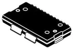
CASE 1866--02
TO--270 WBL--16
PLASTIC
MD8IC970NR1
CASE 1867--02
TO--270 WBL--16 GULL
PLASTIC
MD8IC970GNR1
RFin2A
RFout1A/VD1A
GND
GND
VG1A
RFin1A
VG2A
VG2B
RFin1B
VG1B
GND
GND
RFout1B/VD1B
RFin2B
1
2
3
4
5
6
7
8
9
10
11
12
13
14
16
RFout2A/
VD2A
15
RFout2B/
VD2B
(Top View)
Note: Exposed backside of the package is
the source terminal for the transistors.
Figure 2. Pin Connections
1. Refer to AN1977, Quiescent Current Thermal Tracking Circuit in the RF Integrated Circuit Family and to AN1987, Quiescent Current Control
for the RF Integrated Circuit Device Family. Go to http://www.freescale.com/rf. Select Documentation/Application Notes -- AN1977 or AN1987.
© Freescale Semiconductor, Inc., 2011. All rights reserved.
RF Device Data
Freescale Semiconductor
MD8IC970NR1 MD8IC970GNR1
1
�Table 1. Maximum Ratings
Rating
Symbol
Value
Unit
Drain--Source Voltage
VDSS
--0.5, +70
Vdc
Gate--Source Voltage
VGS
--0.5, +10
Vdc
Operating Voltage
VDD
32, +0
Vdc
Storage Temperature Range
Tstg
--65 to +150
°C
Case Operating Temperature
TC
150
°C
Operating Junction Temperature (1,2)
TJ
225
°C
Input Power
Pin
30
dBm
Symbol
Value (2,3)
Unit
Table 2. Thermal Characteristics
Characteristic
Final Application
RθJC
Thermal Resistance, Junction to Case
Case Temperature 80°C, 35 W Avg. Two--Tone
Stage 1, 28 Vdc, IDQ1(A+B) = 60 mA, f1 = 939.9 MHz, f2 = 940.1 MHz
Stage 2, 25 Vdc, IDQ2(A+B) = 550 mA, f1 = 939.9 MHz, f2 = 940.1 MHz
°C/W
2.9
0.6
Table 3. ESD Protection Characteristics
Test Methodology
Class
Human Body Model (per JESD22--A114)
1A (Minimum)
Machine Model (per EIA/JESD22--A115)
A (Minimum)
Charge Device Model (per JESD22--C101)
I (Minimum)
Table 4. Moisture Sensitivity Level
Test Methodology
Per JESD22--A113, IPC/JEDEC J--STD--020
Rating
Package Peak Temperature
Unit
3
260
°C
Table 5. Electrical Characteristics (TA = 25°C unless otherwise noted)
Symbol
Min
Typ
Max
Unit
Zero Gate Voltage Drain Leakage Current
(VDS = 70 Vdc, VGS = 0 Vdc)
IDSS
—
—
10
μAdc
Zero Gate Voltage Drain Leakage Current
(VDS = 28 Vdc, VGS = 0 Vdc)
IDSS
—
—
1
μAdc
Gate--Source Leakage Current
(VGS = 1.5 Vdc, VDS = 0 Vdc)
IGSS
—
—
1
μAdc
Gate Threshold Voltage
(VDS = 10 Vdc, ID = 40 μAdc)
VGS(th)
1.2
2.0
2.7
Vdc
Gate Quiescent Voltage
(VDS = 28 Vdc, IDQ1(A+B) = 60 mAdc)
VGS(Q)
—
3.1
—
Vdc
Fixture Gate Quiescent Voltage
(VDD1 = 28 Vdc, IDQ1(A+B) = 60 mAdc, Measured in Functional Test)
VGG(Q)
9.0
10.0
11.0
Vdc
Characteristic
Stage 1 — Off Characteristics (4)
Stage 1 — On Characteristics (4)
1. Continuous use at maximum temperature will affect MTTF.
2. MTTF calculator available at http://www.freescale.com/rf. Select Software & Tools/Development Tools/Calculators to access MTTF
calculators by product.
3. Refer to AN1955, Thermal Measurement Methodology of RF Power Amplifiers. Go to http://www.freescale.com/rf.
Select Documentation/Application Notes -- AN1955.
4. Side A and Side B are tied together for this measurement.
(continued)
MD8IC970NR1 MD8IC970GNR1
2
RF Device Data
Freescale Semiconductor
�Table 5. Electrical Characteristics (TA = 25°C unless otherwise noted) (continued)
Symbol
Min
Typ
Max
Unit
Zero Gate Voltage Drain Leakage Current
(VDS = 70 Vdc, VGS = 0 Vdc)
IDSS
—
—
10
μAdc
Zero Gate Voltage Drain Leakage Current
(VDS = 28 Vdc, VGS = 0 Vdc)
IDSS
—
—
1
μAdc
Gate--Source Leakage Current
(VGS = 1.5 Vdc, VDS = 0 Vdc)
IGSS
—
—
1
μAdc
Gate Threshold Voltage
(VDS = 10 Vdc, ID = 320 μAdc)
VGS(th)
1.2
2.0
2.7
Vdc
Gate Quiescent Voltage
(VDS = 25 Vdc, IDQ2(A+B) = 550 mAdc)
VGS(Q)
—
3.1
—
Vdc
Fixture Gate Quiescent Voltage
(VDD2 = 25 Vdc, IDQ2(A+B) = 550 mAdc, Measured in Functional Test)
VGG(Q)
7.6
8.6
9.6
Vdc
Drain--Source On--Voltage
(VGS = 10 Vdc, ID = 3.2 Adc)
VDS(on)
0.1
0.48
1.2
Vdc
Characteristic
Stage 2 — Off Characteristics (1)
Stage 2 — On Characteristics (1)
Functional Tests (1,2) (In Freescale Test Fixture, 50 ohm system) VDD1 = 28 Vdc, VDD2 = 25 Vdc, Pout = 35 W Avg., IDQ1(A+B) = 60 mA,
IDQ2(A+B) = 550 mA, f1 = 939.9 MHz, f2 = 940.1 MHz
Power Gain
Gps
31.5
32.6
36.5
dB
Power Added Efficiency
PAE
40.5
42.1
—
%
IMD
—
--31.3
--29.0
dB
Intermodulation Distortion
(1) (In
Typical Broadband Performance
IDQ1(A+B) = 60 mA, IDQ2(A+B) = 550 mA
Freescale Test Fixture, 50 ohm system) VDD1 = 28 Vdc, VDD2 = 25 Vdc, Pout = 35 W Avg.,
Frequency
Gps
(dB)
PAE
(%)
IMD
(dBc)
850 MHz
30.6
40.1
--30.5
900 MHz
31.9
42.4
--31.0
940 MHz
32.6
42.1
--31.3
Typical Performances (1) (In Freescale Test Fixture, 50 ohm system) VDD1 = 28 Vdc, VDD2 = 25 Vdc, IDQ1(A+B) = 60 mA,
IDQ2(A+B) = 550 mA, 850--940 MHz Bandwidth
Characteristic
Pout @ 1 dB Compression Point, CW
Symbol
Min
Typ
Max
Unit
P1dB
—
79
—
W
—
22
—
IMD Symmetry @ 71 W PEP, Pout where IMD Third Order
Intermodulation 30 dBc
(Delta IMD Third Order Intermodulation between Upper and Lower
Sidebands > 2 dB)
IMDsym
VBW Resonance Point
(IMD Third Order Intermodulation Inflection Point)
VBWres
—
50
—
MHz
∆IQT
—
—
5.03
4.61
—
—
%
Gain Flatness in 90 MHz Bandwidth @ Pout = 35 W Avg.
GF
—
1.2
—
dB
Gain Variation over Temperature
(--30°C to +85°C)
∆G
—
0.03
—
dB/°C
∆P1dB
—
0.005
—
dB/°C
Quiescent Current Accuracy over Temperature
with 8.25 kΩ Gate Feed Resistors (--30 to 85°C) (3)
Output Power Variation over Temperature
(--30°C to +85°C)
Stage 1
Stage 2
MHz
1. Side A and Side B are tied together for this measurement.
2. Part internally matched both on input and output.
3. Refer to AN1977, Quiescent Current Thermal Tracking Circuit in the RF Integrated Circuit Family and to AN1987, Quiescent Current Control
for the RF Integrated Circuit Device Family. Go to http://www.freescale.com/rf. Select Documentation/Application Notes -- AN1977 or
AN1987.
MD8IC970NR1 MD8IC970GNR1
RF Device Data
Freescale Semiconductor
3
�VDD1A
R2
C1
VGG1A C9
C5
Z1
L3
C17
C2
C6
VGG1B C10
VDD1B R3
C14
C8
C27
R7
L4
VDD2A
C19
R6
C18
R8
C35
R4
C16
C12
C4
VGG2B
C7
C13
C11
C15
C3
R1
L5
L1
C21
C22
C20
R5
L2
CUT OUT AREA
VGG2A
C23
C29
C25
C31
C26
C32
C24
C30
C33
Z2
R10
C34
VDD2B
C28
C36
L6
R9
MD8IC970N
Rev. 1
Figure 3. MD8IC970NR1(GNR1) Test Circuit Component Layout
Table 6. MD8IC970NR1(GNR1) Test Circuit Component Designations and Values
Part
Description
Part Number
Manufacturer
C1, C2, C35, C36
10 μF, 50 V Chip Capacitors
GRM55DR61H106KA88L
Murata
C3, C4, C9, C10
1 μF, 50 V Chip Capacitors
GRM31MR71H105KA88L
Murata
C5, C6
3.3 pF Chip Capacitors
ATC600F3R3BT250XT
ATC
C7, C8, C27, C28, C33, C34
39 pF Chip Capacitors
ATC600F390JT250XT
ATC
C11, C12
47 pF Chip Capacitors
ATC600S470JT250XT
ATC
C13, C14
4.7 pF Chip Capacitors
ATC600S4R7JT250XT
ATC
C15, C16, C19, C20
0.1 μF, 50 V Chip Capacitors
GRM188R71C104K01D
Murata
C17, C18
5.6 pF Chip Capacitors
ATC600S5R6JT250XT
ATC
C21, C22
15 pF Chip Capacitors
ATC600F150JT250XT
ATC
C23, C24, C25, C26
4.7 pF Chip Capacitors
ATC600F4R7BT250XT
ATC
C29. C30, C31, C32
2.7 pF Chip Capacitors
ATC600F2R7BT250XT
ATC
L1, L2, L5, L6
5.0 nH 2 Turn Inductors
A02TKLC
Coilcraft
L3, L4
2.8 nH Chip Inductors
0805CS--020XJLC
Coilcraft
R1
51 Ω, 1/8 W Chip Resistor
SG73P2ATTD51R0F
KOA Speer
R2, R3, R8, R9
10 Ω, 1/8 W Chip Resistors
RK73H2ATTD10R0F
KOA Speer
R4, R5, R6, R7
8.25 kΩ, 1/10 W Chip Resistors
RK73H1JTTD8251F
KOA Speer
R10
50 Ω, 10 W SM Chip Power Resistor
81A7031--50--5F
Florida RF Labs
Z1, Z2
900 MHz Band, 90°, 3 dB Chip Hybrid Couplers
GSC362--HYB0900
Soshin
PCB
0.030″, εr = 3.66
RO4350B
Rogers
MD8IC970NR1 MD8IC970GNR1
4
RF Device Data
Freescale Semiconductor
�TYPICAL CHARACTERISTICS
Gps, POWER GAIN (dB)
PAE, POWER ADDED
EFFICIENCY (%)
44
PAE
35
42
34
40
33
38
32
Gps
31
--27
VDD1 = 28 Vdc, VDD2 = 25 Vdc, IDQ1(A+B) = 60 mA
--28
IDQ2(A+B) = 550 mA, Pout = 35 W (Avg.)
--29
200 kHz Tone Spacing
30
29
28
36
--30
IMD
27
26
820
--31
--32
840
860
880
900
920
940
960
980
IMD, INTERMODULATION
DISTORTION (dBc)
36
f, FREQUENCY (MHz)
IMD, INTERMODULATION DISTORTION (dBc)
Figure 4. Two--Tone Broadband Performance
@ Pout = 35 Watts Avg.
--10
VDD1 = 28 Vdc, VDD2 = 25 Vdc, Pout = 71 W (PEP)
IDQ1(A+B) = 60 mA, IDQ2(A+B) = 550 mA
Two--Tone Measurements
(f1 + f2)/2 = Center Frequency of 900 MHz
--20
IM3--U
--30
IM3--L
IM5--U
--40
IM5--L
IM7--U
--50
--60
IM7--L
1
10
100
TWO--TONE SPACING (MHz)
Figure 5. Intermodulation Distortion Products
versus Two--Tone Spacing
PAE
Gps
33
50
40
IMD
32
30
31
20
30
10
29
10
0
20
30
40
50
--10
--20
--30
--40
--50
--60
IMD, INTERMODULATION DISTORTION (dBc)
Gps, POWER GAIN (dB)
34
0
60
VDD1 = 28 Vdc, VDD2 = 25 Vdc, IDQ1(A+B) = 60 mA
IDQ2(A+B) = 550 mA, f1 = 939.9 MHz, f2 = 940.1 MHz
PAE, POWER ADDED EFFICIENCY (%)
35
60
Pout, OUTPUT POWER (WATTS)
Figure 6. Power Gain, Power Added Efficiency and
Intermodulation Distortion Products versus
Average Output Power
MD8IC970NR1 MD8IC970GNR1
RF Device Data
Freescale Semiconductor
5
�34
Gps, POWER GAIN (dB)
60
VDD1 = 28 Vdc, VDD2 = 25 Vdc, IDQ1(A+B) = 60 mA
IDQ2(A+B) = 550 mA, 200 kHz Tone Spacing
900 MHz
32
Gps
30
50
940 MHz
40
850 MHz
30
IMD
28
20
940 MHz
26
900 MHz
PAE
10
850 MHz
0
100
24
1
--10
PAE, POWER ADDED EFFICIENCY (%)
36
10
--20
--30
--40
--50
--60
--70
IMD, INTERMODULATION DISTORTION (dBc)
TYPICAL CHARACTERISTICS
Pout, OUTPUT POWER (WATTS) AVG.
Figure 7. Power Gain, Power Added Efficiency and Intermodulation
Distortion Products versus Output Power
36
34
VDD1 = 28 Vdc, VDD2 = 25 Vdc
Pin = 0 dBm, IDQ1(A+B) = 60 mA
IDQ2(A+B) = 550 mA
Gain
GAIN (dB)
32
30
28
26
24
700
750
800
850
900
950
1000
1050
1100
f, FREQUENCY (MHz)
Figure 8. Broadband Frequency Response
MD8IC970NR1 MD8IC970GNR1
6
RF Device Data
Freescale Semiconductor
�VDD1 = 28 Vdc, IDQ1(A) = 30 mA
Zin
f
MHz
Zin
Ω
Zload
Ω
f
MHz
Zin
Ω
Zload
Ω
820
18.4 -- j13.0
11.3 + j20.0
330
31.2 -- j21.5
16.2 + j57.8
840
18.8 -- j12.7
11.7 + j21.9
350
33.6 -- j18.7
24.2 + j59.6
860
19.1 -- j12.9
12.1 + j23.4
370
35.8 -- j18.8
29.8 + j55.6
880
19.1 -- j13.2
12.5 + j24.5
390
36.4 -- j19.6
29.0 + j52.8
900
18.7 -- j13.6
12.7 + j25.1
410
37.0 -- j20.1
27.8 + j54.7
920
18.0 -- j13.9
12.5 + j25.6
430
37.7 -- j21.7
30.2 + j58.5
940
17.2 -- j14.2
11.8 + j26.0
450
36.2 -- j24.8
38.8 + j59.1
960
16.1 -- j14.3
10.9 + j26.6
980
14.6 -- j14.3
9.6 + j27.4
Zin
= Device input impedance as measured from
gate to ground.
Zload = Test circuit impedance as measured from
drain to ground.
= Device input impedance as measured from
gate to ground.
Zload = Test circuit impedance as measured from
drain to ground.
Zin
f
MHz
Zin
Ω
Zload
Ω
120
42.7 -- j27.4
47.3 + j80.0
130
40.0 -- j22.5
61.4 + j93.3
140
40.2 -- j16.0
84.0 + j104.2
150
43.8 -- j13.3
114.5 + j107.2
160
47.8 -- j10.0
147.2 + j98.5
170
51.5 -- j10.0
179.4 + j81.3
180
54.9 -- j10.6
215.9 + j53.3
190
58.2 -- j12.9
256.6 -- j7.6
200
59.6 -- j16.9
233.3 -- j109.9
= Device input impedance as measured from
gate to ground.
Zload = Test circuit impedance as measured from
drain to ground.
Output
Matching
Network
Device
Under Test
Z
in
Z
load
Figure 9. Series Equivalent Input and Load Impedance — Stage 1
NOTE: Measurement made on a per side basis.
MD8IC970NR1 MD8IC970GNR1
RF Device Data
Freescale Semiconductor
7
�VDD2 = 25 Vdc, IDQ2(A) = 275 mA, Pout = 17.5 Watts Avg.
Zin
f
MHz
Zin
Ω
Zload
Ω
f
MHz
Zin
Ω
Zload
Ω
820
9.49 + j10.2
3.19 + j1.99
330
5.78 + j3.02
5.53 + j1.53
840
10.3 + j10.3
3.29 + j2.11
350
5.73 + j3.40
6.27 + j1.77
860
11.2 + j10.2
3.39 + j2.18
370
5.66 + j3.89
6.95 + j1.55
880
12.2 + j9.89
3.45 + j2.20
390
5.63 + j4.34
7.18 + j0.90
900
13.1 + j9.34
3.46 + j2.16
410
5.60 + j4.75
6.67 + j0.22
920
14.0 + j8.53
3.40 + j2.08
430
5.53 + j5.06
5.61 + j0.05
940
14.6 + j7.51
3.24 + j2.00
450
5.38 + j5.32
4.45 + j0.57
960
15.1 + j6.28
2.98 + j1.96
980
15.2 + j4.87
2.66 + j1.99
Zin
= Device input impedance as measured from
gate to ground.
Zload = Test circuit impedance as measured from
drain to ground.
= Device input impedance as measured from
gate to ground.
Zload = Test circuit impedance as measured from
drain to ground.
Zin
f
MHz
Zin
Ω
Zload
Ω
120
5.47 -- j0.60
5.74 + j2.70
130
5.46 -- j0.36
6.36 + j1.97
140
5.47 -- j0.13
6.21 + j1.37
150
5.47 + j0.11
5.95 + j1.37
160
5.46 + j0.35
6.09 + j1.63
170
5.43 + j0.56
6.59 + j1.58
180
5.42 + j0.75
6.70 + j0.92
190
5.49 + j0.93
5.73 + j0.82
200
5.42 + j1.05
4.83 + j2.57
= Device input impedance as measured from
gate to ground.
Zload = Test circuit impedance as measured from
drain to ground.
Output
Matching
Network
Device
Under Test
Z
in
Z
load
Figure 10. Series Equivalent Input and Load Impedance — Stage 2
NOTE: Measurement made on a per side basis.
MD8IC970NR1 MD8IC970GNR1
8
RF Device Data
Freescale Semiconductor
�ALTERNATIVE PEAK TUNE LOAD PULL CHARACTERISTICS — STAGE 2
VDD2 = 25 Vdc, IDQ2 = 300 mA, CW
VDD2 = 25 Vdc, IDQ2 = 300 mA, CW
Max Pout
P1dB
Max Eff.
Zsource
Ω
Zload (1)
Ω
P1dB
%
f
MHz
Zsource
Ω
Zload (1)
Ω
dBm
W
f
MHz
850
10.9 + j10.2
3.34 + j2.16
47.1
51
850
10.9 + j10.2
3.36 + j3.93
66.2
940
14.6 + j7.51
3.24 + j2.00
46.8
48
940
14.6 + j7.51
2.95 + j3.66
62.1
(1) Load impedance for optimum P1dB power.
(1) Load impedance for optimum P1dB efficiency.
Zsource = Impedance as measured from gate contact to ground.
Zload = Impedance as measured from drain contact to ground.
Zsource = Impedance as measured from gate contact to ground.
Zload = Impedance as measured from drain contact to ground.
Input
Load Pull
Tuner
Z
Z
source
Input
Load Pull
Tuner
Output
Load Pull
Tuner
Device
Under
Test
Z
load
Output
Load Pull
Tuner
Device
Under
Test
Z
source
load
Figure 11. Single Side Load Pull Performance —
Maximum P1dB Tuning
Figure 12. Single Side Load Pull Performance —
Maximum Efficiency Tuning
VDD2 = 25 Vdc, IDQ2 = 300 mA, CW
VDD2 = 25 Vdc, IDQ2 = 300 mA, CW
Max Pout
f
MHz
Zload (1)
Ω
Zsource
Ω
P1dB
dBm
W
430
5.53 + j5.06
5.61 + j0.05
46.8
(1) Load impedance for optimum P1dB power.
48
Zsource = Impedance as measured from gate contact to ground.
Zload = Impedance as measured from drain contact to ground.
Input
Load Pull
Tuner
Output
Load Pull
Tuner
Device
Under
Test
Z
source
Z
load
Figure 13. Single Side Load Pull Performance —
Maximum P1dB Tuning
Max Eff.
f
MHz
Zsource
Ω
430
5.53 + j5.06
Zload
Ω
(1)
5.96 + j2.65
P1dB
%
66.1
(1) Load impedance for optimum P1dB efficiency.
Zsource = Impedance as measured from gate contact to ground.
Zload = Impedance as measured from drain contact to ground.
Input
Load Pull
Tuner
Output
Load Pull
Tuner
Device
Under
Test
Z
source
Z
load
Figure 14. Single Side Load Pull Performance —
Maximum Efficiency Tuning
MD8IC970NR1 MD8IC970GNR1
RF Device Data
Freescale Semiconductor
9
�PACKAGE DIMENSIONS
MD8IC970NR1 MD8IC970GNR1
10
RF Device Data
Freescale Semiconductor
�MD8IC970NR1 MD8IC970GNR1
RF Device Data
Freescale Semiconductor
11
�MD8IC970NR1 MD8IC970GNR1
12
RF Device Data
Freescale Semiconductor
�MD8IC970NR1 MD8IC970GNR1
RF Device Data
Freescale Semiconductor
13
�MD8IC970NR1 MD8IC970GNR1
14
RF Device Data
Freescale Semiconductor
�MD8IC970NR1 MD8IC970GNR1
RF Device Data
Freescale Semiconductor
15
�PRODUCT DOCUMENTATION, SOFTWARE AND TOOLS
Refer to the following documents, tools and software to aid your design process.
Application Notes
• AN1955: Thermal Measurement Methodology of RF Power Amplifiers
• AN1977: Quiescent Current Thermal Tracking Circuit in the RF Integrated Circuit Family
• AN1987: Quiescent Current Control for the RF Integrated Circuit Device Family
Engineering Bulletins
• EB212: Using Data Sheet Impedances for RF LDMOS Devices
Software
• Electromigration MTTF Calculator
• RF High Power Model
• .s2p File
For Software and Tools, do a Part Number search at http://www.freescale.com, and select the “Part Number” link. Go to the
Software & Tools tab on the part’s Product Summary page to download the respective tool.
REVISION HISTORY
The following table summarizes revisions to this document.
Revision
Date
Description
0
Feb. 2011
• Initial Release of Data Sheet
1
Feb. 2011
• Corrected output power from 35 W CW to 35 W Avg. Two--Tone, Table 2, Thermal Characteristics, p. 2
2
May 2011
• Added part number MD8IC970GNR1 (TO--270 WBL--16 Gull), p. 1
• Added 1867--02 (TO--270 WBL--16 Gull) package isometric, p. 1, and mechanical outline, p. 13--15
MD8IC970NR1 MD8IC970GNR1
16
RF Device Data
Freescale Semiconductor
�How to Reach Us:
Home Page:
www.freescale.com
Web Support:
http://www.freescale.com/support
USA/Europe or Locations Not Listed:
Freescale Semiconductor, Inc.
Technical Information Center, EL516
2100 East Elliot Road
Tempe, Arizona 85284
1--800--521--6274 or +1--480--768--2130
www.freescale.com/support
Europe, Middle East, and Africa:
Freescale Halbleiter Deutschland GmbH
Technical Information Center
Schatzbogen 7
81829 Muenchen, Germany
+44 1296 380 456 (English)
+46 8 52200080 (English)
+49 89 92103 559 (German)
+33 1 69 35 48 48 (French)
www.freescale.com/support
Japan:
Freescale Semiconductor Japan Ltd.
Headquarters
ARCO Tower 15F
1--8--1, Shimo--Meguro, Meguro--ku,
Tokyo 153--0064
Japan
0120 191014 or +81 3 5437 9125
support.japan@freescale.com
Asia/Pacific:
Freescale Semiconductor China Ltd.
Exchange Building 23F
No. 118 Jianguo Road
Chaoyang District
Beijing 100022
China
+86 10 5879 8000
support.asia@freescale.com
For Literature Requests Only:
Freescale Semiconductor Literature Distribution Center
1--800--441--2447 or +1--303--675--2140
Fax: +1--303--675--2150
LDCForFreescaleSemiconductor@hibbertgroup.com
Information in this document is provided solely to enable system and software
implementers to use Freescale Semiconductor products. There are no express or
implied copyright licenses granted hereunder to design or fabricate any integrated
circuits or integrated circuits based on the information in this document.
Freescale Semiconductor reserves the right to make changes without further notice to
any products herein. Freescale Semiconductor makes no warranty, representation or
guarantee regarding the suitability of its products for any particular purpose, nor does
Freescale Semiconductor assume any liability arising out of the application or use of
any product or circuit, and specifically disclaims any and all liability, including without
limitation consequential or incidental damages. “Typical” parameters that may be
provided in Freescale Semiconductor data sheets and/or specifications can and do
vary in different applications and actual performance may vary over time. All operating
parameters, including “Typicals”, must be validated for each customer application by
customer’s technical experts. Freescale Semiconductor does not convey any license
under its patent rights nor the rights of others. Freescale Semiconductor products are
not designed, intended, or authorized for use as components in systems intended for
surgical implant into the body, or other applications intended to support or sustain life,
or for any other application in which the failure of the Freescale Semiconductor product
could create a situation where personal injury or death may occur. Should Buyer
purchase or use Freescale Semiconductor products for any such unintended or
unauthorized application, Buyer shall indemnify and hold Freescale Semiconductor
and its officers, employees, subsidiaries, affiliates, and distributors harmless against all
claims, costs, damages, and expenses, and reasonable attorney fees arising out of,
directly or indirectly, any claim of personal injury or death associated with such
unintended or unauthorized use, even if such claim alleges that Freescale
Semiconductor was negligent regarding the design or manufacture of the part.
Freescalet and the Freescale logo are trademarks of Freescale Semiconductor, Inc.
All other product or service names are the property of their respective owners.
© Freescale Semiconductor, Inc. 2011. All rights reserved.
MD8IC970NR1 MD8IC970GNR1
Document
Number:
RF
Device
Data MD8IC970N
Rev. 2, 5/2011
Freescale
Semiconductor
17
�Mouser Electronics
Authorized Distributor
Click to View Pricing, Inventory, Delivery & Lifecycle Information:
Freescale Semiconductor:
MD8IC970GNR1 MD8IC970NR1
�