NXP Semiconductors
Data Sheet: Technical Data
Document Number: IMXRT1010CEC
Rev. 0, 09/2019
MIMXRT1011DAE5A
i.MX RT1010 Crossover
Processors Data Sheet
for Consumer Products
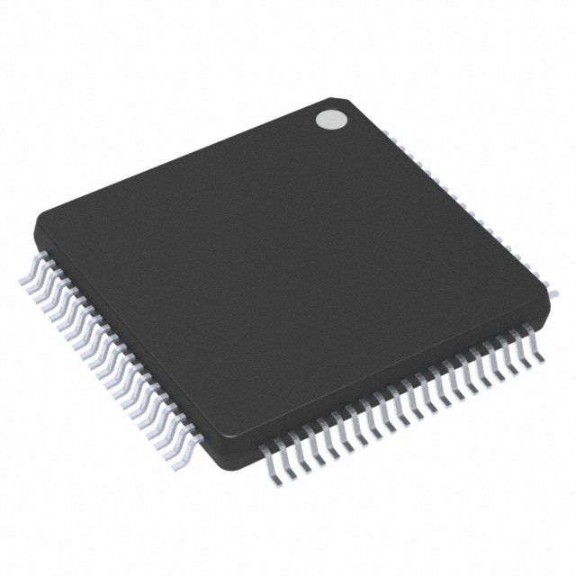
Package Information
Plastic Package
80-Pin LQFP, 12 x 12 mm, 0.5 mm pitch
Ordering Information
See Table 1 on page 4
1
i.MX RT1010 introduction
The i.MX RT1010 is a member of i.MX RT real-time
processor family based on the Arm® Cortex®-M7 core,
which operates at speeds up to 500 MHz to provide high
CPU performance and best real-time response.
The i.MX RT1010 processor has 128 KB on-chip RAM,
which can be flexibly configured as TCM or
general-purpose on-chip RAM. The i.MX RT1010
integrates advanced power management module with
DCDC and LDO that reduces complexity of external
power supply and simplifies power sequencing. The
i.MX RT1010 also provides various memory interfaces,
including Quad SPI, and a wide range of connectivity
interfaces, including UART, SPI, I2C, and USB; for
connecting peripherals including WLAN, Bluetooth™,
and GPS. The i.MX RT1010 also has rich audio features,
including SPDIF and I2S audio interface. Various analog
IP integration, including ADC, temperature sensor, and
etc.
NXP reserves the right to change the production detail specifications as may be required
to permit improvements in the design of its products.
1. i.MX RT1010 introduction . . . . . . . . . . . . . . . . . . . . . . . . 1
1.1. Features . . . . . . . . . . . . . . . . . . . . . . . . . . . . . . . . 2
1.2. Ordering information . . . . . . . . . . . . . . . . . . . . . . . 4
2. Architectural overview . . . . . . . . . . . . . . . . . . . . . . . . . . . 6
2.1. Block diagram . . . . . . . . . . . . . . . . . . . . . . . . . . . . 6
3. Modules list . . . . . . . . . . . . . . . . . . . . . . . . . . . . . . . . . . . 7
3.1. Special signal considerations . . . . . . . . . . . . . . . 12
3.2. Recommended connections for unused analog
interfaces . . . . . . . . . . . . . . . . . . . . . . . . . . . . . . . 13
4. Electrical characteristics . . . . . . . . . . . . . . . . . . . . . . . . 15
4.1. Chip-level conditions . . . . . . . . . . . . . . . . . . . . . . 15
4.2. System power and clocks . . . . . . . . . . . . . . . . . . 21
4.3. I/O parameters . . . . . . . . . . . . . . . . . . . . . . . . . . 27
4.4. System modules . . . . . . . . . . . . . . . . . . . . . . . . . 30
4.5. External memory interface . . . . . . . . . . . . . . . . . 34
4.6. Audio . . . . . . . . . . . . . . . . . . . . . . . . . . . . . . . . . . 40
4.7. Analog . . . . . . . . . . . . . . . . . . . . . . . . . . . . . . . . . 43
4.8. Communication interfaces . . . . . . . . . . . . . . . . . . 49
4.9. Timers . . . . . . . . . . . . . . . . . . . . . . . . . . . . . . . . . 54
5. Boot mode configuration . . . . . . . . . . . . . . . . . . . . . . . . 55
5.1. Boot mode configuration pins . . . . . . . . . . . . . . . 55
5.2. Boot device interface allocation . . . . . . . . . . . . . . 55
6. Package information and contact assignments . . . . . . . 57
6.1. 12 x 12 mm package information . . . . . . . . . . . . 57
7. Revision history . . . . . . . . . . . . . . . . . . . . . . . . . . . . . . . 64
�i.MX RT1010 introduction
The i.MX RT1010 is specifically useful for applications, such as:
• Audio
• Industrial
• Motor Control
• Home Appliance
• IoT
1.1
Features
The i.MX RT1010 processors are based on Arm Cortex-M7 MPCore™ Platform, which has the
following features:
• Supports single Arm® Cortex®-M7 with:
— 16 KB L1 Instruction Cache
— 8 KB L1 Data Cache
— Full featured Floating Point Unit (FPU) with support of the VFPv5 architecture
— Support the Armv7-M Thumb instruction set, defined in the ARM v7-M architecture
• Integrated MPU, up to 16 individual protection regions
• Up to 128 KB I-TCM and D-TCM in total
• Up to 500 MHz frequency
• Cortex® M7 CoreSight™ components integration for debug
• Frequency of the core, as per Table 9, "Operating ranges," on page 16.
The SoC-level memory system consists of the following additional components:
— Boot ROM (64 KB)
— On-chip RAM (128 KB)
– Configurable RAM size up to 128 KB shared with CM7 TCM
• External memory interfaces:
— SPI NOR FLASH
— Single/Dual channel Quad SPI FLASH with XIP support and on-the-fly decryption
— Octal flash
• Timers and PWMs:
— Two General Programmable Timers (GPT)
– 4-channel generic 32-bit resolution timer for each
– Each support standard capture and compare operation
— Periodical Interrupt Timer (PIT)
– Generic 32-bit resolution timer
– Periodical interrupt generation
— FlexPWM
– Up to 4 submodules
i.MX RT1010 Crossover Processors Data Sheet for Consumer Products, Rev. 0, 09/2019
2
NXP Semiconductors
�i.MX RT1010 introduction
– 16-bit resolution PWM suitable for Motor Control applications
Each i.MX RT1010 processor enables the following interfaces to external devices (some of them are
muxed and not available simultaneously):
• Audio:
— SPDIF input and output
— Two synchronous audio interface (SAI) modules, which support I2S, AC97, TDM, and
codec/DSP interfaces
— MQS interface for medium quality audio via GPIO pads
• Connectivity:
— One USB 2.0 OTG controller with integrated PHY interface
— Four universal asynchronous receiver/transmitter (UART) modules
— Two I2C modules
— Two SPI modules
• GPIO and Pin Multiplexing:
— General-purpose input/output (GPIO) modules with interrupt capability
— Input/output multiplexing controller (IOMUXC) to provide centralized pad control
— 44 GPIOs for 80-pin LQFP package
— FlexIO
The i.MX RT1010 processors integrate advanced power management unit and controllers:
• Full PMIC integration, including on-chip DCDC and LDOs
• Temperature sensor with programmable trim points
• GPC hardware power management controller
The i.MX RT1010 processors support the following system debug:
• Arm® Cortex®-M7 CoreSight debug and trace architecture
• Trace Port Interface Unit (TPIU) to support off-chip real-time trace
• Support for 5-pin JTAG and SWD debug interfaces1
Security functions are enabled and accelerated by the following hardware:
• High Assurance Boot (HAB)
• Data Co-Processor (DCP):
— AES-128, ECB, and CBC mode
— SHA-1 and SHA-256
— CRC-32
• FlexSPI with On-The-Fly AES Decryption (OTFAD)
— AES-128, CTR mode
— On-the-fly QSPI Flash decryption
• True random number generation (TRNG)
1. SWD is the default debug interface.
i.MX RT1010 Crossover Processors Data Sheet for Consumer Products, Rev. 0, 09/2019
NXP Semiconductors
3
�i.MX RT1010 introduction
•
•
Secure Non-Volatile Storage (SNVS)
— Secure real-time clock (RTC)
— Zero Master Key (ZMK)
Secure JTAG Controller (SJC)
NOTE
The actual feature set depends on the part numbers as described in Table 1.
Functions such as connectivity interfaces, and security features are not
offered on all derivatives.
1.2
Ordering information
Table 1 provides orderable part numbers covered by this data sheet.
Table 1. Ordering information
Part Number
MIMXRT1011DAE5A
Features
• 500 MHz, consumer
grade for general
purpose
• DMA
• Boot ROM (64KB)
• On-chip RAM
(128KB)
• USB OTG x1
• SAI x2
• SPDIF x1
• MQS x1
• GPT x2
• PWM x1
• 4-channel PIT
• WDOG x4
• UART x4
• I2C x2
•
•
•
•
•
•
•
•
•
•
•
•
•
Junction
Temperature
Tj (C)
Package
SPI x2
12 x 12 mm 80-pin LQFP, 0.5 0 to 95
KPP
mm pitch
ADC x1
FlexSPI
FLEXIO
GPIO
HAB/DCP/OTFAD
TRNG
SNVS
SJC
DCDC
Temperature sensor
GPC hardware power
management
controller
Figure 1 describes the part number nomenclature so that characteristics of a specific part number can be
identified (for example, cores, frequency, temperature grade, fuse options, and silicon revision). The
primary characteristic which describes which data sheet applies to a specific part is the temperature grade
(junction) field.
Ensure to have the proper data sheet for specific part by verifying the temperature grade (junction) field
and matching it to the proper data sheet. If there are any questions, visit the web page nxp.com/IMXRT or
contact an NXP representative for details.
i.MX RT1010 Crossover Processors Data Sheet for Consumer Products, Rev. 0, 09/2019
4
NXP Semiconductors
�i.MX RT1010 introduction
M
IMX
XX
@
##
%
+
VV
$
A
Qualification Level
M
Silicon Rev
A
Prototype Samples
P
A0
A
Mass Production
M
Special
S
Part # series
XX
i.MX RT
RT
Frequency
$
400 MHz
4
500 MHz
5
Family
@
600 MHz
6
First Generation RT family
1
700 MHz
7
Reserved
2
800 MHz
8
1000 MHz
A
3
4
5
6
VV
Package Type
7
AE
80-pin LQFP, 12 x 12 mm, 0.5 mm pitch
8
Sub-Family
##
01
RT1010
02
RT1020
Tie
05
RT1050
1
Standard Feature General Purpose
06
RT1060
5
Enhanced Feature
%
Temperature
+
Consumer: 0 to + 95 °C
D
Industrial: -40 to +105 °C
C
Figure 1. Part number nomenclature—i.MX RT1010
i.MX RT1010 Crossover Processors Data Sheet for Consumer Products, Rev. 0, 09/2019
NXP Semiconductors
5
�Architectural overview
2
Architectural overview
The following subsections provide an architectural overview of the i.MX RT1010 processor system.
2.1
Block diagram
Figure 2 shows the functional modules in the i.MX RT1010 processor system1.
CPU Platform
System Control
Connectivity
ARM Cortex-M7
Security JTAG
16 KB I-cache
UART x4
8 KB D-cache
4 x 4 Keypad
PLL / OSC
RTC and Reset
FPU
NVIC
HSGPIO
MPU
I2C x2
128K I-TCM and D-TCM
SPI x2
Embedded DMA
IOMUX
GP Timer x3
FlexIO
External Memory
Dual-Channel Quad-SPI
GPIO
Octal/Hyper Flash/RAM
FlexPWM x1
I2S / SAI x2
FlexSPI with on-the-fly AES decryption
SPDIF Tx/Rx
Security
Watch Dog x4
MQS
HAB
Power Management
USB2.0 OTG with PHY x1
DCDC
LDO
Ciphers
RNG
Internal Memory
Temp Monitor
128 KB SRAM shared with TCM
ADC
Secure RTC
eFuse
64 KB ROM
ADC (15-ch) x1
.
Figure 2. i.MX RT1010 system block diagram
1. Some modules shown in this block diagram are not offered on all derivatives. See Table 1 for details.
i.MX RT1010 Crossover Processors Data Sheet for Consumer Products, Rev. 0, 09/2019
6
NXP Semiconductors
�Modules list
3
Modules list
The i.MX RT1010 processors contain a variety of digital and analog modules. Table 2 describes these
modules in alphabetical order.
Table 2. i.MX RT1010 modules list
Block mnemonic
Block name
Subsystem
Brief description
ADC1
Analog to Digital
Converter
Analog
The ADC is a 12-bit general purpose analog to digital
converter.
ADC_ETC
ADC External Trigger
Control
Analog
The ADC_ETC enables multiple users to share an ADC
module in a Time-Division-Multiplexing (TDM) way.
AOI
And-Or-Inverter
Cross Trigger
The AOI provides a universal boolean function
generator with using a four team sum of products
expression, for each product term containing true or
complement values of the four selected inputs (A, B, C,
D).
Arm
Arm Platform
Arm
The Arm Core Platform includes 1x Cortex-M7 core. It
also includes associated sub-blocks, such as Nested
Vectored Interrupt Controller (NVIC), Floating-Point
Unit (FPU), Memory Protection Unit (MPU), and
CoreSight debug modules.
CCM
GPC
SRC
Clock Control Module,
Clocks, Resets, and These modules are responsible for clock and reset
General Power
Power Control
distribution in the system, and also for the system
Controller, System Reset
power management.
Controller
CSU
Central Security Unit
Security
The Central Security Unit (CSU) is responsible for
setting comprehensive security policy within the i.MX
RT1010 platform.
DAP
Debug Access Port
System Control
Peripherals
The DAP provides real-time access for the debugger
without halting the core to:
• System memory and peripheral registers
• All debug configuration registers
The DAP also provides debugger access to JTAG scan
chains. The DAP module is internal to the Cortex-M7
Core Platform.
DCDC
DCDC Converter
Analog
The DCDC module is used for generating power supply
for core logic. Main features are:
• Adjustable high efficiency regulator
• Supports 3.3 V input voltage
• Supports nominal run and low power standby modes
• Supports at 0.9 ~ 1.3 V output in run mode
• Supports at 0.9 ~ 1.0 V output in standby mode
• Over current and over voltage detection
i.MX RT1010 Crossover Processors Data Sheet for Consumer Products, Rev. 0, 09/2019
NXP Semiconductors
7
�Modules list
Table 2. i.MX RT1010 modules list (continued)
Block mnemonic
Block name
Subsystem
Brief description
eDMA
enhanced Direct Memory System Control
Access
Peripherals
There is an enhanced DMA (eDMA) engine and
DMA_MUX.
• The eDMA is a 16-channel DMA engine, which is
capable of performing complex data transfers with
minimal intervention from a host processor.
• The DMA_MUX is capable of multiplexing up to 128
DMA request sources to the 16 DMA channels of
eDMA.
EWM
External Watchdog
Monitor
Timer Peripherals
The EWM modules is designed to monitor external
circuits, as well as the software flow. This provides a
back-up mechanism to the internal WDOG that can
reset the system. The EWM differs from the internal
WDOG in that it does not reset the system. The EWM,
if allowed to time-out, provides an independent trigger
pin that when asserted resets or places an external
circuit into a safe mode.
FlexIO1
Flexible Input/output
Connectivity and
Communications
The FlexIO is capable of supporting a wide range of
protocols including, but not limited to: UART, I2C, SPI,
I2S, camera interface, display interface, PWM
waveform generation, etc. The module can remain
functional when the chip is in a low power mode
provided the clock it is using remain active.
FlexPWM1
Pulse Width Modulation
Timer Peripherals
The pulse-width modulator (PWM) contains four PWM
sub-modules, each of which is set up to control a single
half-bridge power stage. Fault channel support is
provided. The PWM module can generate various
switching patterns, including highly sophisticated
waveforms.
FlexRAM
RAM
Memories
The i.MX RT1010 has 128 KB of on-chip RAM which
could be flexible allocated to I-TCM, D-TCM, and
on-chip RAM (OCRAM) in a 32 KB granularity. The
FlexRAM is the manager of the 128 KB on-chip RAM
array. Major functions of this blocks are: interfacing to
I-TCM and D-TCM of Arm core and OCRAM controller;
dynamic RAM arrays allocation for I-TCM, D-TCM, and
OCRAM.
FlexSPI
Quad Serial Peripheral
Interface
Connectivity and
Communications
FlexSPI acts as an interface to one or two external
serial flash devices, each with up to four bidirectional
data lines.
GPIO1
GPIO2
GPIO5
General Purpose I/O
Modules
System Control
Peripherals
Used for general purpose input/output to external ICs.
Each GPIO module supports up to 32 bits of I/O.
i.MX RT1010 Crossover Processors Data Sheet for Consumer Products, Rev. 0, 09/2019
8
NXP Semiconductors
�Modules list
Table 2. i.MX RT1010 modules list (continued)
Block mnemonic
Block name
Subsystem
Brief description
GPT1
GPT2
General Purpose Timer
Timer Peripherals
Each GPT is a 32-bit “free-running” or “set and forget”
mode timer with programmable prescaler and compare
and capture register. A timer counter value can be
captured using an external event and can be configured
to trigger a capture event on either the leading or trailing
edges of an input pulse. When the timer is configured to
operate in “set and forget” mode, it is capable of
providing precise interrupts at regular intervals with
minimal processor intervention. The counter has output
compare logic to provide the status and interrupt at
comparison. This timer can be configured to run either
on an external clock or on an internal clock.
KPP
Keypad Port
Human Machine
Interfaces
The KPP is a 16-bit peripheral that can be used as a
keypad matrix interface or as general purpose
input/output (I/O). It supports 8 x 8 external key pad
matrix. Main features are:
• Multiple-key detection
• Long key-press detection
• Standby key-press detection
• Supports a 2-point and 3-point contact key matrix
LPI2C1
LPI2C2
Low Power
Inter-integrated Circuit
Connectivity and
Communications
The LPI2C is a low power Inter-Integrated Circuit (I2C)
module that supports an efficient interface to an I2C bus
as a master.
The I2C provides a method of communication between
a number of external devices. More detailed
information, see Section 4.8.2, "LPI2C module timing
parameters".
LPSPI1
LPSPI2
Low Power Serial
Peripheral Interface
Connectivity and
Communications
The LPSPI is a low power Serial Peripheral Interface
(SPI) module that support an efficient interface to an
SPI bus as a master and/or a slave.
• It can continue operating while the chip is in stop
mode, if an appropriate clock is available.
• Designed for low CPU overhead, with DMA off
loading of FIFO register access.
LPUART1
LPUART2
LPUART3
LPUART4
UART Interface
Connectivity
Peripherals
Each of the UART modules support the following serial
data transmit/receive protocols and configurations:
• 7- bit or 8-bit data words, 1 or 2 stop bits,
programmable parity (even, odd or none)
• Programmable baud rates up to 5 Mbps.
OTFAD
On-the-Fly AES
Decryption
Security
OTFAD co-works with FlexSPI to provide superior
cryptographic decryption capabilities without
compromising system performance.
PIT
Periodical Interrupt Timer Timer Peripherals
The PIT features 32-bit counter timer, programmable
count modules, clock division, interrupt generation, and
a slave mode to synchronize count enable for multiple
PITs.
MQS
Medium Quality Sound
MQS is used to generate 2-channel medium quality
PWM-like audio via two standard digital GPIO pins.
Multimedia
Peripherals
i.MX RT1010 Crossover Processors Data Sheet for Consumer Products, Rev. 0, 09/2019
NXP Semiconductors
9
�Modules list
Table 2. i.MX RT1010 modules list (continued)
Block mnemonic
Block name
Subsystem
Brief description
ROMCP
ROM Controller with
Patch
Memories and
The ROMCP acts as an interface between the Arm
Memory Controllers advanced high-performance bus and the ROM. The
on-chip ROM is only used by the Cortex-M7 core during
boot up. Size of the ROM is 64 KB.
RTC OSC
Real Time Clock
Oscillator
Clock Sources and
Control
The RTC OSC provides the clock source for the
Real-Time Clock module. The RTC OSC module, in
conjunction with an external crystal, generates a 32.678
kHz reference clock for the RTC.
RTWDOG
Watch Dog
Timer Peripherals
The RTWDG module is a high reliability independent
timer that is available for system to use. It provides a
safety feature to ensure software is executing as
planned and the CPU is not stuck in an infinite loop or
executing unintended code. If the WDOG module is not
serviced (refreshed) within a certain period, it resets the
MCU. Windowed refresh mode is supported as well.
SAI1
SAI3
Synchronous Audio
Interface
Multimedia
Peripherals
The SAI module provides a synchronous audio
interface (SAI) that supports full duplex serial interfaces
with frame synchronization, such as I2S, AC97, TDM,
and codec/DSP interfaces.
SA-TRNG
Standalone True Random Security
Number Generator
The SA-TRNG is hardware accelerator that generates
a 512-bit entropy as needed by an entropy consuming
module or by other post processing functions.
SJC
Secure JTAG Controller
System Control
Peripherals
The SJC provides JTAG interface, which complies with
JTAG TAP standards, to internal logic. The i.MX
RT1010 processors use JTAG port for production,
testing, and system debugging. In addition, the SJC
provides BSR (Boundary Scan Register) standard,
which complies with IEEE1149.1 and IEEE1149.6.
The JTAG port is accessible during platform initial
laboratory bring-up, for manufacturing tests and
troubleshooting, as well as for software debugging by
authorized entities. The i.MX RT1010 SJC incorporates
three security modes for protecting against
unauthorized accesses. Modes are selected through
eFUSE configuration.
SNVS
Secure Non-Volatile
Storage
Security
Secure Non-Volatile Storage, including Secure Real
Time Clock, Security State Machine, and Master Key
Control.
SPDIF
Sony Philips Digital
Interconnect Format
Multimedia
Peripherals
A standard audio file transfer format, developed jointly
by the Sony and Phillips corporations. It has Transmitter
and Receiver functionality.
Temp Monitor
Temperature Monitor
Analog
The temperature sensor implements a temperature
sensor/conversion function based on a
temperature-dependent voltage to time conversion.
i.MX RT1010 Crossover Processors Data Sheet for Consumer Products, Rev. 0, 09/2019
10
NXP Semiconductors
�Modules list
Table 2. i.MX RT1010 modules list (continued)
Block mnemonic
Block name
Subsystem
Brief description
USB 2.0
Universal Serial Bus 2.0
Connectivity
Peripherals
USB 2.0 (USB OTG1) contains:
• One high-speed OTG 2.0 module with integrated HS
USB PHY
• Support eight Transmit (TX) and eight Receive (RX)
endpoints, including endpoint 0
WDOG1
WDOG2
WDOG3
Watch Dog
Timer Peripherals
The Watch Dog Timer supports two comparison points
during each counting period. Each of the comparison
points is configurable to evoke an interrupt to the Arm
core, and a second point evokes an external event on
the WDOG line.
XBAR
Cross BAR
Cross Trigger
Each crossbar switch is an array of muxes with shared
inputs. Each mux output provides one output of the
crossbar. The number of inputs and the number of
muxes/outputs are user configurable and registers are
provided to select which of the shared inputs are routed
to each output.
i.MX RT1010 Crossover Processors Data Sheet for Consumer Products, Rev. 0, 09/2019
NXP Semiconductors
11
�Modules list
3.1
Special signal considerations
Table 3 lists special signal considerations for the i.MX RT1010 processors. The signal names are listed in
alphabetical order.
The package contact assignments can be found in Section 6, "Package information and contact
assignments".” Signal descriptions are provided in the i.MX RT1010 Reference Manual
(IMXRT1010RM).
Table 3. Special signal considerations
Signal name
Remarks
DCDC_PSWITCH
PAD is in DCDC_IN domain and connected the ground to bypass DCDC.
To enable DCDC function, assert to DCDC_IN with at least 1 ms delay for DCDC_IN rising edge.
RTC_XTALI/RTC_XTALO
If the user wishes to configure RTC_XTALI and RTC_XTALO as an RTC oscillator, a 32.768 kHz
crystal, (100 k ESR, 10 pF load) should be connected between RTC_XTALI and RTC_XTALO.
Keep in mind the capacitors implemented on either side of the crystal are about twice the crystal
load capacitor. To hit the exact oscillation frequency, the board capacitors need to be reduced to
account for board and chip parasitics. The integrated oscillation amplifier is self biasing, but
relatively weak. Care must be taken to limit parasitic leakage from RTC_XTALI and RTC_XTALO
to either power or ground (>100 M). This will debias the amplifier and cause a reduction of
startup margin. Typically RTC_XTALI and RTC_XTALO should bias to approximately 0.5 V.
If it is desired to feed an external low frequency clock into RTC_XTALI, the RTC_XTALO pin must
remain unconnected or driven with a complimentary signal. The logic level of this forcing clock
should not exceed VDD_SNVS_CAP level and the frequency should be 500, 500
—
532.04
—
s
1
Typical value is the average value of total test.
The temperature is at 25oC.
3 The code runs in the ITCM.
2
4.5
External memory interface
The following sections provide information about external memory interfaces.
4.5.1
FlexSPI parameters
Measurements are with a load 15 pf and input slew rate of 1 V/ns.
4.5.1.1
FlexSPI input/read timing
There are three sources for the internal sample clock for FlexSPI read data:
• Dummy read strobe generated by FlexSPI controller and looped back internally
(FlexSPIn_MCR0[RXCLKSRC] = 0x0)
• Dummy read strobe generated by FlexSPI controller and looped back through the
DQS pad (FlexSPIn_MCR0[RXCLKSRC] = 0x1)
• Read strobe provided by memory device and input from DQS pad
(FlexSPIn_MCR0[RXCLKSRC] = 0x3)
The following sections describe input signal timing for each of these four internal sample clock sources.
i.MX RT1010 Crossover Processors Data Sheet for Consumer Products, Rev. 0, 09/2019
34
NXP Semiconductors
�Electrical characteristics
4.5.1.1.1
SDR mode with FlexSPIn_MCR0[RXCLKSRC] = 0x0, 0x1
Table 27. FlexSPI input timing in SDR mode where FlexSPIn_MCR0[RXCLKSRC] = 0X0
Symbol
Parameter
Min
Max
Unit
—
60
MHz
—
Frequency of operation
TIS
Setup time for incoming data
8.67
—
ns
TIH
Hold time for incoming data
0
—
ns
Table 28. FlexSPI input timing in SDR mode where FlexSPIn_MCR0[RXCLKSRC] = 0X1
Symbol
Parameter
Min
Max
Unit
—
Frequency of operation
—
133
MHz
TIS
Setup time for incoming data
2
—
ns
TIH
Hold time for incoming data
1
—
ns
SCK
TIS
TIH
TIS
TIH
SIO[0:7]
Internal Sample Clock
Figure 15. FlexSPI input timing in SDR mode where FlexSPIn_MCR0[RXCLKSRC] = 0X0, 0X1
NOTE
Timing shown is based on the memory generating read data on the SCK
falling edge, and FlexSPI controller sampling read data on the falling edge.
4.5.1.1.2
SDR mode with FlexSPIn_MCR0[RXCLKSRC] = 0x3
There are two cases when the memory provides both read data and the read strobe in SDR mode:
• A1–Memory generates both read data and read strobe on SCK rising edge (or falling
edge)
• A2–Memory generates read data on SCK falling edge and generates read strobe on
SCK rising edgeSCK rising edge
i.MX RT1010 Crossover Processors Data Sheet for Consumer Products, Rev. 0, 09/2019
NXP Semiconductors
35
�Electrical characteristics
Table 29. FlexSPI input timing in SDR mode where FlexSPIn_MCR0[RXCLKSRC] = 0x3 (Case A1)
Value
Symbol
Parameter
Unit
Min
Max
—
Frequency of operation
—
133
MHz
TSCKD
Time from SCK to data valid
—
—
ns
TSCKDQS
Time from SCK to DQS
—
—
ns
TSCKD - TSCKDQS
Time delta between TSCKD and TSCKDQS
-2
2
ns
SCK
TSCKD
TSCKD
SIO[0:7]
TSCKDQS
TSCKDQS
DQS
Figure 16. FlexSPI input timing in SDR mode where FlexSPIn_MCR0[RXCLKSRC] = 0X3 (Case A1)
NOTE
Timing shown is based on the memory generating read data and read strobe
on the SCK rising edge. The FlexSPI controller samples read data on the
DQS falling edge.
Table 30. FlexSPI input timing in SDR mode where FlexSPIn_MCR0[RXCLKSRC] = 0x3 (Case A2)
Value
Symbol
Parameter
Unit
Min
Max
—
Frequency of operation
—
133
MHz
TSCKD
Time from SCK to data valid
—
—
ns
TSCKDQS
Time from SCK to DQS
—
—
ns
TSCKD - TSCKDQS
Time delta between TSCKD and TSCKDQS
-2
2
ns
i.MX RT1010 Crossover Processors Data Sheet for Consumer Products, Rev. 0, 09/2019
36
NXP Semiconductors
�Electrical characteristics
SCK
TSCKD
TSCKD
TSCKD
SIO[0:7]
TSCKDQS
TSCKDQS
TSCKDQS
DQS
Internal Sample Clock
Figure 17. FlexSPI input timing in SDR mode where FlexSPIn_MCR0[RXCLKSRC] = 0X3 (Case A2)
NOTE
Timing shown is based on the memory generating read data on the SCK
falling edge and read strobe on the SCK rising edge. The FlexSPI controller
samples read data on a half cycle delayed DQS falling edge.
4.5.1.1.3
DDR mode with FlexSPIn_MCR0[RXCLKSRC] = 0x0, 0x1
Table 31. FlexSPI input timing in DDR mode where FlexSPIn_MCR0[RXCLKSRC] = 0x0
Symbol
Parameter
Min
Max
Unit
—
30
MHz
—
Frequency of operation
TIS
Setup time for incoming data
8.67
—
ns
TIH
Hold time for incoming data
0
—
ns
Table 32. FlexSPI input timing in DDR mode where FlexSPIn_MCR0[RXCLKSRC] = 0x1
Symbol
Parameter
Min
Max
Unit
—
Frequency of operation
—
66
MHz
TIS
Setup time for incoming data
2
—
ns
TIH
Hold time for incoming data
1
—
ns
SCLK
TIS
TIH
TIS
TIH
SIO[0:7]
Internal Sample Clock
Figure 18. FlexSPI input timing in DDR mode where FlexSPIn_MCR0[RXCLKSRC] = 0x0, 0x1
i.MX RT1010 Crossover Processors Data Sheet for Consumer Products, Rev. 0, 09/2019
NXP Semiconductors
37
�Electrical characteristics
4.5.1.1.4
DDR mode with FlexSPIn_MCR0[RXCLKSRC] = 0x3
There are two cases when the memory provides both read data and the read strobe in DDR mode:
• B1–Memory generates both read data and read strobe on SCK edge
• B2–Memory generates read data on SCK edge and generates read strobe on SCK2
edge
Table 33. FlexSPI input timing in DDR mode where FlexSPIn_MCR0[RXCLKSRC] = 0x3 (Case B1)
Symbol
Parameter
Min
Max
Unit
—
Frequency of operation
—
133
MHz
TSCKD
Time from SCK to data valid
—
—
ns
TSCKDQS
Time from SCK to DQS
—
—
ns
TSCKD - TSCKDQS
Time delta between TSCKD and TSCKDQS
-1
1
ns
SCK
TSCKD
SIO[0:7]
TSCKDQS
DQS
Figure 19. FlexSPI input timing in DDR mode where FlexSPIn_MCR0[RXCLKSRC] = 0x3 (Case B1)
Table 34. FlexSPI input timing in DDR mode where FlexSPIn_MCR0[RXCLKSRC] = 0x3 (Case B2)
Symbol
Parameter
Min
Max
Unit
—
Frequency of operation
—
133
MHz
TSCKD
Time from SCK to data valid
—
—
ns
TSCKD - TSCKDQS
Time delta between TSCKD and TSCKDQS
-1
1
ns
i.MX RT1010 Crossover Processors Data Sheet for Consumer Products, Rev. 0, 09/2019
38
NXP Semiconductors
�Electrical characteristics
SCK
TSCKD
SIO[0:7]
SCK2
TSCK2DQS
DQS
Figure 20. FlexSPI input timing in DDR mode where FlexSPIn_MCR0[RXCLKSRC] = 0x3 (Case B2)
4.5.1.2
FlexSPI output/write timing
The following sections describe output signal timing for the FlexSPI controller including control signals
and data outputs.
4.5.1.2.1
SDR mode
Table 35. FlexSPI output timing in SDR mode
Symbol
Parameter
Min
Max
Unit
—
Frequency of operation
—
1331
MHz
Tck
SCK clock period
6.0
—
ns
TDVO
Output data valid time
—
1
ns
TDHO
Output data hold time
-1
—
ns
TCSS
Chip select output setup time
3 x TCK -1
—
ns
TCSH
Chip select output hold time
3 x TCK + 2
—
ns
1
The actual maximum frequency supported is limited by the FlexSPIn_MCR0[RXCLKSRC] configuration used. Please refer to the FlexSPI SDR input timing
specifications.
NOTE
TCSS and TCSH are configured by the FlexSPIn_FLSHAxCR1
register, the default values are shown above. Please refer to the i.MX
RT1010 Reference Manual (IMXRT1010RM) for more details.
SCK
T CSS
TCSH
T CK
CS
TDVO
TDVO
SIO[0:7]
TDHO
TDHO
Figure 21. FlexSPI output timing in SDR mode
i.MX RT1010 Crossover Processors Data Sheet for Consumer Products, Rev. 0, 09/2019
NXP Semiconductors
39
�Electrical characteristics
4.5.1.2.2
DDR mode
Table 36. FlexSPI output timing in DDR mode
Symbol
Parameter
Min
Max
Unit
—
Frequency of operation1
—
133
MHz
Tck
SCK clock period (FlexSPIn_MCR0[RXCLKSRC] = 0x0)
6.0
—
ns
TDVO
Output data valid time
—
2.2
ns
TDHO
Output data hold time
0.8
—
ns
TCSS
Chip select output setup time
3 x TCK / 2 - 0.7
—
ns
TCSH
Chip select output hold time
3 x TCK / 2 + 0.8
—
ns
1
The actual maximum frequency supported is limited by the FlexSPIn_MCR0[RXCLKSRC] configuration used. Please refer to the FlexSPI SDR input timing
specifications.
NOTE
TCSS and TCSH are configured by the FlexSPIn_FLSHAxCR1
register, the default values are shown above. Please refer to the i.MX
RT1010 Reference Manual (IMXRT1010RM) for more details.
SCK
T CSS
T CK
TCSH
CS
TDVO
SIO[0:7]
TDHO
TDVO
TDHO
Figure 22. FlexSPI output timing in DDR mode
4.6
Audio
This section provide information about SAI/I2S and SPDIF.
4.6.1
SAI/I2S switching specifications
This section provides the AC timings for the SAI in master (clocks driven) and slave (clocks input) modes.
All timings are given for non-inverted serial clock polarity (SAI_TCR[TSCKP] = 0, SAI_RCR[RSCKP]
= 0) and non-inverted frame sync (SAI_TCR[TFSI] = 0, SAI_RCR[RFSI] = 0). If the polarity of the clock
and/or the frame sync have been inverted, all the timings remain valid by inverting the clock signal
(SAI_BCLK) and/or the frame sync (SAI_FS) shown in the figures below.
i.MX RT1010 Crossover Processors Data Sheet for Consumer Products, Rev. 0, 09/2019
40
NXP Semiconductors
�Electrical characteristics
Table 37. Master mode SAI timing
Num
Characteristic
Min
Max
Unit
S1
SAI_MCLK cycle time
2 x tsys
—
ns
S2
SAI_MCLK pulse width high/low
40%
60%
MCLK period
S3
SAI_BCLK cycle time
4 x tsys
—
ns
S4
SAI_BCLK pulse width high/low
40%
60%
BCLK period
S5
SAI_BCLK to SAI_FS output valid
—
15
ns
S6
SAI_BCLK to SAI_FS output invalid
0
—
ns
S7
SAI_BCLK to SAI_TXD valid
—
15
ns
S8
SAI_BCLK to SAI_TXD invalid
0
—
ns
S9
SAI_RXD/SAI_FS input setup before SAI_BCLK
15
—
ns
S10
SAI_RXD/SAI_FS input hold after SAI_BCLK
0
—
ns
Figure 23. SAI timing—master modes
Table 38. Slave mode SAI timing
Num
Characteristic
Min
Max
Unit
S11
SAI_BCLK cycle time (input)
4 x tsys
—
ns
S12
SAI_BCLK pulse width high/low (input)
40%
60%
BCLK period
S13
SAI_FS input setup before SAI_BCLK
10
—
ns
S14
SAI_FA input hold after SAI_BCLK
2
—
ns
S15
SAI_BCLK to SAI_TXD/SAI_FS output valid
—
20
ns
S16
SAI_BCLK to SAI_TXD/SAI_FS output invalid
0
—
ns
i.MX RT1010 Crossover Processors Data Sheet for Consumer Products, Rev. 0, 09/2019
NXP Semiconductors
41
�Electrical characteristics
Table 38. Slave mode SAI timing
Num
Characteristic
Min
Max
Unit
S17
SAI_RXD setup before SAI_BCLK
10
—
ns
S18
SAI_RXD hold after SAI_BCLK
2
—
ns
Figure 24. SAI timing—slave modes
4.6.2
SPDIF timing parameters
The Sony/Philips Digital Interconnect Format (SPDIF) data is sent using the bi-phase marking code. When
encoding, the SPDIF data signal is modulated by a clock that is twice the bit rate of the data signal.
Table 39 and Figure 25 and Figure 26 show SPDIF timing parameters for the Sony/Philips Digital
Interconnect Format (SPDIF), including the timing of the modulating Rx clock (SPDIF_SR_CLK) for
SPDIF in Rx mode and the timing of the modulating Tx clock (SPDIF_ST_CLK) for SPDIF in Tx mode.
Table 39. SPDIF timing parameters
Timing parameter range
Characteristics
Symbol
Unit
Min
Max
SPDIF_IN Skew: asynchronous inputs, no specs apply
—
—
0.7
ns
SPDIF_OUT output (Load = 50pf)
• Skew
• Transition rising
• Transition falling
—
—
—
—
—
—
1.5
24.2
31.3
ns
SPDIF_OUT1 output (Load = 30pf)
• Skew
• Transition rising
• Transition falling
—
—
—
—
—
—
1.5
13.6
18.0
Modulating Rx clock (SPDIF_SR_CLK) period
srckp
40.0
—
ns
ns
i.MX RT1010 Crossover Processors Data Sheet for Consumer Products, Rev. 0, 09/2019
42
NXP Semiconductors
�Electrical characteristics
Table 39. SPDIF timing parameters (continued)
Timing parameter range
Characteristics
Symbol
Unit
Min
Max
SPDIF_SR_CLK high period
srckph
16.0
—
ns
SPDIF_SR_CLK low period
srckpl
16.0
—
ns
Modulating Tx clock (SPDIF_ST_CLK) period
stclkp
40.0
—
ns
SPDIF_ST_CLK high period
stclkph
16.0
—
ns
SPDIF_ST_CLK low period
stclkpl
16.0
—
ns
srckp
srckpl
SPDIF_SR_CLK
srckph
VM
VM
(Output)
Figure 25. SPDIF_SR_CLK timing diagram
stclkp
stclkpl
SPDIF_ST_CLK
VM
stclkph
VM
(Input)
Figure 26. SPDIF_ST_CLK timing diagram
4.7
Analog
The following sections provide information about analog interfaces.
4.7.1
DCDC
Table 40 introduces the DCDC electrical specification.
Table 40. DCDC electrical specifications
Mode
Buck mode only, one output
Notes
Input voltage
3.3 V
± 10%
Output voltage
1.1 V
Configurable 0.8 ~ 1.575 with 25 mV one step
Max loading
500 mA
—
Loading in low power modes
200 A ~ 30 mA
—
Efficiency
90% max
@150 mA
i.MX RT1010 Crossover Processors Data Sheet for Consumer Products, Rev. 0, 09/2019
NXP Semiconductors
43
�Electrical characteristics
Table 40. DCDC electrical specifications (continued)
Mode
Buck mode only, one output
Notes
Low power mode
Open loop mode
Ripple is about 15 mV
Run mode
• Always continuous mode
• Support discontinuous mode
Configurable by register
Inductor
4.7 H
—
Capacitor
33 F
—
Over voltage protection
1.6 V
Detect VDDSOC, when the voltage is higher
than 1.6 V, shutdown DCDC.
Over Current protection
1A
Detect the peak current
• Run mode: when the current is larger than
1 A, shutdown DCDC.
• Stop mode: when the current is larger than
250 mA, stop charging the inductor.
Low battery detection
2.6 V
Detect the battery, when battery is lower than
2.6 V, shutdown DCDC.
4.7.2
A/D converter
This section introduces information about A/D converter.
4.7.2.1
12-bit ADC electrical characteristics
The section provide information about 12-bit ADC electrical characteristics.
4.7.2.1.1
12-bit ADC operating conditions
Table 41. 12-bit ADC operating conditions
Characteristic
Conditions
Symb
Typ1
Min
Max
Unit
Comment
Absolute
VDDA
3.0
-
3.6
V
—
Delta to VDD
(VDD-VDDA)2
VDDA
-100
0
100
mV
—
Ground voltage
Delta to VSS
(VSS-VSSAD)
VSSAD
-100
0
100
mV
—
Ref Voltage High
—
VDDA
1.13
VDDA
VDDA
V
—
Ref Voltage Low
—
VSS
VSS
VSS
VSS
V
—
Input Voltage
—
VADIN
VSS
—
VDDA
V
—
Input Capacitance
8/10/12 bit modes
CADIN
—
1.5
2
pF
—
Input Resistance
ADLPC=0, ADHSC=1
RADIN
—
5
7
kohms
—
ADLPC=0, ADHSC=0
—
12.5
15
kohms
—
ADLPC=1, ADHSC=0
—
25
30
kohms
—
Supply voltage
i.MX RT1010 Crossover Processors Data Sheet for Consumer Products, Rev. 0, 09/2019
44
NXP Semiconductors
�Electrical characteristics
Table 41. 12-bit ADC operating conditions (continued)
Characteristic
Analog Source
Resistance
Conditions
12 bit mode fADCK =
40MHz ADLSMP=0,
ADSTS=10, ADHSC=1
Symb
RAS
Typ1
Min
—
—
Max
1
Unit
kohms
Comment
Tsamp=150
ns
RAS depends on Sample Time Setting (ADLSMP, ADSTS) and ADC Power Mode (ADHSC, ADLPC). See charts for Minimum
Sample Time vs RAS
ADC Conversion Clock ADLPC=0, ADHSC=1
Frequency
12 bit mode
fADCK
4
—
40
MHz
—
ADLPC=0, ADHSC=0
12 bit mode
4
—
30
MHz
—
ADLPC=1, ADHSC=0
12 bit mode
4
—
20
MHz
—
1
Typical values assume VDDAD = 3.0 V, Temp = 25°C, fADCK=20 MHz unless otherwise stated. Typical values are for reference
only and are not tested in production.
2 DC potential differences
Figure 27. 12-bit ADC input impedance equivalency diagram
i.MX RT1010 Crossover Processors Data Sheet for Consumer Products, Rev. 0, 09/2019
NXP Semiconductors
45
�Electrical characteristics
12-bit ADC characteristics
Table 42. 12-bit ADC characteristics (VREFH = VDDA, VREFL = VSSAD)
Characteristic
Supply Current
Conditions1
ADLPC=1,
ADHSC=0
Symb
IDDA
Typ2
Min
—
250
ADLPC=0,
ADHSC=0
350
ADLPC=0,
ADHSC=1
400
Max
Unit
Comment
—
µA
ADLSMP = 0, ADSTS
= 10, ADCO = 1
Supply Current
Stop, Reset, Module
Off
IDDA
—
0.01
0.8
µA
—
ADC Asynchronous
Clock Source
ADHSC=0
fADACK
—
10
—
MHz
tADACK = 1/fADACK
—
20
—
—
2
—
cycles
—
Sample Cycles
ADHSC=1
ADLSMP=0,
ADSTS=00
Csamp
ADLSMP=0,
ADSTS=01
4
ADLSMP=0,
ADSTS=10
6
ADLSMP=0,
ADSTS=11
8
ADLSMP=1,
ADSTS=00
12
ADLSMP=1,
ADSTS=01
16
ADLSMP=1,
ADSTS=10
20
ADLSMP=1,
ADSTS=11
24
i.MX RT1010 Crossover Processors Data Sheet for Consumer Products, Rev. 0, 09/2019
46
NXP Semiconductors
�Electrical characteristics
Table 42. 12-bit ADC characteristics (VREFH = VDDA, VREFL = VSSAD) (continued)
Characteristic
Conversion Cycles
Conversion Time
Total Unadjusted
Error
Differential
Non-Linearity
Conditions1
ADLSMP=0
ADSTS=00
Symb
Cconv
Typ2
Min
—
28
ADLSMP=0
ADSTS=01
30
ADLSMP=0
ADSTS=10
32
ADLSMP=0
ADSTS=11
34
ADLSMP=1
ADSTS=00
38
ADLSMP=1
ADSTS=01
42
ADLSMP=1
ADSTS=10
46
ADLSMP=1,
ADSTS=11
50
ADLSMP=0
ADSTS=00
Tconv
—
0.7
ADLSMP=0
ADSTS=01
0.75
ADLSMP=0
ADSTS=10
0.8
ADLSMP=0
ADSTS=11
0.85
ADLSMP=1
ADSTS=00
0.95
ADLSMP=1
ADSTS=01
1.05
ADLSMP=1
ADSTS=10
1.15
ADLSMP=1,
ADSTS=11
1.25
12 bit mode
Comment
cycles
—
—
µs
Fadc = 40 MHz
LSB
1 LSB =
(VREFH VREFL)/2
N
AVGE = 1, AVGS = 11
LSB
AVGE = 1, AVGS = 11
3.4
—
10 bit mode
—
1.5
—
8 bit mode
—
1.2
—
—
0.76
—
10bit mode
—
0.36
—
8 bit mode
—
0.14
—
DNL
Unit
—
—
12 bit mode
TUE
Max
i.MX RT1010 Crossover Processors Data Sheet for Consumer Products, Rev. 0, 09/2019
NXP Semiconductors
47
�Electrical characteristics
Table 42. 12-bit ADC characteristics (VREFH = VDDA, VREFL = VSSAD) (continued)
Characteristic
Conditions1
Integral Non-Linearity 12 bit mode
Zero-Scale Error
Typ2
Max
2.78
—
10bit mode
—
0.61
—
8 bit mode
—
0.14
—
—
-1.14
—
10bit mode
—
-0.25
—
8 bit mode
—
-0.19
—
—
-1.06
—
10bit mode
—
-0.03
—
8 bit mode
—
-0.02
—
10.7
—
12 bit mode
INL
Min
—
12 bit mode
Full-Scale Error
Symb
EZS
EFS
Effective Number of
Bits
12 bit mode
ENOB
10.1
Signal to Noise plus
Distortion
See ENOB
SINAD
SINAD = 6.02 x ENOB + 1.76
1
2
Unit
Comment
LSB
AVGE = 1, AVGS = 11
LSB
AVGE = 1, AVGS = 11
LSB
AVGE = 1, AVGS = 11
Bits
AVGE = 1, AVGS = 11
dB
AVGE = 1, AVGS = 11
All accuracy numbers assume the ADC is calibrated with VREFH=VDDAD
Typical values assume VDDAD = 3.0 V, Temp = 25°C, Fadck=20 MHz unless otherwise stated. Typical values are for reference
only and are not tested in production.
NOTE
The ADC electrical spec is met with the calibration enabled configuration.
Figure 28. Minimum Sample Time Vs Ras (Cas = 2 pF)
i.MX RT1010 Crossover Processors Data Sheet for Consumer Products, Rev. 0, 09/2019
48
NXP Semiconductors
�Electrical characteristics
Figure 29. Minimum Sample Time Vs Ras (Cas = 5 pF)
Figure 30. Minimum Sample Time Vs Ras (Cas = 10 pF)
4.8
Communication interfaces
The following sections provide the information about communication interfaces.
4.8.1
LPSPI timing parameters
The Low Power Serial Peripheral Interface (LPSPI) provides a synchronous serial bus with master and
slave operations. Many of the transfer attributes are programmable. The following tables provide timing
characteristics for classic LPSPI timing modes.
All timing is shown with respect to 20% VDD and 80% VDD thresholds, unless noted, as well as input
signal transitions of 3 ns and a 30 pF maximum load on all LPSPI pins.
i.MX RT1010 Crossover Processors Data Sheet for Consumer Products, Rev. 0, 09/2019
NXP Semiconductors
49
�Electrical characteristics
Table 43. LPSPI Master mode timing
Number
Symbol
Description
Min.
Max.
Units
Note
1
fSCK
Frequency of operation
—
fperiph / 2
MHz
1
2
tSCK
SCK period
2 x tperiph
—
µs
2
3
tLead
Enable lead time
1
—
tperiph
—
4
tLag
Enable lag time
1
—
tperiph
—
5
tWSCK
tSCK / 2 - 3
—
ns
—
6
tSU
Data setup time (inputs)
10
—
ns
—
7
tHI
Data hold time (inputs)
2
—
ns
—
8
tV
Data valid (after SCK edge)
—
8
ns
—
9
tHO
Data hold time (outputs)
0
—
ns
—
Clock (SCK) high or low time
1
Absolute maximum frequency of operation (fop) is 30 MHz. The clock driver in the LPSPI module for fperiph must be
guaranteed this limit is not exceeded.
2 t
periph = 1000 / fperiph
1
PCS
(OUTPUT)
3
2
SCK
(CPOL=0)
(OUTPUT)
4
5
5
SCK
(CPOL=1)
(OUTPUT)
6
SIN
(INPUT)
7
2
MSB IN
BIT 6 . . . 1
LSB IN
8
SOUT
(OUTPUT)
2
MSB OUT
BIT 6 . . . 1
9
LSB OUT
1. If configured as an output.
2. LSBF = 0. For LSBF = 1, bit order is LSB, bit 1, ..., bit 6, MSB.
Figure 31. LPSPI Master mode timing (CPHA = 0)
i.MX RT1010 Crossover Processors Data Sheet for Consumer Products, Rev. 0, 09/2019
50
NXP Semiconductors
�Electrical characteristics
1
PCS
(OUTPUT)
2
4
3
SCK
(CPOL=0)
(OUTPUT)
5
SCK
(CPOL=1)
(OUTPUT)
5
6
SIN
(INPUT)
7
2
MSB IN
BIT 6 . . . 1
9
8
SOUT
(OUTPUT)
LSB IN
2
PORT DATA MASTER MSB OUT
BIT 6 . . . 1
MASTER LSB OUT
PORT DATA
1.If configured as output
2. LSBF = 0. For LSBF = 1, bit order is LSB, bit 1, ..., bit 6, MSB.
Figure 32. LPSPI Master mode timing (CPHA = 1)
s
Table 44. LPSPI Slave mode timing
Number
Symbol
Description
Min.
Max.
Units
Note
1
fSCK
Frequency of operation
0
fperiph / 2
MHz
1
2
tSCK
SCK period
2 x tperiph
—
µs
2
3
tLead
Enable lead time
1
—
tperiph
—
4
tLag
Enable lag time
1
—
tperiph
—
5
tWSCK
tSCK / 2 - 5
—
ns
—
6
tSU
Data setup time (inputs)
2.7
—
ns
—
7
tHI
Data hold time (inputs)
3.8
—
ns
—
8
ta
Slave access time
—
tperiph
ns
3
9
tdis
Slave MISO disable time
—
tperiph
ns
4
10
tV
Data valid (after SCK edge)
—
14.5
ns
—
11
tHO
Data hold time (outputs)
0
—
ns
—
Clock (SCK) high or low time
1
Absolute maximum frequency of operation (fop) is 30 MHz. The clock driver in the LPSPI module for fperiph must be
guaranteed this limit is not exceeded.
2
tperiph = 1000 / fperiph
3 Time to data active from high-impedance state
4 Hold time to high-impedance state
i.MX RT1010 Crossover Processors Data Sheet for Consumer Products, Rev. 0, 09/2019
NXP Semiconductors
51
�Electrical characteristics
PCS
(INPUT)
2
4
SCK
(CPOL=0)
(INPUT)
5
3
SCK
(CPOL=1)
(INPUT)
5
9
8
SIN
(OUTPUT)
see
note
SLAVE MSB
6
SOUT
(INPUT)
10
11
11
BIT 6 . . . 1
SLAVE LSB OUT
SEE
NOTE
7
MSB IN
BIT 6 . . . 1
LSB IN
NOTE: Not defined
Figure 33. LPSPI Slave mode timing (CPHA = 0)
PCS
(INPUT)
4
2
3
SCK
(CPOL=0)
(INPUT)
5
5
SCK
(CPOL=1)
(INPUT)
11
10
SIN
(OUTPUT)
see
note
SLAVE
8
6
SOUT
(INPUT)
MSB OUT
9
BIT 6 . . . 1
SLAVE LSB OUT
BIT 6 . . . 1
LSB IN
7
MSB IN
NOTE: Not defined
Figure 34. LPSPI Slave mode timing (CPHA = 1)
i.MX RT1010 Crossover Processors Data Sheet for Consumer Products, Rev. 0, 09/2019
52
NXP Semiconductors
�Electrical characteristics
4.8.2
LPI2C module timing parameters
This section describes the timing parameters of the LPI2C module.
Table 45. LPI2C module timing parameters
Symbol
fSCL
1
2
Description
SCL clock frequency
Min
Max
Standard mode (Sm)
0
100
Fast mode (Fm)
0
400
Fast mode Plus (Fm+)
0
1000
Ultra Fast mode (UFm)
0
5000
High speed mode (Hs-mode)
0
3400
Unit
kHz
Notes
1, 2
Hs-mode is only supported in slave mode.
See General switching specifications.
4.8.3
LPUART electrical specifications
Please refer to Section 4.3.2.1, "General purpose I/O AC parameters".
4.8.4
USB PHY parameters
This section describes the USB-OTG PHY parameters.
The USB PHY meets the electrical compliance requirements defined in the Universal Serial Bus Revision
2.0 OTG with the following amendments.
• USB ENGINEERING CHANGE NOTICE
— Title: 5V Short Circuit Withstand Requirement Change
— Applies to: Universal Serial Bus Specification, Revision 2.0
• Errata for USB Revision 2.0 April 27, 2000 as of 12/7/2000
• USB ENGINEERING CHANGE NOTICE
— Title: Pull-up/Pull-down resistors
— Applies to: Universal Serial Bus Specification, Revision 2.0
• USB ENGINEERING CHANGE NOTICE
— Title: Suspend Current Limit Changes
— Applies to: Universal Serial Bus Specification, Revision 2.0
• USB ENGINEERING CHANGE NOTICE
— Title: USB 2.0 Phase Locked SOFs
— Applies to: Universal Serial Bus Specification, Revision 2.0
• On-The-Go and Embedded Host Supplement to the USB Revision 2.0 Specification
— Revision 2.0 plus errata and ecn June 4, 2010
• Battery Charging Specification (available from USB-IF)
i.MX RT1010 Crossover Processors Data Sheet for Consumer Products, Rev. 0, 09/2019
NXP Semiconductors
53
�Electrical characteristics
— Revision 1.2, December 7, 2010
— Portable device only
4.9
Timers
This section provide information on timers.
4.9.1
Pulse Width Modulator (PWM) characteristics
This section describes the electrical information of the PWM.
Table 46. PWM timing parameters
Parameter
Symbo
Min
Typ
Max
Unit
PWM Clock Frequency
—
—
—
132
MHz
Power-up Time
tpu
—
25
—
s
i.MX RT1010 Crossover Processors Data Sheet for Consumer Products, Rev. 0, 09/2019
54
NXP Semiconductors
�Boot mode configuration
5
Boot mode configuration
This section provides information on boot mode configuration pins allocation and boot devices interfaces
allocation.
5.1
Boot mode configuration pins
Table 47 provides boot options, functionality, fuse values, and associated pins. Several input pins are also
sampled at reset and can be used to override fuse values, depending on the value of BT_FUSE_SEL fuse.
The boot option pins are in effect when BT_FUSE_SEL fuse is ‘0’ (cleared, which is the case for an
unblown fuse). For detailed boot mode options configured by the boot mode pins, see the i.MX RT1010
Fuse Map document and the System Boot chapter in i.MX RT1010 Reference Manual (IMXRT1010RM).
Table 47. Fuses and associated pins used for boot
Pad
Default setting on reset
eFuse name
GPIO_SD_04
100 K pull-down
src.BOOT_MODE[0]
GPIO_SD_03
100 K pull-down
src.BOOT_MODE[1]
GPIO_SD_02
100 K pull-down
src.BT_CFG[0]
GPIO_SD_01
100 K pull-down
src.BT_CFG[1]
GPIO_SD_00
100 K pull-down
src.BT_CFG[2]
5.2
Details
Boot Options, Pin value overrides fuse
settings for BT_FUSE_SEL = ‘0’.
Signal Configuration as Fuse Override
Input at Power Up.
These are special I/O lines that control
the boot up configuration during
product development. In production,
the boot configuration can be
controlled by fuses.
Boot device interface allocation
The following tables list the interfaces that can be used by the boot process in accordance with the specific
boot mode configuration. The tables also describe the interface’s specific modes and IOMUXC allocation,
which are configured during boot when appropriate.
Table 48. Boot through FlexSPI
PAD Name
IO Function
Mux Mode
Comments
GPIO_SD_04
flexspi.B_DATA[3]
ALT 0
—
GPIO_SD_02
flexspi.B_DATA[2]
ALT 0
—
GPIO_SD_01
flexspi.B_DATA[1]
ALT 0
—
GPIO_SD_03
flexspi.B_DATA[0]
ALT 0
—
GPIO_SD_13
flexspi.B_SCLK
ALT 0
—
GPIO_00
flexspi.B_DQS
ALT 0
—
GPIO_SD_00
flexspi.B_SS0_B
ALT 0
—
GPIO_SD_12
flexspi.A_DQS
ALT 0
—
GPIO_SD_06
flexspi.A_SS0_B
ALT 0
—
i.MX RT1010 Crossover Processors Data Sheet for Consumer Products, Rev. 0, 09/2019
NXP Semiconductors
55
�Boot mode configuration
Table 48. Boot through FlexSPI (continued)
PAD Name
IO Function
Mux Mode
Comments
GPIO_SD_05
flexspi.A_SS1_B
ALT 0
—
GPIO_SD_10
flexspi.A_SCLK
ALT 0
—
GPIO_SD_09
flexspi.A_DATA[0]
ALT 0
—
GPIO_SD_07
flexspi.A_DATA[1]
ALT 0
—
GPIO_SD_08
flexspi.A_DATA[2]
ALT 0
—
GPIO_SD_11
flexspi.A_DATA[3]
ALT 0
—
Table 49. FlexSPI reset
PAD Name
GPIO_13
IO Function
gpiomux.IO[13]
Mux Mode
ALT 5
Comments
—
Table 50. Boot through UART1
PAD Name
IO Function
Mux Mode
Comments
GPIO_10
lpuart1.TX
ALT 0
—
GPIO_09
lpuart1.RX
ALT 0
—
GPIO_08
lpuart1.CTS_B
ALT 6
—
GPIO_07
lpuart1.RTS_B
ALT 6
—
i.MX RT1010 Crossover Processors Data Sheet for Consumer Products, Rev. 0, 09/2019
56
NXP Semiconductors
�Package information and contact assignments
6
Package information and contact assignments
This section includes the contact assignment information and mechanical package drawing.
6.1
6.1.1
12 x 12 mm package information
12 x 12 mm, 0.5 mm pitch, ball matrix
Figure 35 shows the top, bottom, and side views of the 12 x 12 mm LQFP package.
i.MX RT1010 Crossover Processors Data Sheet for Consumer Products, Rev. 0, 09/2019
NXP Semiconductors
57
�Package information and contact assignments
Figure 35. 12 x 12 mm LQFP, case x package top and side views
i.MX RT1010 Crossover Processors Data Sheet for Consumer Products, Rev. 0, 09/2019
58
NXP Semiconductors
�Package information and contact assignments
6.1.2
12 x 12 mm supplies contact assignments and functional contact
assignments
Table 51 shows the device connection list for ground, sense, and reference contact signals.
Table 51. 12 x 12 mm supplies contact Assignment
Supply Rail Name
Pin(s) Position(s)
Remark
DCDC_IN
18
—
DCDC_IN_Q
17
—
DCDC_GND
20
—
DCDC_LP
19
—
DCDC_PSWITCH
15
—
NGND_KEL0
34
—
NVCC_GPIO
7, 50, 63, 71
—
NVCC_PLL
40
—
VDDA_ADC_3P3
42
—
VDD_HIGH_CAP
35
—
VDD_HIGH_IN
39
—
VDD_SNVS_CAP
26
—
VDD_SNVS_IN
25
—
VDD_SOC_IN
14, 53, 77
—
VDD_USB_CAP
31
—
VSS
16, 54, 30, 78
—
VSSA_ADC_3P3
41
Table 52 shows an alpha-sorted list of functional contact assignments for the 12 x 12 mm package.
Table 52. 12 x 12 mm functional contact assignments
Default setting
on Reset
Default Setting
Pin Name
12 x 12
Pin
Power
Group
Pin
Type
Default
Mode
Default
Function
Input/
Output
Value
Input/
Output
Value
GPIO_00
13
NVCC_GPIO
Digital
GPIO
Alt 5
GPIOMUX_IO00
Input
Keeper
Input
100K PD
GPIO_01
12
NVCC_GPIO
Digital
GPIO
Alt 5
GPIOMUX_IO01
Input
Keeper
Input
Keeper
GPIO_02
11
NVCC_GPIO
Digital
GPIO
Alt 5
GPIOMUX_IO02
Input
Keeper
Input
Keeper
GPIO_03
10
NVCC_GPIO
Digital
GPIO
Alt 5
GPIOMUX_IO03
Input
Keeper
Input
Keeper
i.MX RT1010 Crossover Processors Data Sheet for Consumer Products, Rev. 0, 09/2019
NXP Semiconductors
59
�Package information and contact assignments
Table 52. 12 x 12 mm functional contact assignments (continued)
GPIO_04
9
NVCC_GPIO
Digital
GPIO
Alt 5
GPIOMUX_IO04
Input
Keeper
Input
Keeper
GPIO_05
8
NVCC_GPIO
Digital
GPIO
Alt 5
GPIOMUX_IO05
Input
Keeper
Input
Keeper
GPIO_06
6
NVCC_GPIO
Digital
GPIO
Alt 5
GPIOMUX_IO06
Input
Keeper
Input
Keeper
GPIO_07
5
NVCC_GPIO
Digital
GPIO
Alt 5
GPIOMUX_IO07
Input
Keeper
Input
Keeper
GPIO_08
4
NVCC_GPIO
Digital
GPIO
Alt 5
GPIOMUX_IO08
Input
Keeper
Input
Keeper
GPIO_09
3
NVCC_GPIO
Digital
GPIO
Alt 5
GPIOMUX_IO09
Input
Keeper
Input
Keeper
GPIO_10
2
NVCC_GPIO
Digital
GPIO
Alt 5
GPIOMUX_IO10
Input
Keeper
Input
Keeper
GPIO_11
1
NVCC_GPIO
Digital
GPIO
Alt 5
GPIOMUX_IO11
Input
Keeper
Input
Keeper
GPIO_12
80
NVCC_GPIO
Digital
GPIO
Alt 5
GPIOMUX_IO12
Input
Keeper
Input
Keeper
GPIO_13
79
NVCC_GPIO
Digital
GPIO
Alt 5
GPIOMUX_IO13
Input
Keeper
Input
Keeper
GPIO_AD_00
60
NVCC_GPIO
Digital
GPIO
Alt 5
GPIOMUX_IO14
Input
Keeper
Input
Keeper
GPIO_AD_01
59
NVCC_GPIO
Digital
GPIO
Alt 5
GPIOMUX_IO15
Input
Keeper
Input
Keeper
GPIO_AD_02
58
NVCC_GPIO
Digital
GPIO
Alt 5
GPIOMUX_IO16
Input
Keeper
Input
Keeper
GPIO_AD_03
57
NVCC_GPIO
Digital
GPIO
Alt 5
GPIOMUX_IO17
Input
Keeper
Input
Keeper
GPIO_AD_04
56
NVCC_GPIO
Digital
GPIO
Alt 5
GPIOMUX_IO18
Input
Keeper
Output1 Keeper
GPIO_AD_05
55
NVCC_GPIO
Digital
GPIO
Alt 5
GPIOMUX_IO19
Input
Keeper
Input
Keeper
GPIO_AD_06
52
NVCC_GPIO
Digital
GPIO
Alt 5
GPIOMUX_IO20
Input
Keeper
Input
Keeper
GPIO_AD_07
51
NVCC_GPIO
Digital
GPIO
Alt 5
GPIOMUX_IO21
Input
Keeper
Input
Keeper
GPIO_AD_08
49
NVCC_GPIO
Digital
GPIO
Alt 7
JTAG_TRSTB
Input
47K PU
Input
47K PU
GPIO_AD_09
48
NVCC_GPIO
Digital
GPIO
Alt 7
JTAG_TDO
Input
Keeper
Input
Keeper
GPIO_AD_10
47
NVCC_GPIO
Digital
GPIO
Alt 7
JTAG_TDI
Input
47K PU
Input
47K PU
i.MX RT1010 Crossover Processors Data Sheet for Consumer Products, Rev. 0, 09/2019
60
NXP Semiconductors
�Package information and contact assignments
Table 52. 12 x 12 mm functional contact assignments (continued)
GPIO_AD_11
46
NVCC_GPIO
Digital
GPIO
Alt 7
JTAG_MOD
Input
100K PD Input
100K PD
GPIO_AD_12
45
NVCC_GPIO
Digital
GPIO
Alt 7
JTAG_TCK
Input
100K PD Input
100K PD
GPIO_AD_13
44
NVCC_GPIO
Digital
GPIO
Alt 7
JTAG_TMS
Input
47K PU
Input
47K PU
GPIO_AD_14
43
NVCC_GPIO
Digital
GPIO
Alt 5
GPIOMUX_IO28
Input
Keeper
Input
Keeper
GPIO_SD_00
76
NVCC_GPIO
Digital
GPIO
Alt 5
GPIO2_IO00
Input
Keeper
Input
100K PD
GPIO_SD_01
75
NVCC_GPIO
Digital
GPIO
Alt 5
GPIO2_IO01
Input
Keeper
Input
100K PD
GPIO_SD_02
74
NVCC_GPIO
Digital
GPIO
Alt 5
GPIO2_IO02
Input
Keeper
Input
100K PD
GPIO_SD_03
73
NVCC_GPIO
Digital
GPIO
Alt 6
SRC_BOOT_MOD Input
E1
100K PD Input
100K PD
GPIO_SD_04
72
NVCC_GPIO
Digital
GPIO
Alt 6
SRC_BOOT_MOD Input
E0
100K PD Input
100K PD
GPIO_SD_05
70
NVCC_GPIO
Digital
GPIO
Alt 5
GPIO2_IO05
Input
Keeper
Input
Keeper
GPIO_SD_06
69
NVCC_GPIO
Digital
GPIO
Alt 5
GPIO2_IO06
Input
Keeper
Input
Keeper
GPIO_SD_07
68
NVCC_GPIO
Digital
GPIO
Alt 5
GPIO2_IO07
Input
Keeper
Input
Keeper
GPIO_SD_08
67
NVCC_GPIO
Digital
GPIO
Alt 5
GPIO2_IO08
Input
Keeper
Input
Keeper
GPIO_SD_09
66
NVCC_GPIO
Digital
GPIO
Alt 5
GPIO2_IO09
Input
Keeper
Input
Keeper
GPIO_SD_10
65
NVCC_GPIO
Digital
GPIO
Alt 5
GPIO2_IO10
Input
Keeper
Input
Keeper
GPIO_SD_11
64
NVCC_GPIO
Digital
GPIO
Alt 5
GPIO2_IO11
Input
Keeper
Input
Keeper
GPIO_SD_12
62
NVCC_GPIO
Digital
GPIO
Alt 5
GPIO2_IO12
Input
Keeper
Input
Keeper
GPIO_SD_13
61
NVCC_GPIO
Digital
GPIO
Alt 5
GPIO2_IO13
Input
Keeper
Input
100K PD
ONOFF
21
VDD_SNVS_I Digital
N
GPIO
Alt 0
SRC_RESET_B
Input
100K PU Input
100K PU
PMIC_ON_REQ
24
VDD_SNVS_I Digital
N
GPIO
Alt 0
SNVS_PMIC_ON_ Output
REQ
100K PU Output
100K PU
POR_B
22
VDD_SNVS_I Digital
N
GPIO
Alt 0
SRC_POR_B
100K PU Input
100K PU
Input
i.MX RT1010 Crossover Processors Data Sheet for Consumer Products, Rev. 0, 09/2019
NXP Semiconductors
61
�Package information and contact assignments
Table 52. 12 x 12 mm functional contact assignments (continued)
RTC_XTALI
27
—
—
—
—
—
—
—
—
RTC_XTALO
28
—
—
—
—
—
—
—
—
TEST_MODE
23
VDD_SNVS_I Digital
N
GPIO
Alt 0
TCU_TEST_MOD
E
Input
100K PD Input
100K PD
USB_OTG1_CH
D_B
36
—
—
—
—
—
—
—
—
USB_OTG1_DN
32
—
—
—
—
—
—
—
—
USB_OTG1_DP
33
—
—
—
—
—
—
—
—
USB_OTG1_VB
US
29
—
—
—
—
—
—
—
—
XTALI
37
—
—
—
—
—
—
—
—
XTALO
38
—
—
—
—
—
—
—
—
1
This pin output is in a high level until the system reset is complete.
i.MX RT1010 Crossover Processors Data Sheet for Consumer Products, Rev. 0, 09/2019
62
NXP Semiconductors
�Package information and contact assignments
6.1.3
12 x 12 mm package pin assignments
GPIO_SD_10
GPIO_SD_11
NVCC_GPIO
GPIO_SD_12
GPIO_SD_13
63
62
61
GPIO_SD_05
70
64
NVCC_GPIO
71
GPIO_SD_09
GPIO_SD_04
72
65
GPIO_SD_03
73
66
GPIO_SD_02
74
GPIO_SD_08
GPIO_SD_01
75
67
GPIO_SD_00
76
GPIO_SD_06
VDD_SOC_IN
77
GPIO_SD_07
VSS
78
69
GPIO_13
79
68
GPIO_12
80
Figure 36 shows the pin assignments of the 12 x 12 mm package.
1
60
GPIO_AD_00
GPIO_10
2
59
GPIO_AD_01
GPIO_09
3
58
GPIO_AD_02
GPIO_08
4
57
GPIO_AD_03
GPIO_07
5
56
GPIO_AD_04
GPIO_06
6
55
GPIO_AD_05
NVCC_GPIO
7
54
VSS
GPIO_05
8
53
VDD_SOC_IN
GPIO_04
9
52
GPIO_AD_06
GPIO_03
10
51
GPIO_AD_07
GPIO_02
11
50
NVCC_GPIO
GPIO_11
GPIO_01
12
49
GPIO_AD_08
GPIO_00
13
48
GPIO_AD_09
VDD_SOC_IN / DCDC_SENSE
14
47
GPIO_AD_10
DCDC_PSWITCH
15
46
GPIO_AD_11
VSS
16
45
GPIO_AD_12
DCDC_IN_Q
17
44
GPIO_AD_13
35
36
37
38
39
40
VDD_HIGH_CAP
USB_OTG1_CHD_B
XTALI
XTALO
VDD_HIGH_IN
NVCC_PLL
VDD_USB_CAP
34
31
VSS
NGND_KEL0
30
USB_OTG1_VBUS
32
29
33
28
RTC_XTALO
USB_OTG1_DP
27
RTC_XTALI
USB_OTG1_DN
26
VDD_SNVS_IN
ONOFF
VDD_SNVS_CAP
VSSA_ADC_3P3 / ADC_VREFL
25
41
24
20
PMIC_ON_REQ
DCDC_GND
23
VDDA_ADC_3P3 / ADC_VREFH
TEST_MODE
GPIO_AD_14
42
21
43
19
22
18
POR_B
DCDC_IN
DCDC_LP
Figure 36. The pin assignments of the 12 x 12 mm package
i.MX RT1010 Crossover Processors Data Sheet for Consumer Products, Rev. 0, 09/2019
NXP Semiconductors
63
�Revision history
7
Revision history
Table 53 provides a revision history for this data sheet.
Table 53. i.MX RT1010 data sheet document revision history
Rev.
Number
Date
Rev. 0
09/2019
Substantive Change(s)
• Initial version
i.MX RT1010 Crossover Processors Data Sheet for Consumer Products, Rev. 0, 09/2019
64
NXP Semiconductors
�How to Reach Us:
Information in this document is provided solely to enable system and software implementers to
Home Page:
nxp.com
use NXP products. There are no express or implied copyright licenses granted hereunder to
Web Support:
nxp.com/support
reserves the right to make changes without further notice to any products herein.
design or fabricate any integrated circuits based on the information in this document. NXP
NXP makes no warranty, representation, or guarantee regarding the suitability of its products
for any particular purpose, nor does NXP assume any liability arising out of the application or
use of any product or circuit, and specifically disclaims any and all liability, including without
limitation consequential or incidental damages. “Typical” parameters that may be provided in
NXP data sheets and/or specifications can and do vary in different applications, and actual
performance may vary over time. All operating parameters, including “typicals” must be
validated for each customer application by customer‚ customer’s technical experts. NXP does
not convey any license under its patent rights nor the rights of others. NXP sells products
pursuant to standard terms and conditions of sale, which can be found at the following address:
nxp.com/SalesTermsandConditions.
While NXP has implemented advanced security features, all products may be subject to
unidentified vulnerabilities. Customers are responsible for the design and operation of their
applications and products to reduce the effect of these vulnerabilities on customer’s applications
and products, and NXP accepts no liability for any vulnerability that is discovered. Customers
should implement appropriate design and operating safeguards to minimize the risks
associated with their applications and products.
NXP, the NXP logo, NXP SECURE CONNECTIONS FOR A SMARTER WORLD, COOLFLUX,
EMBRACE, GREENCHIP, HITAG, I2C BUS, ICODE, JCOP, LIFE VIBES, MIFARE, MIFARE
CLASSIC, MIFARE DESFire, MIFARE PLUS, MIFARE FLEX, MANTIS, MIFARE ULTRALIGHT,
MIFARE4MOBILE, MIGLO, NTAG, ROADLINK, SMARTLX, SMARTMX, STARPLUG, TOPFET,
TRENCHMOS, UCODE, Freescale, the Freescale logo, AltiVec, C-5, CodeTEST, CodeWarrior,
ColdFire, ColdFire+, C-Ware, the Energy Efficient Solutions logo, Kinetis, Layerscape, MagniV,
mobileGT, PEG, PowerQUICC, Processor Expert, QorIQ, QorIQ Qonverge, Ready Play,
SafeAssure, the SafeAssure logo, StarCore, StarCore, Symphony, VortiQa, Vybrid, Airfast,
BeeKit, BeeStack, CoreNet, Flexis, MXC, Platform in a Package, QUICC Engine, SMARTMOS,
Tower, TurboLink, UMEMS, EdgeScale, EdgeLock, eIQ, and Immersive3D are trademarks of
NXP B.V. All other product or service names are the property of their respective owners. AMBA,
Arm, Arm7, Arm7TDMI, Arm9, Arm11, Artisan, big.LITTLE, Cordio, CoreLink, CoreSight,
Cortex, DesignStart, DynamIQ, Jazelle, Keil, Mali, Mbed, Mbed Enabled, NEON, POP,
RealView, SecurCore, Socrates, Thumb, TrustZone, ULINK, ULINK2, ULINK-ME,
ULINK-PLUS, ULINKpro, µVision, Versatile are trademarks or registered trademarks of Arm
Limited (or its subsidiaries) in the US and/or elsewhere. The related technology may be
protected by any or all of patents, copyrights, designs and trade secrets. All rights reserved.
Oracle and Java are registered trademarks of Oracle and/or its affiliates.The Power Architecture
and Power.org word marks and the Power and Power.org logos and related marks are
trademarks and service marks licensed by Power.org.
© 2019 NXP B.V.
Document Number: IMXRT1010CEC
Rev. 0
09/2019
�