NXP Semiconductors
Data Sheet: Technical Data
Document Number: IMXRT1020CEC
Rev. 3.1, 03/2022
MIMXRT1021DAG5A
MIMXRT1021DAG5B
MIMXRT1021DAF5A
MIMXRT1021DAF5B
i.MX RT1020 Crossover
Processors for Consumer
Products
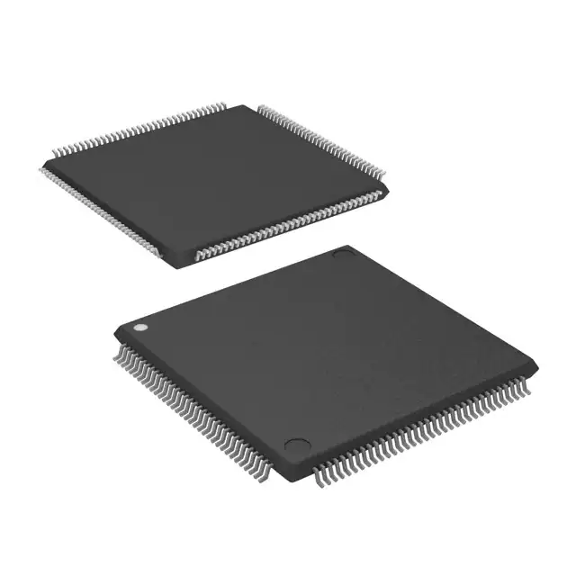
Package Information
Plastic Package
144-Pin LQFP, 20 x 20 mm, 0.5 mm pitch
100-Pin LQFP, 14 x 14 mm, 0.5 mm pitch
Ordering Information
See Table 2 on page 6
1
i.MX RT1020 introduction
The i.MX RT1020 is a processor of i.MX RT family
featuring NXP’s advanced implementation of the Arm®
Cortex®-M7 core, which operates at speeds up to 500
MHz to provide high CPU performance and real-time
response.
The i.MX RT1020 processor has 256 KB on-chip RAM,
which can be flexibly configured as TCM or
general-purpose on-chip RAM. The i.MX RT1020
integrates advanced power management module with
DCDC and LDO that reduces complexity of external
power supply and simplifies power sequencing. The
i.MX RT1020 also provides various memory interfaces,
including SDRAM, RAW NAND FLASH, NOR
FLASH, SD/eMMC, Quad SPI, and a wide range of
connectivity interfaces including UART, SPI, I2C, USB,
and CAN; for connecting peripherals including WLAN,
Bluetooth™, and GPS. The i.MX RT1020 also has rich
1. i.MX RT1020 introduction . . . . . . . . . . . . . . . . . . . . . . . . 1
1.1. Features . . . . . . . . . . . . . . . . . . . . . . . . . . . . . . . . 2
1.2. Ordering information . . . . . . . . . . . . . . . . . . . . . . . 6
2. Architectural overview . . . . . . . . . . . . . . . . . . . . . . . . . . . 9
2.1. Block diagram . . . . . . . . . . . . . . . . . . . . . . . . . . . . 9
3. Modules list . . . . . . . . . . . . . . . . . . . . . . . . . . . . . . . . . . 10
3.1. Special signal considerations . . . . . . . . . . . . . . . 16
3.2. Recommended connections for unused analog
interfaces . . . . . . . . . . . . . . . . . . . . . . . . . . . . . . . 17
4. Electrical characteristics . . . . . . . . . . . . . . . . . . . . . . . . 18
4.1. Chip-level conditions . . . . . . . . . . . . . . . . . . . . . . 18
4.2. System power and clocks . . . . . . . . . . . . . . . . . . 25
4.3. I/O parameters . . . . . . . . . . . . . . . . . . . . . . . . . . 30
4.4. System modules . . . . . . . . . . . . . . . . . . . . . . . . . 36
4.5. External memory interface . . . . . . . . . . . . . . . . . 41
4.6. Audio . . . . . . . . . . . . . . . . . . . . . . . . . . . . . . . . . . 51
4.7. Analog . . . . . . . . . . . . . . . . . . . . . . . . . . . . . . . . . 54
4.8. Communication interfaces . . . . . . . . . . . . . . . . . . 61
4.9. Timers . . . . . . . . . . . . . . . . . . . . . . . . . . . . . . . . . 73
5. Boot mode configuration . . . . . . . . . . . . . . . . . . . . . . . . 75
5.1. Boot mode configuration pins . . . . . . . . . . . . . . . 75
5.2. Boot device interface allocation . . . . . . . . . . . . . . 75
6. Package information and contact assignments . . . . . . . 81
6.1. 20 x 20 mm package information . . . . . . . . . . . . 81
6.2. 14 x 14 mm package information . . . . . . . . . . . . 90
7. Revision history . . . . . . . . . . . . . . . . . . . . . . . . . . . . . . . 97
Legal information . . . . . . . . . . . . . . . . . . . . . . . . . . . . . . 98
NXP reserves the right to change the production detail specifications as may be required
to permit improvements in the design of its products.
© 2018-2022 NXP B.V.
�i.MX RT1020 introduction
audio features, including SPDIF and I2S audio interface. Various analog IP integration, including ADC,
analog comparator, temperature sensor, etc.
The i.MX RT1020 is specifically useful for applications such as:
• Industrial
• Motor Control
• Home Appliance
• IoT
1.1
Features
The i.MX RT1020 processors are based on Arm Cortex-M7 Core™ Platform, which has the following
features:
• Supports single Arm Cortex-M7 with:
— 16 KB L1 Instruction Cache
— 16 KB L1 Data Cache
— Full featured Floating Point Unit (FPU) with support of the VFPv5 architecture
— Support the Armv7-M Thumb instruction set
• Integrated MPU, up to 16 individual protection regions
• Up to 256 KB I-TCM and D-TCM in total
• Target frequency of 500 MHz
• Cortex M7 CoreSight™ components integration for debug
• Frequency of the core, as per Table 11, "Operating ranges," on page 21.
The SoC-level memory system consists of the following additional components:
— Boot ROM (96 KB)
— On-chip RAM (256 KB)
– Configurable RAM size up to 256 KB shared with CM7 TCM
• External memory interfaces:
— 8/16-bit SDRAM, up to SDRAM-133
— 8/16-bit SLC NAND FLASH, with ECC handled in software
— SD/eMMC
— SPI NOR/NAND FLASH
— Parallel NOR FLASH with XIP support
— Single/Dual channel Quad SPI FLASH with XIP support
• Timers and PWMs:
— Two General Programmable Timers
– 4-channel generic 32-bit resolution timer
– Each support standard capture and compare operation
— Four Periodical Interrupt Timers
i.MX RT1020 Crossover Processors for Consumer Products, Rev. 3.1, 03/2022
2
NXP Semiconductors
�i.MX RT1020 introduction
– Generic 32-bit resolution timer
– Periodical interrupt generation
— Two Quad Timers
– 4-channel generic 16-bit resolution timer each
– Each support standard capture and compare operation
– Quadrature decoder integrated
— Two FlexPWMs
– Up to 12 individual PWM channels per each
– 16-bit resolution PWM suitable for Motor Control applications
— Two Quadrature Encoders/Decoders
Each i.MX RT1020 processor enables the following interfaces to external devices (some of them are
multiplexed and not available simultaneously):
• Audio:
— S/PDIF input and output
— Three synchronous audio interface (SAI) modules supporting I2S, AC97, TDM, and
codec/DSP interfaces
— MQS interface for medium quality audio via GPIO pads
• Connectivity:
— One USB 2.0 OTG controller with integrated PHY interface
— Two Ultra Secure Digital Host Controller (uSDHC) interfaces
– MMC 4.5 compliance support up to 100 MB/sec
– SD/SDIO 3.0 compliance with 200 MHz SDR signaling to support up to 100 MB/sec
– Support for SDXC (extended capacity)
— One 10/100 M Ethernet controller with IEEE1588 supported
— Eight universal asynchronous receiver/transmitter (UARTs) modules
— Four I2C modules
— Four SPI modules
— Two FlexCAN modules
• GPIO and Pin Multiplexing:
— General-purpose input/output (GPIO) modules with interrupt capability
— Input/output multiplexing controller (IOMUXC) to provide centralized pad control
— 96 GPIOs for 144-pin LQFP package, 57 GPIOs for 100-pin LQFP package
— One FlexIO
The i.MX RT1020 processors integrate Analog module:
— Two Analog-Digital-Converters (ADC), up to 19 channels
— Four Analog Comparators (ACMP)
The i.MX RT1020 processors integrate advanced power management unit and controllers:
i.MX RT1020 Crossover Processors for Consumer Products, Rev. 3.1, 03/2022
NXP Semiconductors
3
�i.MX RT1020 introduction
•
•
•
Full PMIC integration, including on-chip DCDC and LDOs
Temperature sensor with programmable trip points
GPC hardware power management controller
The i.MX RT1020 processors support the following system debug:
• Arm CortexM7 CoreSight debug and trace architecture
• Trace Port Interface Unit (TPIU) to support off-chip real-time trace
• Support for 5-pin (JTAG) and SWD debug interfaces selected by eFuse
Security functions are enabled and accelerated by the following hardware:
• High Assurance Boot (HAB)
• Data Co-Processor (DCP):
— AES-128, ECB, and CBC mode
— SHA-1 and SHA-256
— CRC-32
• Bus Encryption Engine (BEE)
— AES-128, ECB, and CTR mode
— On-the-fly QSPI Flash decryption
• True random number generation (TRNG)
• Secure Non-Volatile Storage (SNVS)
— Secure real-time clock (RTC)
— Zero Master Key (ZMK)
• Secure JTAG Controller (SJC)
Table 1 demonstrates the comparison between 100 LQFP and 144 LQFP package.
Table 1. The comparison between 100 LQFP and 144 LQFP package
144 LQFP
100 LQFP
RAM/KB
256
256
USB OTG
1
1
ENET port
MII/RMII
RMII
KPP number
8x8
4x4
SEMC
Yes
No
SPDIF
Yes
Yes
uSDHC1
2
1
FlexIO
32
22
GPIO
96
57
FlexPWM Channel
24
16
i.MX RT1020 Crossover Processors for Consumer Products, Rev. 3.1, 03/2022
4
NXP Semiconductors
�i.MX RT1020 introduction
Table 1. The comparison between 100 LQFP and 144 LQFP package (continued)
1
144 LQFP
100 LQFP
XBAR IN/OUT
16
9
SAI
3
3
ACMP
4
4
ADC channel
19
10
FLEXCAN
2
2
I2C
4
4
LPUART
8
8
FlexSPI
1
1
LPSPI
4
4
SD is 3.3 V in the 100 LQFP package, while it supports both 3.3 V and 1.8 V in the 144 LQFP package.
NOTE
The actual feature set depends on the part numbers as described in Table 2.
Functions such as display and camera interfaces, connectivity interfaces,
and security features are not offered on all derivatives.
i.MX RT1020 Crossover Processors for Consumer Products, Rev. 3.1, 03/2022
NXP Semiconductors
5
�i.MX RT1020 introduction
1.2
Ordering information
Table 2 provides examples of orderable part numbers covered by this data sheet.
Table 2. Ordering information
Part Number
Feature
Package
Junction
Temperature Tj (C)
MIMXRT1021DAF5A
Features supports:
• 500 MHz, consumer grade for general
purpose
• 256K RAM
• CAN x2
• Ethernet
• eMMC 4.5/SD 3.0 x1
• USB OTG x1
• SAI x3
• SPDIF x1
• Timer x2
• PWM x2
• UART x8
• I2C x4
• SPI x4
• ADC x2
• ACMP x4
• 57 GPIOs
14 x 14 mm, 0.5 mm pitch,
100-pin LQFP
0 to +95
MIMXRT1021DAG5A
Features supports:
• 500 MHz, consumer grade for general
purpose
• 256K RAM
• CAN x2
• Ethernet
• eMMC 4.5/SD 3.0 x2
• USB OTG x1
• SAI x3
• SPDIF x1
• Timer x2
• PWM x2
• UART x8
• I2C x4
• SPI x4
• ADC x2
• ACMP x4
• 96 GPIOs
20 x 20 mm, 0.5 mm pitch,
144-pin LQFP
0 to +95
i.MX RT1020 Crossover Processors for Consumer Products, Rev. 3.1, 03/2022
6
NXP Semiconductors
�i.MX RT1020 introduction
Table 2. Ordering information (continued)
Part Number
Feature
Package
Junction
Temperature Tj (C)
MIMXRT1021DAF5B
Features supports:
• 500 MHz, consumer grade for general
purpose
• 256K RAM
• CAN x2
• Ethernet
• eMMC 4.5/SD 3.0 x1
• USB OTG x1
• SAI x3
• SPDIF x1
• Timer x2
• PWM x2
• UART x8
• I2C x4
• SPI x4
• ADC x2
• ACMP x4
• 57 GPIOs
14 x 14 mm, 0.5 mm pitch,
100-pin LQFP
0 to +95
MIMXRT1021DAG5B
Features supports:
• 500 MHz, consumer grade for general
purpose
• 256K RAM
• CAN x2
• Ethernet
• eMMC 4.5/SD 3.0 x2
• USB OTG x1
• SAI x3
• SPDIF x1
• Timer x2
• PWM x2
• UART x8
• I2C x4
• SPI x4
• ADC x2
• ACMP x4
• 96 GPIOs
20 x 20 mm, 0.5 mm pitch,
144-pin LQFP
0 to +95
Figure 1 describes the part number nomenclature so that characteristics of a specific part number can be
identified (for example, cores, frequency, temperature grade, fuse options, and silicon revision). The
primary characteristic which describes which data sheet applies to a specific part is the temperature grade
(junction) field.
Ensure to have the proper data sheet for specific part by verifying the temperature grade (junction) field
and matching it to the proper data sheet. If there are any questions, visit the web page nxp.com/IMXRT or
contact an NXP representative for details.
i.MX RT1020 Crossover Processors for Consumer Products, Rev. 3.1, 03/2022
NXP Semiconductors
7
�i.MX RT1020 introduction
M
IMX
XX
@
##
%
+
VV
$
A
Qualification Level
M
Silicon Rev
A
Prototype Samples
P
A0
A
Mass Production
M
A1
B
Special
S
Core Frequency
$
400 MHz
4
500 MHz
5
600 MHz
6
Part # series
i.MX RT
XX
RT
Family
@
First Generation RT family
1
Reserved
Package Type
2-8
VV
225MAPBGA, 13 x 13 mm, 0.8 mm pitch
VN
Sub-Family
##
196MAPBGA, 12 x 12 mm, 0.8 mm pitch
VJ
RT101x
01
196MAPBGA, 10 x 10 mm, 0.65 mm pitch
VL
RT102x
02
169MAPBGA, 11 x 11 mm, 0.8 mm pitch
JM
RT104x
04
169MAPBGA, 9 x 9 mm, 0.65 mm pitch
FP
RT105x
05
144LQFP, 20 x 20 mm, 0.5 mm pitch
AG
RT106x
06
Tie
%
Standard Feature
1
Full Feature
2
100LQFP, 14 x 14 mm, 0.5 mm pitch
AF
80LQFP, 12 x 12 mm, 0.5 mm pitch
AE
4MB Flash SIP
4
Enhanced Feature
5
Temperature (Tj)
+
Far Field AFE
A
Consumer: 0 to + 95 °C
D
Facial Recognition
F
Industrial: -40 to +105 °C
C
Local Voice Control (audio input models)
L
Extended Industrial: -40 to +125 eC
X
Local Voice Control (text input models)
S
Figure 1. Part number nomenclature—i.MX RT10XX family
i.MX RT1020 Crossover Processors for Consumer Products, Rev. 3.1, 03/2022
8
NXP Semiconductors
�Architectural overview
2
Architectural overview
The following subsections provide an architectural overview of the i.MX RT1020 processor system.
2.1
Block diagram
Figure 2 shows the functional modules in the i.MX RT1020 processor system1.
System Control
CPU Platform
Connectivity
ARM Cortex-M7
eMMC 4.5 / SD 3.0 x2
Secure JTAG
PLL / OSC
16 KB D-cache
16 KB I-cache
RTC and Reset
FPU
UART x8
NVIC
MPU
Enhanced DMA
8 x 8 Keypad
Up to 256 KB TCM
IOMUX
I2C x4
GP Timer x6
Quadrature ENC x2
SPI x4
External Memory
QuadTimer
(4-Channel) x2
FlexPWM
(12-Channel) x2
Watch Dog x4
Internal Memory
256 KB OCRAM
shared with TCM
FlexSPI (dual-Channel QuadSPI
NAND and NOR, Octal Flash, and RAM)
GPIO
I2S / SAI x3
External Memory Controller
8/16 bit SDRAM
Parallel NOR Flash
NAND Flash
PSRAM
10 / 100 ENET
with IEEE 1588 x1
HAB
Power Management
FlexCAN x2
USB2.0 OTG with PHY
Security
96 KB ROM
S/PDIF Tx / Rx
DCDC
ADC
Ciphers
RNG
Secure RTC
eFuse
LDO
Temp Monitor
ADC x2
ACMP x4
.
Figure 2. i.MX RT1020 system block diagram
1. Some modules shown in this block diagram are not offered on all derivatives. See Table 2 for details.
i.MX RT1020 Crossover Processors for Consumer Products, Rev. 3.1, 03/2022
NXP Semiconductors
9
�Modules list
3
Modules list
The i.MX RT1020 processors contain a variety of digital and analog modules. Table 3 describes these
modules in alphabetical order.
Table 3. i.MX RT1020 modules list
Block mnemonic
Block name
Subsystem
Brief description
ACMP1
ACMP2
ACMP3
ACMP4
Analog Comparator
Analog
The comparator (CMP) provides a circuit for comparing
two analog input voltages. The comparator circuit is
designed to operate across the full range of the supply
voltage (rail-to-rail operation).
ADC1
ADC2
Analog to Digital
Converter
Analog
The ADC is a 12-bit general purpose analog to digital
converter.
AOI
And-Or-Inverter
Cross Trigger
The AOI provides a universal boolean function
generator using a four team sum of products expression
with each product term containing true or complement
values of the four selected inputs (A, B, C, D).
Arm
Arm Platform
Arm
The Arm Core Platform includes 1x Cortex-M7 core. It
also includes associated sub-blocks, such as Nested
Vectored Interrupt Controller (NVIC), Floating-Point
Unit (FPU), Memory Protection Unit (MPU), and
CoreSight debug modules.
BEE
Bus Encryption Engine
Security
On-The-Fly FlexSPI Flash Decryption
CCM
GPC
SRC
Clocks, Resets, and These modules are responsible for clock and reset
Clock Control Module,
Power Control
distribution in the system, and also for the system
General Power
power management.
Controller, System Reset
Controller
CSU
Central Security Unit
Security
The Central Security Unit (CSU) is responsible for
setting comprehensive security policy within the i.MX
RT1020 platform.
DAP
Debug Access Port
System Control
Peripherals
The DAP provides real-time access for the debugger
without halting the core to:
• System memory and peripheral registers
• All debug configuration registers
The DAP also provides debugger access to JTAG scan
chains. The DAP module is internal to the Cortex-M7
Core Platform.
DCDC
DCDC Converter
Analog
The DCDC module is used for generating power supply
for core logic. Main features are:
• Adjustable high efficiency regulator
• Supports 3.3 V input voltage
• Supports nominal run and low power standby modes
• Supports at 0.9 ~ 1.3 V output in run mode
• Supports at 0.9 ~ 1.0 V output in standby mode
• Over current and over voltage detection
i.MX RT1020 Crossover Processors for Consumer Products, Rev. 3.1, 03/2022
10
NXP Semiconductors
�Modules list
Table 3. i.MX RT1020 modules list (continued)
Block mnemonic
Block name
Subsystem
Brief description
eDMA
enhanced Direct Memory System Control
Access
Peripherals
There is an enhanced DMA (eDMA) engine and two
DMA_MUX.
• The eDMA is a 32 channel DMA engine, which is
capable of performing complex data transfers with
minimal intervention from a host processor.
• The DMA_MUX is capable of multiplexing up to 128
DMA request sources to the 32 DMA channels of
eDMA.
ENC
Quadrature
Encoder/Decoder
Timer Peripherals
The enhanced quadrature encoder/decoder module
provides interfacing capability to position/speed
sensors. There are five input signals: PHASEA,
PHASEB, INDEX, TRIGGER, and HOME. This module
is used to decode shaft position, revolution count, and
speed.
ENET
Ethernet Controller
Connectivity
Peripherals
The Ethernet Media Access Controller (MAC) is
designed to support 10/100 Mbit/s Ethernet/IEEE 802.3
networks. An external transceiver interface and
transceiver function are required to complete the
interface to the media. The module has dedicated
hardware to support the IEEE 1588 standard. See the
ENET chapter of the reference manual for details.
EWM
External Watchdog
Monitor
Timer Peripherals
The EWM modules is designed to monitor external
circuits, as well as the software flow. This provides a
back-up mechanism to the internal WDOG that can
reset the system. The EWM differs from the internal
WDOG in that it does not reset the system. The EWM,
if allowed to time-out, provides an independent trigger
pin that when asserted resets or places an external
circuit into a safe mode.
FLEXCAN1
FLEXCAN2
Flexible Controller Area
Network
Connectivity
Peripherals
The CAN protocol was primarily, but not only, designed
to be used as a vehicle serial data bus, meeting the
specific requirements of this field: real-time processing,
reliable operation in the Electromagnetic interference
(EMI) environment of a vehicle, cost-effectiveness and
required bandwidth. The FlexCAN module is a full
implementation of the CAN protocol specification,
Version 2.0 B, which supports both standard and
extended message frames.
FlexIO1
Flexible Input/output
Connectivity and
Communications
The FlexIO is capable of supporting a wide range of
protocols including, but not limited to: UART, I2C, SPI,
I2S, camera interface, display interface, PWM
waveform generation, etc. The module can remain
functional when the chip is in a low power mode
provided the clock it is using remain active.
i.MX RT1020 Crossover Processors for Consumer Products, Rev. 3.1, 03/2022
NXP Semiconductors
11
�Modules list
Table 3. i.MX RT1020 modules list (continued)
Block mnemonic
Block name
Subsystem
Brief description
FlexPWM1
FlexPWM2
Pulse Width Modulation
Timer Peripherals
The pulse-width modulator (PWM) contains four PWM
sub-modules, each of which is set up to control a single
half-bridge power stage. Fault channel support is
provided. The PWM module can generate various
switching patterns, including highly sophisticated
waveforms.
FlexRAM
RAM
Memories
The i.MX RT1020 has 256 KB of on-chip RAM which
could be flexible allocated to I-TCM, D-TCM, and
on-chip RAM (OCRAM) in a 32 KB granularity. The
FlexRAM is the manager of the 256 KB on-chip RAM
array. Major functions of this blocks are: interfacing to
I-TCM and D-TCM of Arm core and OCRAM controller;
dynamic RAM arrays allocation for I-TCM, D-TCM, and
OCRAM.
FlexSPI
Quad Serial Peripheral
Interface
Connectivity and
Communications
FlexSPI acts as an interface to one or two external
serial flash devices, each with up to four bidirectional
data lines.
GPIO1
GPIO2
GPIO3
GPIO5
General Purpose I/O
Modules
System Control
Peripherals
Used for general purpose input/output to external ICs.
Each GPIO module supports up to 32 bits of I/O.
GPT1
GPT2
General Purpose Timer
Timer Peripherals
Each GPT is a 32-bit “free-running” or “set and forget”
mode timer with programmable prescaler and compare
and capture register. A timer counter value can be
captured using an external event and can be configured
to trigger a capture event on either the leading or trailing
edges of an input pulse. When the timer is configured to
operate in “set and forget” mode, it is capable of
providing precise interrupts at regular intervals with
minimal processor intervention. The counter has output
compare logic to provide the status and interrupt at
comparison. This timer can be configured to run either
on an external clock or on an internal clock.
KPP
Keypad Port
Human Machine
Interfaces
The KPP is a 16-bit peripheral that can be used as a
keypad matrix interface or as general purpose
input/output (I/O). It supports 8 x 8 external key pad
matrix. Main features are:
• Multiple-key detection
• Long key-press detection
• Standby key-press detection
• Supports a 2-point and 3-point contact key matrix
LPI2C1
LPI2C2
LPI2C3
LPI2C4
Low Power
Inter-integrated Circuit
Connectivity and
Communications
The LPI2C is a low power Inter-Integrated Circuit (I2C)
module that supports an efficient interface to an I2C bus
as a master.
The I2C provides a method of communication between
a number of external devices. More detailed
information, see Section 4.8.2, LPI2C module timing
parameters.
i.MX RT1020 Crossover Processors for Consumer Products, Rev. 3.1, 03/2022
12
NXP Semiconductors
�Modules list
Table 3. i.MX RT1020 modules list (continued)
Block mnemonic
Block name
Subsystem
Brief description
LPSPI1
LPSPI2
LPSPI3
LPSPI4
Low Power Serial
Peripheral Interface
Connectivity and
Communications
The LPSPI is a low power Serial Peripheral Interface
(SPI) module that support an efficient interface to an
SPI bus as a master and/or a slave.
• It can continue operating while the chip is in stop
modes, if an appropriate clock is available
• Designed for low CPU overhead, with DMA off
loading of FIFO register access
LPUART1
LPUART2
LPUART3
LPUART4
LPUART5
LPUART6
LPUART7
LPUART8
UART Interface
Connectivity
Peripherals
Each of the UART modules support the following serial
data transmit/receive protocols and configurations:
• 7- or 8-bit data words, 1 or 2 stop bits, programmable
parity (even, odd or none)
• Programmable baud rates up to 20 Mbps.
MQS
Medium Quality Sound
Multimedia
Peripherals
MQS is used to generate 2-channel medium quality
PWM-like audio via two standard digital GPIO pins.
QuadTimer1
QuadTimer2
QuadTimer
Timer Peripherals
The quad-timer provides four time channels with a
variety of controls affecting both individual and
multi-channel features.Specific features include
up/down count, cascading of counters, programmable
module, count once/repeated, counter preload,
compare registers with preload, shared use of input
signals, prescaler controls, independent
capture/compare, fault input control, programmable
input filters, and multi-channel synchronization.
ROMCP
ROM Controller with
Patch
Memories and
The ROMCP acts as an interface between the Arm
Memory Controllers advanced high-performance bus and the ROM. The
on-chip ROM is only used by the Cortex-M7 core during
boot up. Size of the ROM is 96 KB.
RTC OSC
Real Time Clock
Oscillator
Clock Sources and
Control
The RTC OSC provides the clock source for the
Real-Time Clock module. The RTC OSC module, in
conjunction with an external crystal, generates a 32.768
kHz reference clock for the RTC.
RTWDOG
Watch Dog
Timer Peripherals
The RTWDG module is a high reliability independent
timer that is available for system to use. It provides a
safety feature to ensure software is executing as
planned and the CPU is not stuck in an infinite loop or
executing unintended code. If the WDOG module is not
serviced (refreshed) within a certain period, it resets the
MCU. Windowed refresh mode is supported as well.
SAI1
SAI2
SAI3
Synchronous Audio
Interface
Multimedia
Peripherals
The SAI module provides a synchronous audio
interface (SAI) that supports full duplex serial interfaces
with frame synchronization, such as I2S, AC97, TDM,
and codec/DSP interfaces.
SA-TRNG
Standalone True Random Security
Number Generator
The SA-TRNG is hardware accelerator that generates
a 512-bit entropy as needed by an entropy consuming
module or by other post processing functions.
i.MX RT1020 Crossover Processors for Consumer Products, Rev. 3.1, 03/2022
NXP Semiconductors
13
�Modules list
Table 3. i.MX RT1020 modules list (continued)
Block mnemonic
Block name
Subsystem
Brief description
SEMC
Smart External Memory
Controller
Memory and
Memory Controller
The SEMC is a multi-standard memory controller
optimized for both high-performance and low pin-count.
It can support multiple external memories in the same
application with shared address and data pins. The
interface supported includes SDRAM, NOR Flash,
SRAM, and NAND Flash, as well as 8080 display
interface.
SJC
System JTAG Controller
System Control
Peripherals
The SJC provides JTAG interface, which complies with
JTAG TAP standards, to internal logic. The i.MX
RT1020 processors use JTAG port for production,
testing, and system debugging. In addition, the SJC
provides BSR (Boundary Scan Register) standard
support, which complies with IEEE1149.1 and
IEEE1149.6 standards.
The JTAG port is accessible during platform initial
laboratory bring-up, for manufacturing tests and
troubleshooting, as well as for software debugging by
authorized entities. The i.MX RT1020 SJC incorporates
three security modes for protecting against
unauthorized accesses. Modes are selected through
eFUSE configuration.
SNVS
Secure Non-Volatile
Storage
Security
Secure Non-Volatile Storage, including Secure Real
Time Clock, Security State Machine, and Master Key
Control.
SPDIF
Sony Philips Digital
Interconnect Format
Multimedia
Peripherals
A standard audio file transfer format, developed jointly
by the Sony and Phillips corporations. Has Transmitter
and Receiver functionality.
Temp Monitor
Temperature Monitor
Analog
The temperature sensor implements a temperature
sensor/conversion function based on a
temperature-dependent voltage to time conversion.
USBO2
Universal Serial Bus 2.0
Connectivity
Peripherals
USBO2 (USB OTG1) contains:
• One high-speed OTG 2.0 module with integrated HS
USB PHY
• Support eight Transmit (TX) and eight Receive (Rx)
endpoints, including endpoint 0
i.MX RT1020 Crossover Processors for Consumer Products, Rev. 3.1, 03/2022
14
NXP Semiconductors
�Modules list
Table 3. i.MX RT1020 modules list (continued)
Block mnemonic
Block name
Subsystem
Brief description
uSDHC1
uSDHC2
Connectivity
SD/MMC and SDXC
Peripherals
Enhanced Multi-Media
Card / Secure Digital Host
Controller
i.MX RT1020 specific SoC characteristics:
All four MMC/SD/SDIO controller IPs are identical and
are based on the uSDHC IP. They are:
• Fully compliant with MMC command/response sets
and Physical Layer as defined in the Multimedia
Card System Specification, v4.5/4.2/4.3/4.4/4.41/
including high-capacity (size > 2 GB) cards HC
MMC.
• Fully compliant with SD command/response sets
and Physical Layer as defined in the SD Memory
Card Specifications, v3.0 including high-capacity
SDXC cards up to 2 TB.
• Fully compliant with SDIO command/response sets
and interrupt/read-wait mode as defined in the SDIO
Card Specification, Part E1, v3.0
Two ports support:
• 1-bit or 4-bit transfer mode specifications for SD and
SDIO cards up to UHS-I SDR104 mode (104 MB/s
max)
• 1-bit, 4-bit, or 8-bit transfer mode specifications for
MMC cards up to 52 MHz in both SDR and DDR
modes (104 MB/s max)
• 4-bit transfer mode specifications for eMMC chips up
to 100 MHz in HS200 mode (100 MB/s max)
WDOG1
WDOG2
Watch Dog
Timer Peripherals
The Watch Dog Timer supports two comparison points
during each counting period. Each of the comparison
points is configurable to evoke an interrupt to the Arm
core, and a second point evokes an external event on
the WDOG line.
XBAR
Cross BAR
Cross Trigger
Each crossbar switch is an array of muxes with shared
inputs. Each mux output provides one output of the
crossbar. The number of inputs and the number of
muxes/outputs are user configurable and registers are
provided to select which of the shared inputs are routed
to each output.
i.MX RT1020 Crossover Processors for Consumer Products, Rev. 3.1, 03/2022
NXP Semiconductors
15
�Modules list
3.1
Special signal considerations
Table 4 lists special signal considerations for the i.MX RT1020 processors. The signal names are listed in
alphabetical order.
The package contact assignments can be found in Section 6, Package information and contact
assignments.” Signal descriptions are provided in the i.MX RT1020 Reference Manual
(IMXRT1020RM).
Table 4. Special signal considerations
Signal name
Remarks
DCDC_PSWITCH
PAD is in DCDC_IN domain and connected the ground to bypass DCDC.
To enable DCDC function, assert to DCDC_IN with at least 1ms delay for DCDC_IN rising edge.
RTC_XTALI/RTC_XTALO
If the user wishes to configure RTC_XTALI and RTC_XTALO as an RTC oscillator, a 32.768 kHz
crystal, (100 k ESR, 10 pF load) should be connected between RTC_XTALI and RTC_XTALO.
Keep in mind the capacitors implemented on either side of the crystal are about twice the crystal
load capacitor. To hit the exact oscillation frequency, the board capacitors need to be reduced to
account for board and chip parasitics. The integrated oscillation amplifier is self biasing, but
relatively weak. Care must be taken to limit parasitic leakage from RTC_XTALI and RTC_XTALO
to either power or ground (>100 M). This will debias the amplifier and cause a reduction of
startup margin. Typically RTC_XTALI and RTC_XTALO should bias to approximately 0.5 V.
If it is desired to feed an external low frequency clock into RTC_XTALI the RTC_XTALO pin must
remain unconnected or driven with a complimentary signal. The logic level of this forcing clock
should not exceed VDD_SNVS_CAP level and the frequency should be