Freescale Semiconductor, Inc.
Data Sheet: Technical Data
K24P121M120SF5
Rev 2, 08/2014
Kinetis K24F Sub-Family 256 KB
Flash Data Sheet
MK24FN256VDC12
120 MHz ARM® Cortex®-M4-based Microcontroller with FPU
The K24F product family features high memory densities, low
power capabilities, and optimized integration. It shares the
comprehensive enablement and scalability of the Kinetis family.
This product offers:
• 1-1 flash to RAM ratio, with 256 KB of embedded flash and
256 KB of embedded RAM to support application with high
RAM density requirements.
• USB LS/FS OTG 2.0 with embedded 3.3 V, 120 mA LDO
voltage regulator and USB device crystal-less operation.
• Run power consumption down to 220 μA/MHz. Static
power consumption down to 3.68 μA with full state
retention and 5 μs wakeup. Lowest Static mode down to
173 nA
121 XFBGA
8 x 8 x 0.5 mm Pitch 0.65 mm
Performance
• Up to 120 MHz ARM® Cortex®-M4 core with DSP
instructions and floating point unit
Communication interfaces
• USB full-/low-speed On-the-Go controller
• USB Device Charger detect (USBDCD)
• Three SPI modules
Memories and memory interfaces
• Three I2C modules
• Up to 256 KB program flash memory and 256 KB RAM
• Six UART modules
• Serial programming interface (EzPort)
• I2S module
• Pre-programmed Kinetis flashloader for one-time, inTimers
system factory programming
• Two 8-channel motor control/general purpose/PWM
System peripherals
timers
• Multiple low-power modes, low-leakage wakeup unit
• Two 2-channel quadrature decoder/general purpose
• 16-channel DMA controller
timers
• External watchdog monitor
• Periodic interrupt timers and 16-bit low power timer
• Software watchdog
• Carrier modulator transmitter
• Real-time clock
Clocks
• Programmable delay block
• 3 to 32 MHz and 32 kHz crystal oscillator
• Multipurpose clock generator with FLL and PLL
Security and integrity modules
• 32 kHz, and 4 MHz internal reference clock
• Hardware CRC module
• 48 MHz internal reference
• 128-bit unique identification (ID) number per chip
Analog modules
• Two 16-bit SAR ADCs
• 12-bit DAC
• Two analog comparators (CMP)
• Voltage reference
Operating Characteristics
• Voltage range: 1.71 to 3.6 V
• Flash write voltage range: 1.71 to 3.6 V
• Temperature range (ambient): –40 to 105 °C
Freescale reserves the right to change the detail specifications as may be required to
permit improvements in the design of its products. © 2014 Freescale Semiconductor,
Inc. All rights reserved.
�Ordering Information 1
Part Number
MK24FN256VDC12
Memory
Maximum number of I\O's
Flash
SRAM (KB)
256 KB
256
83
1. To confirm current availability of ordererable part numbers, go to http://www.freescale.com and perform a part number
search.
Related Resources
Type
Description
Resource
Selector
Guide
The Freescale Solution Advisor is a web-based tool that features
interactive application wizards and a dynamic product selector.
Solution Advisor
Product Brief
The Product Brief contains concise overview/summary information to
enable quick evaluation of a device for design suitability.
K60PB1
Reference
Manual
The Reference Manual contains a comprehensive description of the
structure and function (operation) of a device.
K24P121M120SF5RM 1
Data Sheet
The Data Sheet includes electrical characteristics and signal
connections.
This document
Package
drawing
Package dimensions are provided in package drawings.
XFBGA 121-pin: 98ASA00595D1
1. To find the associated resource, go to http://www.freescale.com and perform a search using this term.
2
Freescale Semiconductor, Inc.
Kinetis K24F Sub-Family 256 KB Flash Data Sheet, Rev2, 08/2014.
�Kinetis K24 Family
ARM ® Cortex™-M4
Core
System
Memories and Memory Interfaces
Internal
and external
watchdogs
Program
flash
Serial
programming
interface
Debug
interfaces
DSP
DMA
Interrupt
controller
Floating
point
Low-leakage
wakeup
RAM
Clocks
Phaselocked loop
Frequencylocked loop
Low/high
frequency
oscillators
Internal
reference
clocks
Communication Interfaces
Security
Analog
Timers
CRC
16-bit ADC
x2
Timers
x2 (8ch)
x2 (2ch)
I C
x3
I S
x1
Random
number
generator
Analog
comparator
x2
Programmable
delay block
UART
x6
USB OTG
LS/FS
6-bit DAC
x2
Periodic
interrupt
timers
SPI
x3
USB LS/FS
transceiver
12-bit DAC
x1
Low power
timer
USB charger
detect
Voltage
reference
Independent
real-time
clock
USB voltage
regulator
and Integrity
2
Human-Machine
Interface (HMI)
2
GPIO
Carrier
Modulator
Transmitter
Figure 1. K24 block diagram
Kinetis K24F Sub-Family 256 KB Flash Data Sheet, Rev2, 08/2014.
3
Freescale Semiconductor, Inc.
�Table of Contents
1 Ratings.................................................................................... 5
1.1 Thermal handling ratings................................................. 5
1.2 Moisture handling ratings................................................ 5
1.3 ESD handling ratings....................................................... 5
1.4 Voltage and current operating ratings............................. 5
2 General................................................................................... 6
2.1 AC electrical characteristics.............................................6
2.2 Nonswitching electrical specifications..............................6
2.2.1 Voltage and current operating requirements....... 6
2.2.2 LVD and POR operating requirements................7
2.2.3 Voltage and current operating behaviors.............8
2.2.4 Power mode transition operating behaviors........ 10
2.2.5 Power consumption operating behaviors............ 10
2.2.6 EMC radiated emissions operating behaviors..... 15
2.2.7 Designing with radiated emissions in mind..........16
2.2.8 Capacitance attributes.........................................16
2.3 Switching specifications...................................................16
2.3.1 Device clock specifications..................................16
2.3.2 General switching specifications......................... 17
2.4 Thermal specifications..................................................... 18
2.4.1 Thermal operating requirements......................... 18
2.4.2 Thermal attributes................................................18
3 Peripheral operating requirements and behaviors.................. 19
3.1 Core modules.................................................................. 19
3.1.1 JTAG electricals.................................................. 20
3.2 System modules.............................................................. 23
3.3 Clock modules................................................................. 23
3.3.1 MCG specifications..............................................23
3.3.2 IRC48M specifications.........................................25
3.3.3 Oscillator electrical specifications........................26
3.3.4 32 kHz oscillator electrical characteristics........... 28
3.4 Memories and memory interfaces................................... 29
3.4.1 Flash electrical specifications.............................. 29
3.4.2 EzPort switching specifications........................... 30
3.5 Analog............................................................................. 31
3.5.1 ADC electrical specifications............................... 31
3.5.2 CMP and 6-bit DAC electrical specifications....... 36
3.5.3 12-bit DAC electrical characteristics....................38
3.5.4 Voltage reference electrical specifications.......... 41
4
Freescale Semiconductor, Inc.
3.6 Timers..............................................................................42
3.7 Communication interfaces............................................... 42
3.7.1 USB electrical specifications............................... 42
3.7.2 USB DCD electrical specifications.......................43
3.7.3 USB VREG electrical specifications.................... 43
3.7.4 DSPI switching specifications (limited voltage
range).................................................................. 44
3.7.5 DSPI switching specifications (full voltage
range).................................................................. 45
3.7.6 Inter-Integrated Circuit Interface (I2C) timing...... 47
3.7.7 UART switching specifications............................ 49
3.7.8 I2S switching specifications.................................49
4 Dimensions............................................................................. 55
4.1 Obtaining package dimensions....................................... 55
5 Pinout...................................................................................... 55
5.1 K24 Signal Multiplexing and Pin Assignments.................55
5.2 Unused analog interfaces................................................ 60
5.3 K24 Pinouts..................................................................... 61
5.4 Ordering parts..................................................................62
5.4.1 Determining valid orderable parts........................62
5.5 Part identification............................................................. 63
5.5.1 Description...........................................................63
5.5.2 Format................................................................. 63
5.5.3 Fields................................................................... 63
5.5.4 Example...............................................................64
5.6 Terminology and guidelines.............................................64
5.6.1 Definition: Operating requirement........................64
5.6.2 Definition: Operating behavior............................. 65
5.6.3 Definition: Attribute.............................................. 65
5.6.4 Definition: Rating................................................. 65
5.6.5 Result of exceeding a rating................................ 66
5.6.6 Relationship between ratings and operating
requirements........................................................66
5.6.7
Guidelines for ratings and operating
requirements........................................................67
5.6.8 Definition: Typical value.......................................67
5.6.9 Typical value conditions...................................... 68
6 Revision History...................................................................... 69
Kinetis K24F Sub-Family 256 KB Flash Data Sheet, Rev2, 08/2014.
�Ratings
1 Ratings
1.1 Thermal handling ratings
Symbol
Description
Min.
Max.
Unit
Notes
TSTG
Storage temperature
–55
150
°C
1
TSDR
Solder temperature, lead-free
—
260
°C
2
Solder temperature, leaded
—
245
1. Determined according to JEDEC Standard JESD22-A103, High Temperature Storage Life.
2. Determined according to IPC/JEDEC Standard J-STD-020, Moisture/Reflow Sensitivity Classification for Nonhermetic
Solid State Surface Mount Devices.
1.2 Moisture handling ratings
Symbol
MSL
Description
Moisture sensitivity level
Min.
Max.
Unit
Notes
—
3
—
1
1. Determined according to IPC/JEDEC Standard J-STD-020, Moisture/Reflow Sensitivity Classification for Nonhermetic
Solid State Surface Mount Devices.
1.3 ESD handling ratings
Symbol
Description
Min.
Max.
Unit
Notes
VHBM
Electrostatic discharge voltage, human body model
-2000
+2000
V
1
VCDM
Electrostatic discharge voltage, charged-device
model
-500
+500
V
2
Latch-up current at ambient temperature of 70 °C
-100
+100
mA
3
ILAT
1. Determined according to JEDEC Standard JESD22-A114, Electrostatic Discharge (ESD) Sensitivity Testing Human
Body Model (HBM).
2. Determined according to JEDEC Standard JESD22-C101, Field-Induced Charged-Device Model Test Method for
Electrostatic-Discharge-Withstand Thresholds of Microelectronic Components.
3. Determined according to JEDEC Standard JESD78, IC Latch-Up Test.
1.4 Voltage and current operating ratings
Kinetis K24F Sub-Family 256 KB Flash Data Sheet, Rev2, 08/2014.
5
Freescale Semiconductor, Inc.
�General
Symbol
Description
Min.
Max.
Unit
VDD
Digital supply voltage
–0.3
3.8
V
IDD
Digital supply current
—
185
mA
VDIO
Digital input voltage (except RESET, EXTAL, and XTAL)
–0.3
VDD + 0.3
V
VAIO
Analog1,
–0.3
VDD + 0.3
V
ID
VDDA
RESET, EXTAL, and XTAL input voltage
Maximum current single pin limit (applies to all digital pins)
Analog supply voltage
–25.0
25
mA
VDD – 0.3
VDD + 0.3
V
VUSB0_DP
USB0_DP input voltage
–0.3
3.63
V
VUSB0_DM
USB0_DM input voltage
–0.3
3.63
V
RTC battery supply voltage
–0.3
3.8
V
VBAT
1. Analog pins are defined as pins that do not have an associated general purpose I/O port function.
2 General
2.1 AC electrical characteristics
Unless otherwise specified, propagation delays are measured from the 50% to the 50%
point, and rise and fall times are measured at the 20% and 80% points, as shown in the
following figure.
VIH
Input Signal
High
Low
80%
50%
20%
Midpoint1
Fall Time
VIL
Rise Time
The midpoint is VIL + (VIH - VIL) / 2
Figure 2. Input signal measurement reference
2.2 Nonswitching electrical specifications
6
Freescale Semiconductor, Inc.
Kinetis K24F Sub-Family 256 KB Flash Data Sheet, Rev2, 08/2014.
�General
2.2.1 Voltage and current operating requirements
Table 1. Voltage and current operating requirements
Symbol
Description
Min.
Max.
Unit
VDD
Supply voltage
1.71
3.6
V
VDDA
Analog supply voltage
1.71
3.6
V
VDD – VDDA VDD-to-VDDA differential voltage
–0.1
0.1
V
VSS – VSSA VSS-to-VSSA differential voltage
–0.1
0.1
V
1.71
3.6
V
0.7 × VDD
—
V
0.75 × VDD
—
V
• 2.7 V ≤ VDD ≤ 3.6 V
—
0.35 × VDD
V
• 1.71 V ≤ VDD ≤ 2.7 V
—
0.3 x VDD
V
0.06 × VDD
—
V
VBAT
VIH
RTC battery supply voltage
Input high voltage
• 2.7 V ≤ VDD ≤ 3.6 V
• 1.71 V ≤ VDD ≤ 2.7 V
VIL
Input low voltage
VHYS
Input hysteresis
IICIO
Analog1,
pin DC injection current — single pin
• VIN < VSS-0.3V (Negative current injection)
• VIN > VDD+0.3V (Positive current injection)
IICcont
Contiguous pin DC injection current —regional limit,
includes sum of negative injection currents or sum of
positive injection currents of 16 contiguous pins
• Negative current injection
• Positive current injection
VODPU
Open drain pullup voltage level
VRAM
VDD voltage required to retain RAM
VRFVBAT
Notes
VBAT voltage required to retain the VBAT register file
2
mA
-3
—
—
+3
-25
—
—
+25
VDD
VDD
V
1.2
—
V
VPOR_VBAT
—
V
mA
3
4
1. Analog pins are defined as pins that do not have an associated general purpose I/O port function. Additionally, EXTAL
and XTAL are analog pins.
2. All analog and I/O pins are internally clamped to VSS and VDD through ESD protection diodes. If VIN is less than
VIO_MIN or greater than VIO_MAX, a current limiting resistor is required. The negative DC injection current limiting
resistor is calculated as R=(VIO_MIN-VIN)/|IICIO|. The positive injection current limiting resistor is calculated as R=(VINVIO_MAX)/|IICIO|. Select the larger of these two calculated resistances if the pin is exposed to positive and negative
injection currents.
3. Open drain outputs must be pulled to VDD.
4. If VBAT is not used, the pin must be left floating.
Kinetis K24F Sub-Family 256 KB Flash Data Sheet, Rev2, 08/2014.
7
Freescale Semiconductor, Inc.
�General
2.2.2 LVD and POR operating requirements
Table 2. VDD supply LVD and POR operating requirements
Symbol
Description
Min.
Typ.
Max.
Unit
VPOR
Falling VDD POR detect voltage
0.8
1.1
1.5
V
VLVDH
Falling low-voltage detect threshold — high
range (LVDV=01)
2.48
2.56
2.64
V
Low-voltage warning thresholds — high range
1
VLVW1H
• Level 1 falling (LVWV=00)
2.62
2.70
2.78
V
VLVW2H
• Level 2 falling (LVWV=01)
2.72
2.80
2.88
V
VLVW3H
• Level 3 falling (LVWV=10)
2.82
2.90
2.98
V
VLVW4H
• Level 4 falling (LVWV=11)
2.92
3.00
3.08
V
—
80
—
mV
1.54
1.60
1.66
V
VHYSH
Low-voltage inhibit reset/recover hysteresis —
high range
VLVDL
Falling low-voltage detect threshold — low
range (LVDV=00)
1,
Low-voltage warning thresholds — low range
VLVW1L
• Level 1 falling (LVWV=00)
1.74
1.80
1.86
V
VLVW2L
• Level 2 falling (LVWV=01)
1.84
1.90
1.96
V
VLVW3L
• Level 3 falling (LVWV=10)
1.94
2.00
2.06
V
VLVW4L
• Level 4 falling (LVWV=11)
2.04
2.10
2.16
V
—
60
—
mV
VHYSL
Low-voltage inhibit reset/recover hysteresis —
low range
Notes
VBG
Bandgap voltage reference
0.97
1.00
1.03
V
tLPO
Internal low power oscillator period — factory
trimmed
900
1000
1100
μs
2
1. Rising threshold is the sum of falling threshold and hysteresis voltage
2. , The reset state of the LVD is low range threshold. To utilize the LVD for the specified VDD range, change the LVD
range to 'high range'.
Table 3. VBAT power operating requirements
Symbol
Description
VPOR_VBAT Falling VBAT supply POR detect voltage
Min.
Typ.
Max.
Unit
0.8
1.1
1.5
V
Notes
2.2.3 Voltage and current operating behaviors
Table 4. Voltage and current operating behaviors
Symbol
VOH
Description
Min.
Max.
Unit
Output high voltage — High drive pad
1
VDD – 0.5
8
Freescale Semiconductor, Inc.
Notes
—
V
Table continues on the next page...
Kinetis K24F Sub-Family 256 KB Flash Data Sheet, Rev2, 08/2014.
�General
Table 4. Voltage and current operating behaviors (continued)
Symbol
Description
• 2.7 V ≤ VDD ≤ 3.6 V, IOH = -20 mA
Min.
Max.
Unit
VDD – 0.5
—
V
Notes
• 1.71 V ≤ VDD ≤ 2.7 V, IOH = -10 mA
Output high voltage — Normal drive pad
IOHT
• 2.7 V ≤ VDD ≤ 3.6 V, IOH = -5 mA
VDD – 0.5
—
V
• 1.71 V ≤ VDD ≤ 2.7 V, IOH = -2.5 mA
VDD – 0.5
—
V
—
100
mA
VBAT – 0.5
—
V
VBAT – 0.5
—
V
—
100
mA
Output high current total for all ports
VOH_RTC_WA Output high voltage — normal drive pad
KEUP
1
• 2.7 V ≤ VBAT ≤ 3.6 V, IOH = -5 mA
• 1.71 V ≤ VBAT ≤ 2.7 V, IOH = -1.5 mA
IOH_RTC_WAK Output high current total for RTC_WAKEUP pins
EUP
VOL
Output low voltage — high drive pad
1
• 2.7 V ≤ VDD ≤ 3.6 V, IOL = 20 mA
—
0.5
V
• 1.71 V ≤ VDD ≤ 2.7 V, IOL = 10 mA
—
0.5
V
Output low voltage — normal drive pad
IOLT
• 2.7 V ≤ VDD ≤ 3.6 V, IOL = 5mA
—
0.5
V
• 1.71 V ≤ VDD ≤ 2.7 V, IOL = 2.5 mA
—
0.5
V
—
100
mA
—
0.5
V
—
0.5
V
—
100
mA
Output low current total for all ports
VOL_RTC_WA Output low voltage — normal drive pad
KEUP
1
• 2.7 V ≤ VBAT ≤ 3.6 V, IOL = 5mA
• 1.71 V ≤ VBAT ≤ 2.7 V, IOL = 1.5 mA
IOL_RTC_WAK Output low current total for RTC_WAKEUP pins
EUP
IIN
Input leakage current (per pin) for full temperature
range
—
1
μA
2
IIN
Input leakage current (per pin) at 25°C
—
0.025
μA
2
IIN_RTC_WAK Input leakage current (per RTC_WAKEUP pin) for full
temperature range
EUP
—
1
μA
IIN_RTC_WAK Input leakage current (per RTC_WAKEUP pin) at
25°C
EUP
—
0.025
μA
—
0.25
μA
—
0.25
μA
IOZ
Hi-Z (off-state) leakage current (per pin)
IOZ_RTC_WAK Hi-Z (off-state) leakage current (per RTC_WAKEUP
pin)
EUP
RPU
Internal pullup resistors (except RTC_WAKEUP pins)
20
50
kΩ
3
RPD
Internal pulldown resistors (except RTC_WAKEUP
pins)
20
50
kΩ
4
1. PTB0, PTB1, PTC3, PTC4, PTD4, PTD5, PTD6, and PTD7 I/O have both high drive and normal drive capability
selected by the associated PTx_PCRn[DSE] control bit. All other GPIOs are normal drive only.
2. Measured at VDD=3.6V
3. Measured at VDD supply voltage = VDD min and Vinput = VSS
4. Measured at VDD supply voltage = VDD min and Vinput = VDD
Kinetis K24F Sub-Family 256 KB Flash Data Sheet, Rev2, 08/2014.
9
Freescale Semiconductor, Inc.
�General
2.2.4 Power mode transition operating behaviors
All specifications except tPOR, and VLLSx→RUN recovery times in the following table
assume this clock configuration:
• CPU and system clocks = 100 MHz
• Bus clock = 50 MHz
• Flash clock = 25 MHz
Table 5. Power mode transition operating behaviors
Symbol
tPOR
Description
After a POR event, amount of time from the point VDD
reaches 1.71 V to execution of the first instruction
across the operating temperature range of the chip.
• VLLS0 → RUN
• VLLS1 → RUN
• VLLS2 → RUN
• VLLS3 → RUN
• LLS → RUN
• VLPS → RUN
• STOP → RUN
Min.
Max.
Unit
—
300
μs
—
130
μs
—
130
μs
—
65
μs
—
65
μs
—
4.9
μs
—
4.8
μs
—
4.8
μs
Notes
2.2.5 Power consumption operating behaviors
Important
Please note that these specifications are preliminary and as per
design targets. These are subject to change.
Table 6. Power consumption operating behaviors
Symbol
IDDA
IDD_RUN
Description
Analog supply current
Min.
Typ.
Max.
Unit
Notes
—
—
See note
mA
1
Run mode current — all peripheral clocks
disabled, code executing from flash
2
Table continues on the next page...
10
Freescale Semiconductor, Inc.
Kinetis K24F Sub-Family 256 KB Flash Data Sheet, Rev2, 08/2014.
�General
Table 6. Power consumption operating behaviors (continued)
Symbol
Description
• @ 3.0 V
IDD_RUN
Min.
Typ.
Max.
Unit
—
27.3
38.8
mA
Run mode current — all peripheral clocks
enabled, code executing from flash
Notes
3, 4
• @ 3.0 V
• @ 25 °C
• @ 70 °C
—
35.6
39
mA
• @105 °C
—
36.46
41.39
mA
—
38.21
44.67
mA
IDD_WAIT
Wait mode high frequency current at 3.0 V — all
peripheral clocks disabled
—
15.0
—
mA
2
IDD_WAIT
Wait mode reduced frequency current at 3.0 V
— all peripheral clocks disabled
—
5.67
—
mA
5
IDD_VLPR
Very-low-power run mode current at 3.0 V — all
peripheral clocks disabled
—
0.878
—
mA
6
IDD_VLPR
Very-low-power run mode current at 3.0 V — all
peripheral clocks enabled
—
1.23
—
mA
7
IDD_VLPW
Very-low-power wait mode current at 3.0 V — all
peripheral clocks disabled
—
0.538
—
mA
8
IDD_STOP
Stop mode current at 3.0 V
• @ –40 to 25 °C
—
0.458
1.068
mA
• @ 70 °C
—
0.964
3.544
mA
• @105 °C
—
2.12
9.22
mA
• @ –40 to 25 °C
—
50.6
210.57
μA
• @ 70 °C
—
225.24
908.25
μA
• @105 °C
—
619.98
2273.88
μA
IDD_VLPS
IDD_LLS
Very-low-power stop mode current at 3.0 V
Low leakage stop mode current at 3.0 V
9
• @ –40 to 25 °C
—
3.68
13.03
μA
• @ 70 °C
—
14.14
49.34
μA
• @ 105 °C
—
51.57
183.11
μA
• @ –40 to 25 °C
—
3.02
5.53
μA
• @ 70 °C
—
12.06
37.57
μA
• @105 °C
—
43.59
140.76
μA
—
1.73
2.26
μA
—
3.98
9.36
μA
—
13.09
37.68
μA
IDD_VLLS3 Very low-leakage stop mode 3 current at 3.0 V
IDD_VLLS2 Very low-leakage stop mode 2 current at 3.0 V
• @ –40 to 25 °C
• @ 70 °C
• @ 105 °C
Table continues on the next page...
Kinetis K24F Sub-Family 256 KB Flash Data Sheet, Rev2, 08/2014.
11
Freescale Semiconductor, Inc.
�General
Table 6. Power consumption operating behaviors (continued)
Symbol
Description
Min.
Typ.
Max.
Unit
• @ –40 to 25 °C
—
0.777
0.97
μA
• @ 70 °C
—
2.14
4.7
μA
• @ 105 °C
—
8.52
25.22
μA
—
0.360
0.56
μA
—
1.67
4.29
μA
—
7.91
24.37
μA
• @ –40 to 25 °C
—
0.173
0.246
μA
• @ 70 °C
—
1.41
2.25
μA
• @ 105 °C
—
7.42
17.02
μA
—
0.18
0.21
μA
—
0.66
0.81
μA
—
2.92
3.92
μA
Notes
IDD_VLLS1 Very low-leakage stop mode 1 current at 3.0 V
IDD_VLLS0 Very low-leakage stop mode 0 current at 3.0 V
with POR detect circuit enabled
• @ –40 to 25 °C
• @ 70 °C
• @ 105 °C
IDD_VLLS0 Very low-leakage stop mode 0 current at 3.0 V
with POR detect circuit disabled
IDD_VBAT
Average current with RTC and 32kHz disabled
at 3.0 V
• @ –40 to 25 °C
• @ 70 °C
• @ 105 °C
IDD_VBAT
Average current when CPU is not accessing
RTC registers
10
• @ 3.0 V
• @ –40 to 25 °C
• @ 70 °C
• @ 105 °C
—
0.71
0.86
μA
—
1.22
1.66
μA
—
3.50
5.53
μA
1. The analog supply current is the sum of the active or disabled current for each of the analog modules on the device. See
each module's specification for its supply current.
2. 120 MHz core and system clock, 60 MHz bus, clock, and 24 MHz flash clock. MCG configured for PEE mode. All
peripheral clocks disabled.
3. 120 MHz core and system clock, 60 MHz bus clock, and 24 MHz flash clock. MCG configured for PEE mode. All
peripheral clocks enabled.
4. Max values are measured with CPU executing DSP instructions.
5. 25 MHz core and system clock, 25 MHz bus clock, and 25 MHz flash clock. MCG configured for FEI mode.
6. 4 MHz core, system, and bus clock and 0.5 MHz flash clock. MCG configured for BLPE mode. All peripheral clocks
disabled. Code executing from flash.
7. 4 MHz core, system, and bus clock and 1.0 MHz flash clock. MCG configured for BLPE mode. All peripheral clocks
enabled but peripherals are not in active operation. Code executing from flash.
8. 4 MHz core, system, and bus clock and 1.0 MHz flash clock. MCG configured for BLPE mode. All peripheral clocks
disabled.
9. Data reflects devices with 256 KB of RAM.
10. Includes 32kHz oscillator current and RTC operation.
12
Freescale Semiconductor, Inc.
Kinetis K24F Sub-Family 256 KB Flash Data Sheet, Rev2, 08/2014.
�General
Table 7. Low power mode peripheral adders — typical value
Symbol
Description
Temperature (°C)
Unit
-10
25
50
85
IIREFSTEN4MHz
4 MHz internal reference clock (IRC) adder.
Measured by entering STOP or VLPS mode
with 4 MHz IRC enabled.
56
56
56
56
µA
IIREFSTEN32KHz
32 kHz internal reference clock (IRC) adder.
Measured by entering STOP mode with the
32 kHz IRC enabled.
52
52
52
52
µA
IEREFSTEN4MHz
External 4 MHz crystal clock adder.
Measured by entering STOP or VLPS mode
with the crystal enabled.
206
228
237
245
uA
IEREFSTEN32KHz
External 32 kHz crystal clock adder by means
of the OSC0_CR[EREFSTEN and
EREFSTEN] bits. Measured by entering all
modes with the crystal enabled.
440
490
540
560
440
490
540
560
490
490
540
560
510
560
560
560
510
560
560
560
48 Mhz internal reference clock
350
350
350
350
µA
ICMP
CMP peripheral adder measured by placing
the device in VLLS1 mode with CMP enabled
using the 6-bit DAC and a single external
input for compare. Includes 6-bit DAC power
consumption.
22
22
22
22
µA
IBG
Bandgap adder when BGEN bit is set and
device is placed in VLPx, LLS, or VLLSx
mode.
45
45
45
45
µA
IADC
ADC peripheral adder combining the
measured values at VDD and VDDA by placing
the device in STOP or VLPS mode. ADC is
configured for low power mode using the
internal clock and continuous conversions.
42
42
42
42
µA
VLLS1
VLLS3
LLS
VLPS
STOP
I48MIRC
2.2.5.1
nA
Diagram: Typical IDD_RUN operating behavior
The following data was measured under these conditions:
• No GPIOs toggled
• Code execution from flash with cache enabled
• For the ALLOFF curve, all peripheral clocks are disabled except FTFA
Kinetis K24F Sub-Family 256 KB Flash Data Sheet, Rev2, 08/2014.
13
Freescale Semiconductor, Inc.
�General
Figure 3. Run mode supply current vs. core frequency
14
Freescale Semiconductor, Inc.
Kinetis K24F Sub-Family 256 KB Flash Data Sheet, Rev2, 08/2014.
�General
Figure 4. VLPR mode supply current vs. core frequency
2.2.6 EMC radiated emissions operating behaviors
Table 8. EMC radiated emissions operating behaviors
Symbol
Description
Frequency
band
(MHz)
Typ.
Unit
Notes
1, 2
121 XFBGA
VRE1
Radiated emissions voltage, band 1
0.15–50
16
dBμV
VRE2
Radiated emissions voltage, band 2
50–150
22
dBμV
VRE3
Radiated emissions voltage, band 3
150–500
21
dBμV
VRE4
Radiated emissions voltage, band 4
500–1000
16
dBμV
IEC level
0.15–1000
L
—
VRE_IEC
2, 3
1. Determined according to IEC Standard 61967-1, Integrated Circuits - Measurement of Electromagnetic Emissions,
150 kHz to 1 GHz Part 1: General Conditions and Definitions and IEC Standard 61967-2, Integrated Circuits Measurement of Electromagnetic Emissions, 150 kHz to 1 GHz Part 2: Measurement of Radiated Emissions—TEM
Cell and Wideband TEM Cell Method. Measurements were made while the microcontroller was running basic
Kinetis K24F Sub-Family 256 KB Flash Data Sheet, Rev2, 08/2014.
15
Freescale Semiconductor, Inc.
�General
application code. The reported emission level is the value of the maximum measured emission, rounded up to the next
whole number, from among the measured orientations in each frequency range.
2. VDD = 3.3 V, TA = 25 °C, fOSC = 12 MHz (crystal), fSYS = 120 MHz, fBUS = 60 MHz
3. Specified according to Annex D of IEC Standard 61967-2, Measurement of Radiated Emissions—TEM Cell and
Wideband TEM Cell Method
2.2.7 Designing with radiated emissions in mind
To find application notes that provide guidance on designing your system to minimize
interference from radiated emissions:
1. Go to www.freescale.com.
2. Perform a keyword search for “EMC design.”
2.2.8 Capacitance attributes
Table 9. Capacitance attributes
Symbol
Description
Min.
Max.
Unit
CIN_A
Input capacitance: analog pins
—
7
pF
CIN_D
Input capacitance: digital pins
—
7
pF
2.3 Switching specifications
2.3.1 Device clock specifications
Table 10. Device clock specifications
Symbol
Description
Min.
Max.
Unit
System and core clock
—
120
MHz
System and core clock when Full Speed USB in
operation
20
—
MHz
Bus clock
—
60
MHz
fFLASH
Flash clock
—
25
MHz
fLPTMR
LPTMR clock
—
25
MHz
Notes
Normal run mode
fSYS
fBUS
VLPR
mode1
fSYS
System and core clock
—
4
MHz
fBUS
Bus clock
—
4
MHz
Flash clock
—
0.8
MHz
fFLASH
Table continues on the next page...
16
Freescale Semiconductor, Inc.
Kinetis K24F Sub-Family 256 KB Flash Data Sheet, Rev2, 08/2014.
�General
Table 10. Device clock specifications (continued)
Symbol
fERCLK
fLPTMR_pin
Description
Min.
Max.
Unit
External reference clock
—
16
MHz
LPTMR clock
—
25
MHz
—
16
MHz
fLPTMR_ERCLK LPTMR external reference clock
fI2S_MCLK
I2S master clock
—
12.5
MHz
fI2S_BCLK
I2S bit clock
—
4
MHz
Notes
1. The frequency limitations in VLPR mode here override any frequency specification listed in the timing specification for
any other module.
2.3.2 General switching specifications
These general purpose specifications apply to all signals configured for GPIO, UART,
and timers.
Table 11. General switching specifications
Symbol
Description
Min.
Max.
Unit
Notes
GPIO pin interrupt pulse width (digital glitch filter
disabled) — Synchronous path
1.5
—
Bus clock
cycles
1, 2
GPIO pin interrupt pulse width (digital glitch filter
disabled, analog filter enabled) — Asynchronous
path
100
—
ns
3
GPIO pin interrupt pulse width (digital glitch filter
disabled, analog filter disabled) — Asynchronous
path
50
—
ns
3
External reset pulse width (digital glitch filter
disabled)
100
—
ns
3
Mode select (EZP_CS) hold time after reset
deassertion
2
—
Bus clock
cycles
Port rise and fall time (high drive strength)
4
• Slew disabled
• 1.71 ≤ VDD ≤ 2.7 V
• 2.7 ≤ VDD ≤ 3.6 V
• Slew enabled
• 1.71 ≤ VDD ≤ 2.7 V
—
10
ns
—
5
ns
—
30
ns
—
16
ns
• 2.7 ≤ VDD ≤ 3.6 V
Port rise and fall time (low drive strength)
5
• Slew disabled
Kinetis K24F Sub-Family 256 KB Flash Data Sheet, Rev2, 08/2014.
17
Freescale Semiconductor, Inc.
�General
Table 11. General switching specifications
Symbol
Description
Min.
Max.
Unit
• 1.71 ≤ VDD ≤ 2.7 V
—
10
ns
• 2.7 ≤ VDD ≤ 3.6 V
—
5
ns
—
30
ns
—
16
ns
• Slew enabled
• 1.71 ≤ VDD ≤ 2.7 V
Notes
• 2.7 ≤ VDD ≤ 3.6 V
1. This is the minimum pulse width that is guaranteed to pass through the pin synchronization circuitry. Shorter pulses may
or may not be recognized. In Stop, VLPS, LLS, and VLLSx modes, the synchronizer is bypassed so shorter pulses can
be recognized in that case.
2. The greater synchronous and asynchronous timing must be met.
3. This is the minimum pulse width that is guaranteed to be recognized as a pin interrupt request in Stop, VLPS, LLS, and
VLLSx modes.
4. 75 pF load
5. 25 pF load
2.4 Thermal specifications
2.4.1 Thermal operating requirements
Table 12. Thermal operating requirements
Symbol
Description
Min.
Max.
Unit
TJ
Die junction temperature
–40
125
°C
TA
Ambient temperature
–40
105
°C
2.4.2 Thermal attributes
Board type
Symbol
Description
121 XFBGA
Unit
Notes
Single-layer (1s)
RθJA
Thermal
33.3
resistance,
junction to ambient
(natural
convection)
°C/W
1
Four-layer (2s2p)
RθJA
Thermal
21.1
resistance,
junction to ambient
(natural
convection)
°C/W
1
Table continues on the next page...
18
Freescale Semiconductor, Inc.
Kinetis K24F Sub-Family 256 KB Flash Data Sheet, Rev2, 08/2014.
�Peripheral operating requirements and behaviors
Board type
Symbol
Description
121 XFBGA
Unit
Notes
Single-layer (1s)
RθJMA
Thermal
26.2
resistance,
junction to ambient
(200 ft./min. air
speed)
°C/W
1
Four-layer (2s2p)
RθJMA
Thermal
17.8
resistance,
junction to ambient
(200 ft./min. air
speed)
°C/W
1
—
RθJB
Thermal
resistance,
junction to board
16.3
°C/W
2
—
RθJC
Thermal
resistance,
junction to case
12
°C/W
3
—
ΨJT
Thermal
characterization
parameter,
junction to
package top
outside center
(natural
convection)
0.2
°C/W
4
NOTES:
1. Determined according to JEDEC Standard JESD51-2, Integrated Circuits
Thermal Test Method Environmental Conditions—Natural Convection (Still Air)
or EIA/JEDEC Standard JESD51-6, Integrated Circuit Thermal Test Method
Environmental Conditions—Forced Convection (Moving Air).
2. Determined according to JEDEC Standard JESD51-8, Integrated Circuit Thermal
Test Method Environmental Conditions—Junction-to-Board.
3. Determined according to Method 1012.1 of MIL-STD 883, Test Method
Standard, Microcircuits, with the cold plate temperature used for the case
temperature. The value includes the thermal resistance of the interface material
between the top of the package and the cold plate.
4. Determined according to JEDEC Standard JESD51-2, Integrated Circuits
Thermal Test Method Environmental Conditions—Natural Convection (Still Air).
3 Peripheral operating requirements and behaviors
3.1 Core modules
Kinetis K24F Sub-Family 256 KB Flash Data Sheet, Rev2, 08/2014.
19
Freescale Semiconductor, Inc.
�Peripheral operating requirements and behaviors
3.1.1 JTAG electricals
Table 13. JTAG full voltage range electricals
Symbol
J1
Description
Min.
Max.
Unit
Operating voltage
1.71
3.6
V
TCLK frequency of operation
MHz
• Boundary Scan
0
10
• JTAG and CJTAG
0
20
• Serial Wire Debug
0
33
1/J1
—
ns
• Boundary Scan
50
—
ns
• JTAG and CJTAG
25
—
ns
• Serial Wire Debug
15
—
ns
J4
TCLK rise and fall times
—
3
ns
J5
Boundary scan input data setup time to TCLK rise
20
—
ns
J6
Boundary scan input data hold time after TCLK rise
1.0
—
ns
J7
TCLK low to boundary scan output data valid
—
32.8
ns
J8
TCLK low to boundary scan output high-Z
—
25
ns
J9
TMS, TDI input data setup time to TCLK rise
8
—
ns
J10
TMS, TDI input data hold time after TCLK rise
1.0
—
ns
J11
TCLK low to TDO data valid
—
26.5
ns
J12
TCLK low to TDO high-Z
—
19
ns
J13
TRST assert time
100
—
ns
J14
TRST setup time (negation) to TCLK high
8
—
ns
Unit
J2
TCLK cycle period
J3
TCLK clock pulse width
Table 14. JTAG limited voltage electricals
Symbol
J1
Description
Min.
Max.
Operating voltage
2.7
3.6
TCLK frequency of operation
V
MHz
• Boundary Scan
0
10
• JTAG and CJTAG
0
20
• Serial Wire Debug
0
33
1/J1
—
ns
50
—
ns
J2
TCLK cycle period
J3
TCLK clock pulse width
• Boundary Scan
Table continues on the next page...
20
Freescale Semiconductor, Inc.
Kinetis K24F Sub-Family 256 KB Flash Data Sheet, Rev2, 08/2014.
�Peripheral operating requirements and behaviors
Table 14. JTAG limited voltage electricals (continued)
Symbol
Description
Min.
Max.
Unit
• JTAG and CJTAG
25
—
ns
• Serial Wire Debug
15
—
ns
J4
TCLK rise and fall times
—
3
ns
J5
Boundary scan input data setup time to TCLK rise
20
—
ns
J6
Boundary scan input data hold time after TCLK rise
1.0
—
ns
J7
TCLK low to boundary scan output data valid
—
25
ns
J8
TCLK low to boundary scan output high-Z
—
25
ns
J9
TMS, TDI input data setup time to TCLK rise
8
—
ns
J10
TMS, TDI input data hold time after TCLK rise
1.0
—
ns
J11
TCLK low to TDO data valid
—
19
ns
J12
TCLK low to TDO high-Z
—
19
ns
J13
TRST assert time
100
—
ns
J14
TRST setup time (negation) to TCLK high
8
—
ns
J2
J3
J3
TCLK (input)
J4
J4
Figure 5. Test clock input timing
Kinetis K24F Sub-Family 256 KB Flash Data Sheet, Rev2, 08/2014.
21
Freescale Semiconductor, Inc.
�Peripheral operating requirements and behaviors
TCLK
J5
Data inputs
J6
Input data valid
J7
Data outputs
Output data valid
J8
Data outputs
J7
Data outputs
Output data valid
Figure 6. Boundary scan (JTAG) timing
TCLK
J9
TDI/TMS
J10
Input data valid
J11
TDO
Output data valid
J12
TDO
J11
TDO
Output data valid
Figure 7. Test Access Port timing
22
Freescale Semiconductor, Inc.
Kinetis K24F Sub-Family 256 KB Flash Data Sheet, Rev2, 08/2014.
�Peripheral operating requirements and behaviors
TCLK
J14
J13
TRST
Figure 8. TRST timing
3.2 System modules
There are no specifications necessary for the device's system modules.
3.3 Clock modules
3.3.1 MCG specifications
Table 15. MCG specifications
Symbol
Description
Min.
Typ.
Max.
Unit
Notes
fints_ft
Internal reference frequency (slow clock) —
factory trimmed at nominal VDD and 25 °C
—
32.768
—
kHz
fints_t
Internal reference frequency (slow clock) —
user trimmed
31.25
—
39.0625
kHz
—
20
—
µA
Δfdco_res_t Resolution of trimmed average DCO output
frequency at fixed voltage and temperature —
using SCTRIM and SCFTRIM
—
± 0.3
± 0.6
%fdco
1
Δfdco_res_t Resolution of trimmed average DCO output
frequency at fixed voltage and temperature —
using SCTRIM only
—
± 0.2
± 0.5
%fdco
1
Iints
Internal reference (slow clock) current
Δfdco_t
Total deviation of trimmed average DCO output
frequency over voltage and temperature
—
± 0.5
±2
%fdco
1,
Δfdco_t
Total deviation of trimmed average DCO output
frequency over fixed voltage and temperature
range of 0–70°C
—
± 0.3
±1
%fdco
1
fintf_ft
Internal reference frequency (fast clock) —
factory trimmed at nominal VDD and 25°C
—
4
—
MHz
fintf_t
Internal reference frequency (fast clock) —
user trimmed at nominal VDD and 25 °C
3
—
5
MHz
Internal reference (fast clock) current
—
25
—
µA
Iintf
Table continues on the next page...
Kinetis K24F Sub-Family 256 KB Flash Data Sheet, Rev2, 08/2014.
23
Freescale Semiconductor, Inc.
�Peripheral operating requirements and behaviors
Table 15. MCG specifications (continued)
Symbol
Description
Min.
Typ.
Max.
Unit
floc_low
Loss of external clock minimum frequency —
RANGE = 00
(3/5) x
fints_t
—
—
kHz
floc_high
Loss of external clock minimum frequency —
RANGE = 01, 10, or 11
(16/5) x
fints_t
—
—
kHz
31.25
—
39.0625
kHz
20
20.97
25
MHz
40
41.94
50
MHz
60
62.91
75
MHz
80
83.89
100
MHz
—
23.99
—
MHz
—
47.97
—
MHz
—
71.99
—
MHz
—
95.98
—
MHz
—
180
—
—
150
—
—
—
1
ms
48.0
—
120
MHz
—
1060
—
µA
—
600
—
µA
2.0
—
4.0
MHz
Notes
FLL
ffll_ref
fdco
FLL reference frequency range
DCO output
frequency range
Low range (DRS=00)
2, 3
640 × ffll_ref
Mid range (DRS=01)
1280 × ffll_ref
Mid-high range (DRS=10)
1920 × ffll_ref
High range (DRS=11)
2560 × ffll_ref
fdco_t_DMX3 DCO output
frequency
2
Low range (DRS=00)
4, 5
732 × ffll_ref
Mid range (DRS=01)
1464 × ffll_ref
Mid-high range (DRS=10)
2197 × ffll_ref
High range (DRS=11)
2929 × ffll_ref
Jcyc_fll
FLL period jitter
• fDCO = 48 MHz
• fDCO = 98 MHz
tfll_acquire
FLL target frequency acquisition time
ps
6
PLL
fvco
VCO operating frequency
Ipll
PLL operating current
• PLL @ 96 MHz (fosc_hi_1 = 8 MHz, fpll_ref
= 2 MHz, VDIV multiplier = 48)
Ipll
PLL operating current
• PLL @ 48 MHz (fosc_hi_1 = 8 MHz, fpll_ref
= 2 MHz, VDIV multiplier = 24)
fpll_ref
PLL reference frequency range
Jcyc_pll
PLL period jitter (RMS)
Jacc_pll
7
7
8
• fvco = 48 MHz
—
• fvco = 120 MHz
—
120
PLL accumulated jitter over 1µs (RMS)
—
ps
—
ps
8
Table continues on the next page...
24
Freescale Semiconductor, Inc.
Kinetis K24F Sub-Family 256 KB Flash Data Sheet, Rev2, 08/2014.
�Peripheral operating requirements and behaviors
Table 15. MCG specifications (continued)
Symbol
Description
Min.
Typ.
Max.
Unit
• fvco = 48 MHz
—
1350
—
ps
• fvco = 120 MHz
—
600
—
ps
Dlock
Lock entry frequency tolerance
± 1.49
—
± 2.98
%
Dunl
Lock exit frequency tolerance
± 4.47
—
± 5.97
%
tpll_lock
Lock detector detection time
—
10-6
—
150 ×
+ 1075(1/
fpll_ref)
Notes
s
9
1. This parameter is measured with the internal reference (slow clock) being used as a reference to the FLL (FEI clock
mode).
2. These typical values listed are with the slow internal reference clock (FEI) using factory trim and DMX32=0.
3. The resulting system clock frequencies should not exceed their maximum specified values. The DCO frequency
deviation (Δfdco_t) over voltage and temperature should be considered.
4. These typical values listed are with the slow internal reference clock (FEI) using factory trim and DMX32=1.
5. The resulting clock frequency must not exceed the maximum specified clock frequency of the device.
6. This specification applies to any time the FLL reference source or reference divider is changed, trim value is changed,
DMX32 bit is changed, DRS bits are changed, or changing from FLL disabled (BLPE, BLPI) to FLL enabled (FEI, FEE,
FBE, FBI). If a crystal/resonator is being used as the reference, this specification assumes it is already running.
7. Excludes any oscillator currents that are also consuming power while PLL is in operation.
8. This specification was obtained using a Freescale developed PCB. PLL jitter is dependent on the noise characteristics
of each PCB and results will vary.
9. This specification applies to any time the PLL VCO divider or reference divider is changed, or changing from PLL
disabled (BLPE, BLPI) to PLL enabled (PBE, PEE). If a crystal/resonator is being used as the reference, this
specification assumes it is already running.
3.3.2 IRC48M specifications
Table 16. IRC48M specifications
Symbol
Description
Min.
Typ.
Max.
Unit
VDD
Supply voltage
1.71
—
3.6
V
IDD48M
Supply current
—
400
500
μA
firc48m
Internal reference frequency
—
48
—
MHz
—
± 0.5
± 1.0
%firc48m
—
± 0.5
± 1.5
—
± 0.5
± 1.0
%firc48m
—
—
± 0.1
%fhost
Δfirc48m_ol_lv Open loop total deviation of IRC48M frequency at
low voltage (VDD=1.71V-1.89V) over temperature
• Regulator disable
(USB_CLK_RECOVER_IRC_EN[REG_EN]=0)
• Regulator enable
(USB_CLK_RECOVER_IRC_EN[REG_EN]=1)
Δfirc48m_ol_hv Open loop total deviation of IRC48M frequency at
high voltage (VDD=1.89V-3.6V) over temperature
• Regulator enable
(USB_CLK_RECOVER_IRC_EN[REG_EN]=1)
Δfirc48m_cl
Closed loop total deviation of IRC48M frequency
over voltage and temperature
Notes
1
Table continues on the next page...
Kinetis K24F Sub-Family 256 KB Flash Data Sheet, Rev2, 08/2014.
25
Freescale Semiconductor, Inc.
�Peripheral operating requirements and behaviors
Table 16. IRC48M specifications (continued)
Symbol
Jcyc_irc48m
tirc48mst
Description
Min.
Typ.
Max.
Unit
Period Jitter (RMS)
—
35
150
ps
Startup time
—
2
3
μs
Notes
2
1. Closed loop operation of the IRC48M is only feasible for USB device operation; it is not usable for USB host operation. It
is enabled by configuring for USB Device, selecting IRC48M as USB clock source, and enabling the clock recover
function (USB_CLK_RECOVER_IRC_CTRL[CLOCK_RECOVER_EN]=1, USB_CLK_RECOVER_IRC_EN[IRC_EN]=1).
2. IRC48M startup time is defined as the time between clock enablement and clock availability for system use. Enable the
clock by setting USB_CLK_RECOVER_IRC_EN[IRC_EN]=1.
3.3.3 Oscillator electrical specifications
3.3.3.1
Oscillator DC electrical specifications
Table 17. Oscillator DC electrical specifications
Symbol
Description
Min.
Typ.
Max.
Unit
VDD
Supply voltage
1.71
—
3.6
V
IDDOSC
IDDOSC
Supply current — low-power mode (HGO=0)
Notes
1
• 32 kHz
—
500
—
nA
• 4 MHz
—
200
—
μA
• 8 MHz (RANGE=01)
—
300
—
μA
• 16 MHz
—
950
—
μA
• 24 MHz
—
1.2
—
mA
• 32 MHz
—
1.5
—
mA
Supply current — high-gain mode (HGO=1)
1
• 32 kHz
—
25
—
μA
• 4 MHz
—
400
—
μA
• 8 MHz (RANGE=01)
—
500
—
μA
• 16 MHz
—
2.5
—
mA
• 24 MHz
—
3
—
mA
• 32 MHz
—
4
—
mA
Cx
EXTAL load capacitance
—
—
—
2, 3
Cy
XTAL load capacitance
—
—
—
2, 3
RF
Feedback resistor — low-frequency, low-power
mode (HGO=0)
—
—
—
MΩ
Feedback resistor — low-frequency, high-gain
mode (HGO=1)
—
10
—
MΩ
2, 4
Table continues on the next page...
26
Freescale Semiconductor, Inc.
Kinetis K24F Sub-Family 256 KB Flash Data Sheet, Rev2, 08/2014.
�Peripheral operating requirements and behaviors
Table 17. Oscillator DC electrical specifications (continued)
Symbol
RS
Description
Min.
Typ.
Max.
Unit
Feedback resistor — high-frequency, low-power
mode (HGO=0)
—
—
—
MΩ
Feedback resistor — high-frequency, high-gain
mode (HGO=1)
—
1
—
MΩ
Series resistor — low-frequency, low-power
mode (HGO=0)
—
—
—
kΩ
Series resistor — low-frequency, high-gain
mode (HGO=1)
—
200
—
kΩ
Series resistor — high-frequency, low-power
mode (HGO=0)
—
—
—
kΩ
—
0
—
kΩ
Peak-to-peak amplitude of oscillation (oscillator
mode) — low-frequency, low-power mode
(HGO=0)
—
0.6
—
V
Peak-to-peak amplitude of oscillation (oscillator
mode) — low-frequency, high-gain mode
(HGO=1)
—
VDD
—
V
Peak-to-peak amplitude of oscillation (oscillator
mode) — high-frequency, low-power mode
(HGO=0)
—
0.6
—
V
Peak-to-peak amplitude of oscillation (oscillator
mode) — high-frequency, high-gain mode
(HGO=1)
—
VDD
—
V
Notes
Series resistor — high-frequency, high-gain
mode (HGO=1)
5
Vpp
1.
2.
3.
4.
5.
VDD=3.3 V, Temperature =25 °C
See crystal or resonator manufacturer's recommendation
Cx and Cy can be provided by using either integrated capacitors or external components.
When low-power mode is selected, RF is integrated and must not be attached externally.
The EXTAL and XTAL pins should only be connected to required oscillator components and must not be connected to
any other device.
3.3.3.2
Symbol
Oscillator frequency specifications
Table 18. Oscillator frequency specifications
Min.
Typ.
Max.
Unit
Oscillator crystal or resonator frequency — lowfrequency mode (MCG_C2[RANGE]=00)
32
—
40
kHz
fosc_hi_1
Oscillator crystal or resonator frequency —
high-frequency mode (low range)
(MCG_C2[RANGE]=01)
3
—
8
MHz
fosc_hi_2
Oscillator crystal or resonator frequency —
high frequency mode (high range)
(MCG_C2[RANGE]=1x)
8
—
32
MHz
fosc_lo
Description
Notes
Table continues on the next page...
Kinetis K24F Sub-Family 256 KB Flash Data Sheet, Rev2, 08/2014.
27
Freescale Semiconductor, Inc.
�Peripheral operating requirements and behaviors
Table 18. Oscillator frequency specifications (continued)
Symbol
Description
fec_extal
tdc_extal
tcst
Min.
Typ.
Max.
Unit
Notes
Input clock frequency (external clock mode)
—
—
50
MHz
1, 2
Input clock duty cycle (external clock mode)
40
50
60
%
Crystal startup time — 32 kHz low-frequency,
low-power mode (HGO=0)
—
750
—
ms
Crystal startup time — 32 kHz low-frequency,
high-gain mode (HGO=1)
—
250
—
ms
Crystal startup time — 8 MHz high-frequency
(MCG_C2[RANGE]=01), low-power mode
(HGO=0)
—
0.6
—
ms
Crystal startup time — 8 MHz high-frequency
(MCG_C2[RANGE]=01), high-gain mode
(HGO=1)
—
1
—
ms
3, 4
1. Other frequency limits may apply when external clock is being used as a reference for the FLL
2. When transitioning from FEI or FBI to FBE mode, restrict the frequency of the input clock so that, when it is divided by
FRDIV, it remains within the limits of the DCO input clock frequency.
3. Proper PC board layout procedures must be followed to achieve specifications.
4. Crystal startup time is defined as the time between the oscillator being enabled and the OSCINIT bit in the MCG_S
register being set.
NOTE
The 32 kHz oscillator works in low power mode by default
and cannot be moved into high power/gain mode.
3.3.4 32 kHz oscillator electrical characteristics
3.3.4.1
32 kHz oscillator DC electrical specifications
Table 19. 32kHz oscillator DC electrical specifications
Symbol
Description
Min.
Typ.
Max.
Unit
VBAT
Supply voltage
1.71
—
3.6
V
Internal feedback resistor
—
100
—
MΩ
Cpara
Parasitical capacitance of EXTAL32 and
XTAL32
—
5
7
pF
Vpp1
Peak-to-peak amplitude of oscillation
—
0.6
—
V
RF
1. When a crystal is being used with the 32 kHz oscillator, the EXTAL32 and XTAL32 pins should only be connected to
required oscillator components and must not be connected to any other devices.
28
Freescale Semiconductor, Inc.
Kinetis K24F Sub-Family 256 KB Flash Data Sheet, Rev2, 08/2014.
�Peripheral operating requirements and behaviors
3.3.4.2
Symbol
fosc_lo
tstart
32 kHz oscillator frequency specifications
Table 20. 32 kHz oscillator frequency specifications
Description
Min.
Typ.
Max.
Unit
Oscillator crystal
—
32.768
—
kHz
Crystal start-up time
Notes
—
1000
—
ms
1
fec_extal32 Externally provided input clock frequency
—
32.768
—
kHz
2
vec_extal32 Externally provided input clock amplitude
700
—
VBAT
mV
2, 3
1. Proper PC board layout procedures must be followed to achieve specifications.
2. This specification is for an externally supplied clock driven to EXTAL32 and does not apply to any other clock input.
The oscillator remains enabled and XTAL32 must be left unconnected.
3. The parameter specified is a peak-to-peak value and VIH and VIL specifications do not apply. The voltage of the
applied clock must be within the range of VSS to VBAT.
3.4 Memories and memory interfaces
3.4.1 Flash electrical specifications
This section describes the electrical characteristics of the flash memory module.
3.4.1.1
Flash timing specifications — program and erase
The following specifications represent the amount of time the internal charge pumps
are active and do not include command overhead.
Table 21. NVM program/erase timing specifications
Symbol
Description
Min.
Typ.
Max.
Unit
Notes
thvpgm4
Longword Program high-voltage time
—
7.5
18
μs
—
thversscr
Sector Erase high-voltage time
—
13
113
ms
1
thversall
Erase All high-voltage time
—
52
452
ms
1
1. Maximum time based on expectations at cycling end-of-life.
3.4.1.2
Flash timing specifications — commands
Table 22. Flash command timing specifications
Symbol
Description
Min.
Typ.
Max.
Unit
Notes
tpgmchk
Program Check execution time
—
—
45
μs
1
trdrsrc
Read Resource execution time
—
—
30
μs
1
Table continues on the next page...
Kinetis K24F Sub-Family 256 KB Flash Data Sheet, Rev2, 08/2014.
29
Freescale Semiconductor, Inc.
�Peripheral operating requirements and behaviors
Table 22. Flash command timing specifications (continued)
Symbol
Description
Min.
Typ.
Max.
Unit
Notes
tpgm4
Program Longword execution time
—
65
145
μs
—
tersscr
Erase Flash Sector execution time
—
14
114
ms
2
trd1all
Read 1s All Blocks execution time
—
—
1.8
ms
—
trdonce
Read Once execution time
—
—
30
μs
1
Program Once execution time
—
100
—
μs
—
tersall
Erase All Blocks execution time
—
500
3000
ms
2
tvfykey
Verify Backdoor Access Key execution time
—
—
30
μs
1
tpgmonce
1. Assumes 25 MHz flash clock frequency.
2. Maximum times for erase parameters based on expectations at cycling end-of-life.
3.4.1.3
Flash high voltage current behaviors
Table 23. Flash high voltage current behaviors
Symbol
Description
IDD_PGM
IDD_ERS
3.4.1.4
Symbol
Min.
Typ.
Max.
Unit
Average current adder during high voltage
flash programming operation
—
2.5
6.0
mA
Average current adder during high voltage
flash erase operation
—
1.5
4.0
mA
Reliability specifications
Table 24. NVM reliability specifications
Description
Min.
Typ.1
Max.
Unit
Notes
Program Flash
tnvmretp10k Data retention after up to 10 K cycles
5
50
—
years
—
tnvmretp1k
Data retention after up to 1 K cycles
20
100
—
years
—
nnvmcycp
Cycling endurance
10 K
50 K
—
cycles
2
1. Typical data retention values are based on measured response accelerated at high temperature and derated to a
constant 25 °C use profile. Engineering Bulletin EB618 does not apply to this technology. Typical endurance defined in
Engineering Bulletin EB619.
2. Cycling endurance represents number of program/erase cycles at -40 °C ≤ Tj ≤ 125 °C.
30
Freescale Semiconductor, Inc.
Kinetis K24F Sub-Family 256 KB Flash Data Sheet, Rev2, 08/2014.
�Peripheral operating requirements and behaviors
3.4.2 EzPort switching specifications
Table 25. EzPort full voltage range switching specifications
Num
Description
Min.
Max.
Unit
Operating voltage
1.71
3.6
V
EP1
EZP_CK frequency of operation (all commands except
READ)
—
fSYS/2
MHz
EP1a
EZP_CK frequency of operation (READ command)
—
fSYS/8
MHz
EP2
EZP_CS negation to next EZP_CS assertion
2 x tEZP_CK
—
ns
EP3
EZP_CS input valid to EZP_CK high (setup)
5
—
ns
EP4
EZP_CK high to EZP_CS input invalid (hold)
5
—
ns
EP5
EZP_D input valid to EZP_CK high (setup)
2
—
ns
EP6
EZP_CK high to EZP_D input invalid (hold)
5
—
ns
EP7
EZP_CK low to EZP_Q output valid
—
18
ns
EP8
EZP_CK low to EZP_Q output invalid (hold)
0
—
ns
EP9
EZP_CS negation to EZP_Q tri-state
—
12
ns
EZP_CK
EP3
EP2
EP4
EZP_CS
EP9
EP7
EP8
EZP_Q (output)
EP5
EP6
EZP_D (input)
Figure 9. EzPort Timing Diagram
3.5 Analog
Kinetis K24F Sub-Family 256 KB Flash Data Sheet, Rev2, 08/2014.
31
Freescale Semiconductor, Inc.
�Peripheral operating requirements and behaviors
3.5.1 ADC electrical specifications
The 16-bit accuracy specifications listed in Table 26 and Table 27 are achievable on the
differential pins ADCx_DP0, ADCx_DM0.
All other ADC channels meet the 13-bit differential/12-bit single-ended accuracy
specifications.
3.5.1.1
16-bit ADC operating conditions
Table 26. 16-bit ADC operating conditions
Symbol
Description
Conditions
Min.
Typ.1
Max.
Unit
VDDA
Supply voltage
Absolute
1.71
—
3.6
V
ΔVDDA
Supply voltage
Delta to VDD (VDD – VDDA)
-100
0
+100
mV
2
ΔVSSA
Ground voltage
Delta to VSS (VSS – VSSA)
-100
0
+100
mV
2
VREFH
ADC reference
voltage high
1.13
VDDA
VDDA
V
VREFL
ADC reference
voltage low
VSSA
VSSA
VSSA
V
VADIN
Input voltage
• 16-bit differential mode
VREFL
—
31/32 *
VREFH
V
• All other modes
VREFL
—
VREFL
—
VREFH
V
• 16-bit mode
—
8
10
pF
• 8-bit / 10-bit / 12-bit
modes
—
4
5
—
2
5
VADIN
Input voltage
CADIN
Input
capacitance
RADIN
RAS
Input series
resistance
Notes
VREFH
kΩ
Analog source
resistance
(external)
13-bit / 12-bit modes
3
fADCK < 4 MHz
—
—
5
kΩ
fADCK
ADC conversion
clock frequency
≤ 13-bit mode
1.0
—
18.0
MHz
4
fADCK
ADC conversion
clock frequency
16-bit mode
2.0
—
12.0
MHz
4
Crate
ADC conversion
rate
≤ 13-bit modes
5
No ADC hardware averaging
20.000
—
818.330
Ksps
Continuous conversions
enabled, subsequent
conversion time
Crate
ADC conversion
rate
32
Freescale Semiconductor, Inc.
16-bit mode
5
No ADC hardware averaging
37.037
—
461.467
Ksps
Kinetis K24F Sub-Family 256 KB Flash Data Sheet, Rev2, 08/2014.
�Peripheral operating requirements and behaviors
Table 26. 16-bit ADC operating conditions
Symbol
Description
Conditions
Min.
Typ.1
Max.
Unit
Notes
Continuous conversions
enabled, subsequent
conversion time
1. Typical values assume VDDA = 3.0 V, Temp = 25 °C, fADCK = 1.0 MHz, unless otherwise stated. Typical values are for
reference only, and are not tested in production.
2. DC potential difference.
3. This resistance is external to MCU. To achieve the best results, the analog source resistance must be kept as low as
possible. The results in this data sheet were derived from a system that had < 8 Ω analog source resistance. The
RAS/CAS time constant should be kept to < 1 ns.
4. To use the maximum ADC conversion clock frequency, CFG2[ADHSC] must be set and CFG1[ADLPC] must be clear.
5. For guidelines and examples of conversion rate calculation, download the ADC calculator tool.
SIMPLIFIED
INPUT PIN EQUIVALENT
CIRCUIT
ZADIN
SIMPLIFIED
CHANNEL SELECT
CIRCUIT
Pad
leakage
due to
input
protection
ZAS
RAS
ADC SAR
ENGINE
RADIN
VADIN
CAS
VAS
RADIN
INPUT PIN
RADIN
INPUT PIN
RADIN
INPUT PIN
CADIN
Figure 10. ADC input impedance equivalency diagram
3.5.1.2
16-bit ADC electrical characteristics
Table 27. 16-bit ADC characteristics (VREFH = VDDA, VREFL = VSSA)
Symbol
Description
IDDA_ADC
Supply current
Conditions1
Min.
Typ.2
Max.
Unit
Notes
0.215
—
1.7
mA
3
Table continues on the next page...
Kinetis K24F Sub-Family 256 KB Flash Data Sheet, Rev2, 08/2014.
33
Freescale Semiconductor, Inc.
�Peripheral operating requirements and behaviors
Table 27. 16-bit ADC characteristics (VREFH = VDDA, VREFL = VSSA) (continued)
Symbol
Description
ADC
asynchronous
clock source
fADACK
Conditions1
• ADLPC = 1, ADHSC =
0
• ADLPC = 1, ADHSC =
1
• ADLPC = 0, ADHSC =
0
Min.
Typ.2
Max.
Unit
Notes
1.2
2.4
3.9
MHz
2.4
4.0
6.1
MHz
tADACK =
1/fADACK
3.0
5.2
7.3
MHz
4.4
6.2
9.5
MHz
LSB4
5
LSB4
5
LSB4
5
LSB4
VADIN =
VDDA5
• ADLPC = 0, ADHSC =
1
Sample Time
TUE
DNL
INL
EFS
EQ
ENOB
See Reference Manual chapter for sample times
Total unadjusted
error
• 12-bit modes
—
±4
±6.8
• 3.6 V
Table continues on the next page...
Kinetis K24F Sub-Family 256 KB Flash Data Sheet, Rev2, 08/2014.
43
Freescale Semiconductor, Inc.
�Peripheral operating requirements and behaviors
Table 36. USB VREG electrical specifications
(continued)
Symbol
Description
• Run mode
• Standby mode
VReg33out Regulator output voltage — Input supply
(VREGIN) < 3.6 V, pass-through mode
Min.
Typ.1
Max.
Unit
3
3.3
3.6
V
2.1
2.8
3.6
V
2.1
—
3.6
V
1.76
2.2
8.16
μF
COUT
External output capacitor
ESR
External output capacitor equivalent series
resistance
1
—
100
mΩ
ILIM
Short circuit current
—
290
—
mA
Notes
2
1. Typical values assume VREGIN = 5.0 V, Temp = 25 °C unless otherwise stated.
2. Operating in pass-through mode: regulator output voltage equal to the input voltage minus a drop proportional to ILoad.
3.7.4 DSPI switching specifications (limited voltage range)
The DMA Serial Peripheral Interface (DSPI) provides a synchronous serial bus with
master and slave operations. Many of the transfer attributes are programmable. The
tables below provide DSPI timing characteristics for classic SPI timing modes. Refer to
the DSPI chapter of the Reference Manual for information on the modified transfer
formats used for communicating with slower peripheral devices.
Table 37. Master mode DSPI timing (limited voltage range)
Num
Description
Min.
Max.
Unit
Operating voltage
2.7
3.6
V
Frequency of operation
—
25
MHz
Notes
DS1
DSPI_SCK output cycle time
2 x tBUS
—
ns
DS2
DSPI_SCK output high/low time
(tSCK/2) − 2
(tSCK/2) + 2
ns
DS3
DSPI_PCSn valid to DSPI_SCK delay
(tBUS x 2) −
2
—
ns
1
DS4
DSPI_SCK to DSPI_PCSn invalid delay
(tBUS x 2) −
2
—
ns
2
DS5
DSPI_SCK to DSPI_SOUT valid
—
8.5
ns
DS6
DSPI_SCK to DSPI_SOUT invalid
0
—
ns
DS7
DSPI_SIN to DSPI_SCK input setup
16.2
—
ns
DS8
DSPI_SCK to DSPI_SIN input hold
0
—
ns
1. The delay is programmable in SPIx_CTARn[PSSCK] and SPIx_CTARn[CSSCK].
2. The delay is programmable in SPIx_CTARn[PASC] and SPIx_CTARn[ASC].
44
Freescale Semiconductor, Inc.
Kinetis K24F Sub-Family 256 KB Flash Data Sheet, Rev2, 08/2014.
�Peripheral operating requirements and behaviors
DSPI_PCSn
DS3
DS1
DS2
DS4
DSPI_SCK
DS8
DS7
(CPOL=0)
DSPI_SIN
Data
First data
Last data
DS5
DSPI_SOUT
DS6
First data
Data
Last data
Figure 17. DSPI classic SPI timing — master mode
Table 38. Slave mode DSPI timing (limited voltage range)
Num
Description
Operating voltage
Min.
Max.
Unit
2.7
3.6
V
12.5
MHz
4 x tBUS
—
ns
(tSCK/2) − 2
(tSCK/2) + 2
ns
Frequency of operation
DS9
DSPI_SCK input cycle time
DS10
DSPI_SCK input high/low time
DS11
DSPI_SCK to DSPI_SOUT valid
—
21.4
ns
DS12
DSPI_SCK to DSPI_SOUT invalid
0
—
ns
DS13
DSPI_SIN to DSPI_SCK input setup
2.6
—
ns
DS14
DSPI_SCK to DSPI_SIN input hold
7
—
ns
DS15
DSPI_SS active to DSPI_SOUT driven
—
20
ns
DS16
DSPI_SS inactive to DSPI_SOUT not driven
—
20
ns
DSPI_SS
DS10
DS9
DSPI_SCK
(CPOL=0)
DS15
DSPI_SOUT
First data
DS13
DSPI_SIN
DS12
DS16
DS11
Data
Last data
DS14
First data
Data
Last data
Figure 18. DSPI classic SPI timing — slave mode
Kinetis K24F Sub-Family 256 KB Flash Data Sheet, Rev2, 08/2014.
45
Freescale Semiconductor, Inc.
�Peripheral operating requirements and behaviors
3.7.5 DSPI switching specifications (full voltage range)
The DMA Serial Peripheral Interface (DSPI) provides a synchronous serial bus with
master and slave operations. Many of the transfer attributes are programmable. The
tables below provides DSPI timing characteristics for classic SPI timing modes. Refer
to the DSPI chapter of the Reference Manual for information on the modified transfer
formats used for communicating with slower peripheral devices.
Table 39. Master mode DSPI timing (full voltage range)
Num
Description
Operating voltage
Frequency of operation
Min.
Max.
Unit
Notes
1.71
3.6
V
1
—
12.5
MHz
4 x tBUS
—
ns
DS1
DSPI_SCK output cycle time
DS2
DSPI_SCK output high/low time
(tSCK/2) - 2
(tSCK/2) + 2
ns
DS3
DSPI_PCSn valid to DSPI_SCK delay
(tBUS x 2) −
2
—
ns
2
DS4
DSPI_SCK to DSPI_PCSn invalid delay
(tBUS x 2) −
2
—
ns
3
DS5
DSPI_SCK to DSPI_SOUT valid
—
8.5
ns
DS6
DSPI_SCK to DSPI_SOUT invalid
0
—
ns
DS7
DSPI_SIN to DSPI_SCK input setup
16.2
—
ns
DS8
DSPI_SCK to DSPI_SIN input hold
0
—
ns
1. The DSPI module can operate across the entire operating voltage for the processor, but to run across the full voltage
range the maximum frequency of operation is reduced.
2. The delay is programmable in SPIx_CTARn[PSSCK] and SPIx_CTARn[CSSCK].
3. The delay is programmable in SPIx_CTARn[PASC] and SPIx_CTARn[ASC].
DSPI_PCSn
DS3
DS1
DS2
DS4
DSPI_SCK
DS7
(CPOL=0)
DSPI_SIN
DS8
Data
First data
Last data
DS5
DSPI_SOUT
First data
DS6
Data
Last data
Figure 19. DSPI classic SPI timing — master mode
46
Freescale Semiconductor, Inc.
Kinetis K24F Sub-Family 256 KB Flash Data Sheet, Rev2, 08/2014.
�Peripheral operating requirements and behaviors
Table 40. Slave mode DSPI timing (full voltage range)
Num
Description
Min.
Max.
Unit
1.71
3.6
V
—
6.25
MHz
8 x tBUS
—
ns
Operating voltage
Frequency of operation
DS9
DSPI_SCK input cycle time
DS10
DSPI_SCK input high/low time
(tSCK/2) - 2
(tSCK/2) + 2
ns
DS11
DSPI_SCK to DSPI_SOUT valid
—
28.3
ns
DS12
DSPI_SCK to DSPI_SOUT invalid
0
—
ns
DS13
DSPI_SIN to DSPI_SCK input setup
2.6
—
ns
DS14
DSPI_SCK to DSPI_SIN input hold
7
—
ns
DS15
DSPI_SS active to DSPI_SOUT driven
—
27
ns
DS16
DSPI_SS inactive to DSPI_SOUT not driven
—
27
ns
DSPI_SS
DS10
DS9
DSPI_SCK
DS15
(CPOL=0)
DSPI_SOUT
DS12
First data
DS13
DSPI_SIN
DS16
DS11
Last data
Data
DS14
First data
Data
Last data
Figure 20. DSPI classic SPI timing — slave mode
3.7.6 Inter-Integrated Circuit Interface (I2C) timing
Table 41. I 2C timing
Characteristic
Symbol
Standard Mode
Fast Mode
Minimum
Maximum
Minimum
Maximum
Unit
SCL Clock Frequency
fSCL
0
100
0
400
kHz
Hold time (repeated) START condition.
After this period, the first clock pulse is
generated.
tHD; STA
4
—
0.6
—
µs
LOW period of the SCL clock
tLOW
4.7
—
1.3
—
µs
HIGH period of the SCL clock
tHIGH
4
—
0.6
—
µs
Set-up time for a repeated START
condition
tSU; STA
4.7
—
0.6
—
µs
Table continues on the next page...
Kinetis K24F Sub-Family 256 KB Flash Data Sheet, Rev2, 08/2014.
47
Freescale Semiconductor, Inc.
�Peripheral operating requirements and behaviors
Table 41. I 2C timing (continued)
Characteristic
Data hold time for
I2C
Symbol
bus devices
Data set-up time
Standard Mode
Fast Mode
Unit
Minimum
Maximum
Minimum
Maximum
tHD; DAT
01
3.452
03
0.91
µs
tSU; DAT
2504
—
10025
Rise time of SDA and SCL signals
tr
—
1000
—
ns
6
300
ns
5
20 +0.1Cb
Fall time of SDA and SCL signals
tf
—
300
20 +0.1Cb
300
ns
Set-up time for STOP condition
tSU; STO
4
—
0.6
—
µs
Bus free time between STOP and
START condition
tBUF
4.7
—
1.3
—
µs
Pulse width of spikes that must be
suppressed by the input filter
tSP
N/A
N/A
0
50
ns
1. The master mode I2C deasserts ACK of an address byte simultaneously with the falling edge of SCL. If no slaves
acknowledge this address byte, then a negative hold time can result, depending on the edge rates of the SDA and SCL
lines.
2. The maximum tHD; DAT must be met only if the device does not stretch the LOW period (tLOW) of the SCL signal.
3. Input signal Slew = 10 ns and Output Load = 50 pF
4. Set-up time in slave-transmitter mode is 1 IPBus clock period, if the TX FIFO is empty.
5. A Fast mode I2C bus device can be used in a Standard mode I2C bus system, but the requirement tSU; DAT ≥ 250 ns
must then be met. This is automatically the case if the device does not stretch the LOW period of the SCL signal. If such
a device does stretch the LOW period of the SCL signal, then it must output the next data bit to the SDA line trmax + tSU;
2
DAT = 1000 + 250 = 1250 ns (according to the Standard mode I C bus specification) before the SCL line is released.
6. Cb = total capacitance of the one bus line in pF.
Table 42. I 2C 1MHz timing
Characteristic
Symbol
Minimum
Maximum
Unit
SCL Clock Frequency
fSCL
0
1
MHz
Hold time (repeated) START condition. After this
period, the first clock pulse is generated.
tHD; STA
0.26
—
µs
LOW period of the SCL clock
tLOW
0.5
—
µs
HIGH period of the SCL clock
tHIGH
0.26
—
µs
Set-up time for a repeated START condition
tSU; STA
0.26
—
µs
Data hold time for I2C bus devices
tHD; DAT
0
—
µs
Data set-up time
tSU; DAT
50
—
ns
Rise time of SDA and SCL signals
tr
20 +0.1Cb1
120
ns
Fall time of SDA and SCL signals
tf
20 +0.1Cb2
120
ns
Set-up time for STOP condition
tSU; STO
0.26
—
µs
Bus free time between STOP and START condition
tBUF
0.5
—
µs
Pulse width of spikes that must be suppressed by
the input filter
tSP
0
50
ns
1. Cb = total capacitance of the one bus line in pF.
2. A Fast mode I2C bus device can be used in a Standard mode I2C bus system, but the requirement tSU; DAT ≥ 250 ns
must then be met. This is automatically the case if the device does not stretch the LOW period of the SCL signal. If such
a device does stretch the LOW period of the SCL signal, then it must output the next data bit to the SDA line trmax + tSU;
2
DAT = 1000 + 250 = 1250 ns (according to the Standard mode I C bus specification) before the SCL line is released.
48
Freescale Semiconductor, Inc.
Kinetis K24F Sub-Family 256 KB Flash Data Sheet, Rev2, 08/2014.
�Peripheral operating requirements and behaviors
SDA
tf
tLOW
tSU; DAT
tr
tf
tHD; STA
tr
tSP
tBUF
SCL
S
HD; STA
tHD; DAT
tHIGH
tSU; STA
tSU; STO
SR
P
S
Figure 21. Timing definition for fast and standard mode devices on the I2C bus
3.7.7 UART switching specifications
See General switching specifications.
3.7.8 I2S switching specifications
This section provides the AC timings for the I2S in master (clocks driven) and slave
modes (clocks input). All timings are given for non-inverted serial clock polarity
(TCR[TSCKP] = 0, RCR[RSCKP] = 0) and a non-inverted frame sync (TCR[TFSI] =
0, RCR[RFSI] = 0). If the polarity of the clock and/or the frame sync have been
inverted, all the timings remain valid by inverting the clock signal (I2S_BCLK) and/or
the frame sync (I2S_FS) shown in the figures below.
Table 43. I2S master mode timing (limited voltage range)
Num
Description
Min.
Max.
Unit
Operating voltage
2.7
3.6
V
S1
I2S_MCLK cycle time
40
—
ns
S2
I2S_MCLK pulse width high/low
45%
55%
MCLK period
S3
I2S_BCLK cycle time
80
—
ns
S4
I2S_BCLK pulse width high/low
45%
55%
BCLK period
S5
I2S_BCLK to I2S_FS output valid
—
15
ns
S6
I2S_BCLK to I2S_FS output invalid
0
—
ns
S7
I2S_BCLK to I2S_TXD valid
—
15
ns
S8
I2S_BCLK to I2S_TXD invalid
0
—
ns
S9
I2S_RXD/I2S_FS input setup before I2S_BCLK
18
—
ns
S10
I2S_RXD/I2S_FS input hold after I2S_BCLK
0
—
ns
Kinetis K24F Sub-Family 256 KB Flash Data Sheet, Rev2, 08/2014.
49
Freescale Semiconductor, Inc.
�Peripheral operating requirements and behaviors
S1
S2
S2
I2S_MCLK (output)
S3
I2S_BCLK (output)
S4
S4
S6
S5
I2S_FS (output)
S10
S9
I2S_FS (input)
S7
S8
S7
S8
I2S_TXD
S9
S10
I2S_RXD
Figure 22. I2S timing — master mode
Table 44. I2S slave mode timing (limited voltage range)
Num
Description
Min.
Max.
Unit
Operating voltage
2.7
3.6
V
S11
I2S_BCLK cycle time (input)
80
—
ns
S12
I2S_BCLK pulse width high/low (input)
45%
55%
MCLK period
S13
I2S_FS input setup before I2S_BCLK
10
—
ns
S14
I2S_FS input hold after I2S_BCLK
2
—
ns
S15
I2S_BCLK to I2S_TXD/I2S_FS output valid
—
20
ns
S16
I2S_BCLK to I2S_TXD/I2S_FS output invalid
0
—
ns
S17
I2S_RXD setup before I2S_BCLK
10
—
ns
S18
I2S_RXD hold after I2S_BCLK
2
—
ns
S19
I2S_TX_FS input assertion to I2S_TXD output valid1
25
ns
1. Applies to first bit in each frame and only if the TCR4[FSE] bit is clear
50
Freescale Semiconductor, Inc.
Kinetis K24F Sub-Family 256 KB Flash Data Sheet, Rev2, 08/2014.
�Peripheral operating requirements and behaviors
S11
S12
I2S_BCLK (input)
S12
S15
S16
I2S_FS (output)
S13
I2S_FS (input)
S14
S15
S19
S16
S15
S16
I2S_TXD
S17
S18
I2S_RXD
Figure 23. I2S timing — slave modes
3.7.8.1
Normal Run, Wait and Stop mode performance over the full
operating voltage range
This section provides the operating performance over the full operating voltage for the
device in Normal Run, Wait and Stop modes.
Table 45. I2S/SAI master mode timing (full voltage range)
Num.
Characteristic
Min.
Max.
Unit
Operating voltage
1.71
3.6
V
S1
I2S_MCLK cycle time
40
—
ns
S2
I2S_MCLK (as an input) pulse width high/low
45%
55%
MCLK period
S3
I2S_TX_BCLK/I2S_RX_BCLK cycle time (output)
80
—
ns
S4
I2S_TX_BCLK/I2S_RX_BCLK pulse width high/low
45%
55%
BCLK period
S5
I2S_TX_BCLK/I2S_RX_BCLK to I2S_TX_FS/
I2S_RX_FS output valid
—
16.2
ns
S6
I2S_TX_BCLK/I2S_RX_BCLK to I2S_TX_FS/
I2S_RX_FS output invalid
-0.5
—
ns
S7
I2S_TX_BCLK to I2S_TXD valid
—
17
ns
S8
I2S_TX_BCLK to I2S_TXD invalid
-3
—
ns
S9
I2S_RXD/I2S_RX_FS input setup before
I2S_RX_BCLK
25
—
ns
S10
I2S_RXD/I2S_RX_FS input hold after
I2S_RX_BCLK
0
—
ns
Kinetis K24F Sub-Family 256 KB Flash Data Sheet, Rev2, 08/2014.
51
Freescale Semiconductor, Inc.
�Peripheral operating requirements and behaviors
S1
S2
S2
I2S_MCLK (output)
S3
I2S_TX_BCLK/
I2S_RX_BCLK (output)
S4
S4
S6
S5
I2S_TX_FS/
I2S_RX_FS (output)
S10
S9
I2S_TX_FS/
I2S_RX_FS (input)
S7
S8
S7
S8
I2S_TXD
S9
S10
I2S_RXD
Figure 24. I2S/SAI timing — master modes
Table 46. I2S/SAI slave mode timing (full voltage range)
Num.
Characteristic
Min.
Max.
Unit
Operating voltage
1.71
3.6
V
S11
I2S_TX_BCLK/I2S_RX_BCLK cycle time (input)
80
—
ns
S12
I2S_TX_BCLK/I2S_RX_BCLK pulse width high/low
(input)
45%
55%
MCLK period
S13
I2S_TX_FS/I2S_RX_FS input setup before
I2S_TX_BCLK/I2S_RX_BCLK
10
—
ns
S14
I2S_TX_FS/I2S_RX_FS input hold after
I2S_TX_BCLK/I2S_RX_BCLK
2
—
ns
S15
I2S_TX_BCLK to I2S_TXD/I2S_TX_FS output valid
—
26.9
ns
S16
I2S_TX_BCLK to I2S_TXD/I2S_TX_FS output invalid 0
—
ns
S17
I2S_RXD setup before I2S_RX_BCLK
10
—
ns
S18
I2S_RXD hold after I2S_RX_BCLK
2
—
ns
—
26.6
ns
S19
I2S_TX_FS input assertion to I2S_TXD output
valid1
1. Applies to first bit in each frame and only if the TCR4[FSE] bit is clear
52
Freescale Semiconductor, Inc.
Kinetis K24F Sub-Family 256 KB Flash Data Sheet, Rev2, 08/2014.
�Peripheral operating requirements and behaviors
S11
S12
I2S_TX_BCLK/
I2S_RX_BCLK (input)
S12
S15
S16
I2S_TX_FS/
I2S_RX_FS (output)
S13
I2S_TX_FS/
I2S_RX_FS (input)
S19
S14
S15
S16
S15
S16
I2S_TXD
S17
S18
I2S_RXD
Figure 25. I2S/SAI timing — slave modes
3.7.8.2
VLPR, VLPW, and VLPS mode performance over the full
operating voltage range
This section provides the operating performance over the full operating voltage for the
device in VLPR, VLPW, and VLPS modes.
Table 47. I2S/SAI master mode timing in VLPR, VLPW, and VLPS modes
(full voltage range)
Num.
Characteristic
Min.
Max.
Unit
Operating voltage
1.71
3.6
V
S1
I2S_MCLK cycle time
62.5
—
ns
S2
I2S_MCLK pulse width high/low
45%
55%
MCLK period
S3
I2S_TX_BCLK/I2S_RX_BCLK cycle time (output)
250
—
ns
S4
I2S_TX_BCLK/I2S_RX_BCLK pulse width high/low
45%
55%
BCLK period
S5
I2S_TX_BCLK/I2S_RX_BCLK to I2S_TX_FS/
I2S_RX_FS output valid
—
45
ns
S6
I2S_TX_BCLK/I2S_RX_BCLK to I2S_TX_FS/
I2S_RX_FS output invalid
0
—
ns
S7
I2S_TX_BCLK to I2S_TXD valid
—
45
ns
S8
I2S_TX_BCLK to I2S_TXD invalid
0
—
ns
S9
I2S_RXD/I2S_RX_FS input setup before
I2S_RX_BCLK
45
—
ns
S10
I2S_RXD/I2S_RX_FS input hold after
I2S_RX_BCLK
0
—
ns
Kinetis K24F Sub-Family 256 KB Flash Data Sheet, Rev2, 08/2014.
53
Freescale Semiconductor, Inc.
�Peripheral operating requirements and behaviors
S1
S2
S2
I2S_MCLK (output)
S3
I2S_TX_BCLK/
I2S_RX_BCLK (output)
S4
S4
S6
S5
I2S_TX_FS/
I2S_RX_FS (output)
S10
S9
I2S_TX_FS/
I2S_RX_FS (input)
S7
S8
S7
S8
I2S_TXD
S9
S10
I2S_RXD
Figure 26. I2S/SAI timing — master modes
Table 48. I2S/SAI slave mode timing in VLPR, VLPW, and VLPS modes (full
voltage range)
Num.
Characteristic
Min.
Max.
Unit
Operating voltage
1.71
3.6
V
S11
I2S_TX_BCLK/I2S_RX_BCLK cycle time (input)
250
—
ns
S12
I2S_TX_BCLK/I2S_RX_BCLK pulse width high/low
(input)
45%
55%
MCLK period
S13
I2S_TX_FS/I2S_RX_FS input setup before
I2S_TX_BCLK/I2S_RX_BCLK
30
—
ns
S14
I2S_TX_FS/I2S_RX_FS input hold after
I2S_TX_BCLK/I2S_RX_BCLK
5
—
ns
S15
I2S_TX_BCLK to I2S_TXD/I2S_TX_FS output valid
—
56.5
ns
S16
I2S_TX_BCLK to I2S_TXD/I2S_TX_FS output invalid 0
—
ns
S17
I2S_RXD setup before I2S_RX_BCLK
30
—
ns
S18
I2S_RXD hold after I2S_RX_BCLK
5
—
ns
—
72
ns
S19
I2S_TX_FS input assertion to I2S_TXD output
valid1
1. Applies to first bit in each frame and only if the TCR4[FSE] bit is clear
54
Freescale Semiconductor, Inc.
Kinetis K24F Sub-Family 256 KB Flash Data Sheet, Rev2, 08/2014.
�Dimensions
S11
S12
I2S_TX_BCLK/
I2S_RX_BCLK (input)
S12
S15
S16
I2S_TX_FS/
I2S_RX_FS (output)
S13
I2S_TX_FS/
I2S_RX_FS (input)
S19
S14
S15
S16
S15
S16
I2S_TXD
S17
S18
I2S_RXD
Figure 27. I2S/SAI timing — slave modes
4 Dimensions
4.1 Obtaining package dimensions
Package dimensions are provided in package drawings.
To find a package drawing, go to freescale.com and perform a keyword search for the
drawing’s document number:
If you want the drawing for this package
121-pin XFBGA
Then use this document number
98ASA00595D
5 Pinout
5.1 K24 Signal Multiplexing and Pin Assignments
The following table shows the signals available on each pin and the locations of these
pins on the devices supported by this document. The Port Control Module is
responsible for selecting which ALT functionality is available on each pin.
Kinetis K24F Sub-Family 256 KB Flash Data Sheet, Rev2, 08/2014.
55
Freescale Semiconductor, Inc.
�Pinout
Warning
The SIM_SOPT2[CLKOUTSEL] field must be configured to
select a valid clock output before enabling the CLKOUT pin
function.
121
XFB
GA
Pin Name
Default
ALT0
ALT1
ALT2
ALT3
ALT4
ALT5
ALT6
ALT7
E4
PTE0
ADC1_SE4a
ADC1_SE4a
PTE0
SPI1_PCS1
UART1_TX
I2C1_SDA
RTC_
CLKOUT
E3
PTE1/
LLWU_P0
ADC1_SE5a
ADC1_SE5a
PTE1/
LLWU_P0
SPI1_SOUT
UART1_RX
I2C1_SCL
SPI1_SIN
E2
PTE2/
LLWU_P1
ADC1_SE6a
ADC1_SE6a
PTE2/
LLWU_P1
SPI1_SCK
UART1_CTS_
b
F4
PTE3
ADC1_SE7a
ADC1_SE7a
PTE3
SPI1_SIN
UART1_RTS_
b
E7
VDD
VDD
VDD
F7
VSS
VSS
VSS
H7
PTE4/
LLWU_P2
DISABLED
PTE4/
LLWU_P2
SPI1_PCS0
UART3_TX
G4
PTE5
DISABLED
PTE5
SPI1_PCS2
UART3_RX
FTM3_CH0
E6
VDDIO_E
VDDIO_E
VDDIO_E
G7
VSS
VSS
VSS
F3
PTE6
DISABLED
PTE6
SPI1_PCS3
UART3_CTS_ I2S0_MCLK
b
FTM3_CH1
E6
VDD
VDD
VDD
G7
VSS
VSS
VSS
L6
VSS
VSS
VSS
F1
USB0_DP
USB0_DP
USB0_DP
F2
USB0_DM
USB0_DM
USB0_DM
G1
VOUT33
VOUT33
VOUT33
G2
VREGIN
VREGIN
VREGIN
H1
ADC0_DP1
ADC0_DP1
ADC0_DP1
H2
ADC0_DM1
ADC0_DM1
ADC0_DM1
J1
ADC1_DP1/
ADC0_DP2
ADC1_DP1/
ADC0_DP2
ADC1_DP1/
ADC0_DP2
J2
ADC1_DM1/
ADC0_DM2
ADC1_DM1/
ADC0_DM2
ADC1_DM1/
ADC0_DM2
K1
ADC0_DP0/
ADC1_DP3
ADC0_DP0/
ADC1_DP3
ADC0_DP0/
ADC1_DP3
K2
ADC0_DM0/
ADC1_DM3
ADC0_DM0/
ADC1_DM3
ADC0_DM0/
ADC1_DM3
L1
ADC1_DP0/
ADC0_DP3
ADC1_DP0/
ADC0_DP3
ADC1_DP0/
ADC0_DP3
L2
ADC1_DM0/
ADC0_DM3
ADC1_DM0/
ADC0_DM3
ADC1_DM0/
ADC0_DM3
56
Freescale Semiconductor, Inc.
EzPort
SPI1_SOUT
USB_SOF_
OUT
Kinetis K24F Sub-Family 256 KB Flash Data Sheet, Rev2, 08/2014.
�Pinout
121
XFB
GA
Pin Name
Default
ALT0
F5
VDDA
VDDA
VDDA
G5
VREFH
VREFH
VREFH
G6
VREFL
VREFL
VREFL
F6
VSSA
VSSA
VSSA
J3
ADC1_SE16/
ADC0_SE22
ADC1_SE16/
ADC0_SE22
ADC1_SE16/
ADC0_SE22
H3
ADC0_SE16/
CMP1_IN2/
ADC0_SE21
ADC0_SE16/
CMP1_IN2/
ADC0_SE21
ADC0_SE16/
CMP1_IN2/
ADC0_SE21
L3
VREF_OUT/
CMP1_IN5/
CMP0_IN5/
ADC1_SE18
VREF_OUT/
CMP1_IN5/
CMP0_IN5/
ADC1_SE18
VREF_OUT/
CMP1_IN5/
CMP0_IN5/
ADC1_SE18
K5
DAC0_OUT/
CMP1_IN3/
ADC0_SE23
DAC0_OUT/
CMP1_IN3/
ADC0_SE23
DAC0_OUT/
CMP1_IN3/
ADC0_SE23
K4
CMP0_IN4/
ADC1_SE23
CMP0_IN4/
ADC1_SE23
CMP0_IN4/
ADC1_SE23
L7
RTC_
WAKEUP_B
RTC_
WAKEUP_B
RTC_
WAKEUP_B
L4
XTAL32
XTAL32
XTAL32
ALT1
ALT2
ALT3
ALT4
ALT5
ALT6
ALT7
EzPort
L5
EXTAL32
EXTAL32
EXTAL32
K6
VBAT
VBAT
VBAT
L10
VDD
VDD
VDD
K10
VSS
VSS
VSS
H5
PTE24
ADC0_SE17
ADC0_SE17
PTE24
UART4_TX
I2C0_SCL
EWM_OUT_b
J5
PTE25
ADC0_SE18
ADC0_SE18
PTE25
UART4_RX
I2C0_SDA
EWM_IN
H6
PTE26
DISABLED
PTE26
UART4_CTS_
b
J6
PTA0
JTAG_TCLK/
SWD_CLK/
EZP_CLK
PTA0
UART0_CTS_ FTM0_CH5
b
JTAG_TCLK/
SWD_CLK
EZP_CLK
H8
PTA1
JTAG_TDI/
EZP_DI
PTA1
UART0_RX
FTM0_CH6
JTAG_TDI
EZP_DI
J7
PTA2
JTAG_TDO/
TRACE_
SWO/
EZP_DO
PTA2
UART0_TX
FTM0_CH7
JTAG_TDO/ EZP_DO
TRACE_SWO
H9
PTA3
JTAG_TMS/
SWD_DIO
PTA3
UART0_RTS_ FTM0_CH0
b
J8
PTA4/
LLWU_P3
NMI_b/
EZP_CS_b
PTA4/
LLWU_P3
K7
PTA5
DISABLED
PTA5
E5
VDD
VDD
RTC_
CLKOUT
JTAG_TMS/
SWD_DIO
FTM0_CH1
USB_CLKIN
FTM0_CH2
USB_CLKIN
NMI_b
I2S0_TX_
BCLK
EZP_CS_b
JTAG_TRST_
b
VDD
Kinetis K24F Sub-Family 256 KB Flash Data Sheet, Rev2, 08/2014.
57
Freescale Semiconductor, Inc.
�Pinout
121
XFB
GA
Pin Name
Default
ALT0
ALT1
ALT2
ALT3
ALT4
ALT5
ALT6
ALT7
G3
VSS
VSS
J9
PTA10
DISABLED
PTA10
FTM2_CH0
J4
PTA11
DISABLED
PTA11
FTM2_CH1
I2C2_SDA
FTM2_QD_
PHB
K8
PTA12
DISABLED
PTA12
FTM1_CH0
I2C2_SCL
I2S0_TXD0
FTM1_QD_
PHA
L8
PTA13/
LLWU_P4
DISABLED
PTA13/
LLWU_P4
FTM1_CH1
I2C2_SDA
I2S0_TX_FS
FTM1_QD_
PHB
K9
PTA14
DISABLED
PTA14
SPI0_PCS0
UART0_TX
I2C2_SCL
I2S0_RX_
BCLK
I2S0_TXD1
L9
PTA15
DISABLED
PTA15
SPI0_SCK
UART0_RX
I2S0_RXD0
J10
PTA16
DISABLED
PTA16
SPI0_SOUT
UART0_CTS_
b
I2S0_RX_FS
PTA17
SPI0_SIN
UART0_RTS_
b
I2S0_MCLK
VSS
H10 PTA17
ADC1_SE17
ADC1_SE17
FTM2_QD_
PHA
L10
VDD
VDD
VDD
K10
VSS
VSS
VSS
L11
PTA18
EXTAL0
EXTAL0
PTA18
FTM0_FLT2
FTM_CLKIN0
K11
PTA19
XTAL0
XTAL0
PTA19
FTM1_FLT0
FTM_CLKIN1
J11
RESET_b
RESET_b
RESET_b
DISABLED
G11 PTB0/
LLWU_P5
ADC0_SE8/
ADC1_SE8
ADC0_SE8/
ADC1_SE8
PTB0/
LLWU_P5
I2C0_SCL
FTM1_CH0
FTM1_QD_
PHA
G10 PTB1
ADC0_SE9/
ADC1_SE9
ADC0_SE9/
ADC1_SE9
PTB1
I2C0_SDA
FTM1_CH1
FTM1_QD_
PHB
G9
PTB2
ADC0_SE12
ADC0_SE12
PTB2
I2C0_SCL
UART0_RTS_
b
FTM0_FLT3
G8
PTB3
ADC0_SE13
ADC0_SE13
PTB3
I2C0_SDA
UART0_CTS_
b
FTM0_FLT0
K10
VSS
VSS
VSS
L10
VDD
VDD
VDD
F11
PTB6
ADC1_SE12
ADC1_SE12
PTB6
E11
PTB7
ADC1_SE13
ADC1_SE13
PTB7
PTA29
D11 PTB8
DISABLED
PTB8
E10
DISABLED
PTB9
SPI1_PCS1
UART3_CTS_
b
UART3_RTS_
b
D10 PTB10
ADC1_SE14
ADC1_SE14
PTB10
SPI1_PCS0
UART3_RX
FTM0_FLT1
C10 PTB11
ADC1_SE15
ADC1_SE15
PTB11
SPI1_SCK
UART3_TX
FTM0_FLT2
B11
DISABLED
PTB12
UART3_RTS_ FTM1_CH0
b
PTB12
I2S0_RXD1
LPTMR0_
ALT1
H11 PTA29
PTB9
EzPort
58
Freescale Semiconductor, Inc.
FTM0_CH4
FTM1_QD_
PHA
Kinetis K24F Sub-Family 256 KB Flash Data Sheet, Rev2, 08/2014.
�Pinout
121
XFB
GA
Pin Name
Default
ALT0
C11 PTB13
DISABLED
K10
VSS
VSS
VSS
L10
VDD
VDD
VDD
B10
PTB16
E9
ALT1
ALT2
ALT3
ALT4
ALT5
ALT6
PTB13
UART3_CTS_ FTM1_CH1
b
FTM0_CH5
FTM1_QD_
PHB
DISABLED
PTB16
SPI1_SOUT
UART0_RX
FTM_CLKIN0
EWM_IN
PTB17
DISABLED
PTB17
SPI1_SIN
UART0_TX
FTM_CLKIN1
EWM_OUT_b
D9
PTB18
DISABLED
PTB18
FTM2_CH0
I2S0_TX_
BCLK
FTM2_QD_
PHA
C9
PTB19
DISABLED
PTB19
FTM2_CH1
I2S0_TX_FS
FTM2_QD_
PHB
F10
PTB20
DISABLED
PTB20
SPI2_PCS0
CMP0_OUT
F9
PTB21
DISABLED
PTB21
SPI2_SCK
CMP1_OUT
F8
PTB22
DISABLED
PTB22
SPI2_SOUT
E8
PTB23
DISABLED
PTB23
SPI2_SIN
SPI0_PCS5
B9
PTC0
ADC0_SE14
ADC0_SE14
PTC0
SPI0_PCS4
PDB0_
EXTRG
USB_SOF_
OUT
I2S0_TXD1
D8
PTC1/
LLWU_P6
ADC0_SE15
ADC0_SE15
PTC1/
LLWU_P6
SPI0_PCS3
UART1_RTS_ FTM0_CH0
b
I2S0_TXD0
C8
PTC2
ADC0_SE4b/
CMP1_IN0
ADC0_SE4b/
CMP1_IN0
PTC2
SPI0_PCS2
UART1_CTS_ FTM0_CH1
b
I2S0_TX_FS
B8
PTC3/
LLWU_P7
CMP1_IN1
CMP1_IN1
PTC3/
LLWU_P7
SPI0_PCS1
UART1_RX
FTM0_CH2
K10
VSS
VSS
VSS
L10
VDD
VDD
VDD
A8
PTC4/
LLWU_P8
DISABLED
PTC4/
LLWU_P8
SPI0_PCS0
UART1_TX
FTM0_CH3
CMP1_OUT
D7
PTC5/
LLWU_P9
DISABLED
PTC5/
LLWU_P9
SPI0_SCK
LPTMR0_
ALT2
I2S0_RXD0
CMP0_OUT
C7
PTC6/
LLWU_P10
CMP0_IN0
CMP0_IN0
PTC6/
LLWU_P10
SPI0_SOUT
PDB0_
EXTRG
I2S0_RX_
BCLK
I2S0_MCLK
B7
PTC7
CMP0_IN1
CMP0_IN1
PTC7
SPI0_SIN
USB_SOF_
OUT
I2S0_RX_FS
A7
PTC8
ADC1_SE4b/
CMP0_IN2
ADC1_SE4b/
CMP0_IN2
PTC8
FTM3_CH4
I2S0_MCLK
D6
PTC9
ADC1_SE5b/
CMP0_IN3
ADC1_SE5b/
CMP0_IN3
PTC9
FTM3_CH5
I2S0_RX_
BCLK
C6
PTC10
ADC1_SE6b
ADC1_SE6b
PTC10
I2C1_SCL
FTM3_CH6
I2S0_RX_FS
C5
PTC11/
LLWU_P11
ADC1_SE7b
ADC1_SE7b
PTC11/
LLWU_P11
I2C1_SDA
FTM3_CH7
I2S0_RXD1
B6
PTC12
DISABLED
PTC12
UART4_RTS_ FTM_CLKIN0
b
A6
PTC13
DISABLED
PTC13
UART4_CTS_ FTM_CLKIN1
b
A5
PTC14
DISABLED
PTC14
UART4_RX
Kinetis K24F Sub-Family 256 KB Flash Data Sheet, Rev2, 08/2014.
CLKOUT
ALT7
EzPort
I2S0_TX_
BCLK
FTM0_CH2
FTM2_FLT0
FTM3_FLT0
59
Freescale Semiconductor, Inc.
�Pinout
121
XFB
GA
Pin Name
Default
ALT0
B5
PTC15
DISABLED
K10
VSS
VSS
VSS
L10
VDD
VDD
VDD
D5
PTC16
C4
ALT1
ALT2
ALT3
ALT4
ALT5
ALT6
ALT7
PTC15
UART4_TX
DISABLED
PTC16
UART3_RX
PTC17
DISABLED
PTC17
UART3_TX
B4
PTC18
DISABLED
PTC18
UART3_RTS_
b
A4
PTC19
DISABLED
PTC19
UART3_CTS_
b
D4
PTD0/
LLWU_P12
DISABLED
PTD0/
LLWU_P12
SPI0_PCS0
UART2_RTS_ FTM3_CH0
b
D3
PTD1
ADC0_SE5b
PTD1
SPI0_SCK
UART2_CTS_ FTM3_CH1
b
C3
PTD2/
LLWU_P13
DISABLED
PTD2/
LLWU_P13
SPI0_SOUT
UART2_RX
FTM3_CH2
I2C0_SCL
B3
PTD3
DISABLED
PTD3
SPI0_SIN
UART2_TX
FTM3_CH3
I2C0_SDA
A3
PTD4/
LLWU_P14
DISABLED
PTD4/
LLWU_P14
SPI0_PCS1
UART0_RTS_ FTM0_CH4
b
EWM_IN
A2
PTD5
ADC0_SE6b
ADC0_SE6b
PTD5
SPI0_PCS2
UART0_CTS_ FTM0_CH5
b
EWM_OUT_b SPI1_SCK
B2
PTD6/
LLWU_P15
ADC0_SE7b
ADC0_SE7b
PTD6/
LLWU_P15
SPI0_PCS3
UART0_RX
FTM0_CH6
FTM0_FLT0
SPI1_SOUT
K10
VSS
VSS
VSS
L10
VDD
VDD
VDD
A1
PTD7
DISABLED
PTD7
CMT_IRO
UART0_TX
FTM0_CH7
FTM0_FLT1
SPI1_SIN
A10
PTD8
DISABLED
PTD8
I2C0_SCL
UART5_RX
A9
PTD9
DISABLED
PTD9
I2C0_SDA
UART5_TX
B1
PTD10
DISABLED
PTD10
C2
PTD11
DISABLED
PTD11
SPI2_PCS0
UART5_CTS_
b
C1
PTD12
DISABLED
PTD12
SPI2_SCK
FTM3_FLT0
D2
PTD13
DISABLED
PTD13
SPI2_SOUT
D1
PTD14
DISABLED
PTD14
SPI2_SIN
E1
PTD15
DISABLED
PTD15
SPI2_PCS1
A11
NC
NC
NC
K3
NC
NC
NC
H4
NC
NC
NC
ADC0_SE5b
60
Freescale Semiconductor, Inc.
EzPort
SPI1_PCS0
UART5_RTS_
b
Kinetis K24F Sub-Family 256 KB Flash Data Sheet, Rev2, 08/2014.
�Pinout
5.2 Unused analog interfaces
Table 49. Unused analog interfaces
Module name
Pins
Recommendation if unused
ADC
ADC0_SE8, ADC0_SE9, ADC1_SE8,
ADC1_SE9
Ground
USB
VREGIN, VOUT33
Float
USB0_DM, USB0_DP
Float
VBAT
Float
EXTAL32
VSS
XTAL32
Float
RTC_WAKEUP_B
Float
RTC
5.3 K24 Pinouts
The below figure shows the pinout diagram for the devices supported by this
document. Many signals may be multiplexed onto a single pin. To determine what
signals can be used on which pin, see the previous section.
Kinetis K24F Sub-Family 256 KB Flash Data Sheet, Rev2, 08/2014.
61
Freescale Semiconductor, Inc.
�Pinout
1
2
3
4
5
6
7
8
9
10
11
PTD7
PTD5
PTD4/
LLWU_P14
PTC19
PTC14
PTC13
PTC8
PTC4/
LLWU_P8
PTD9
PTD8
NC
B
PTD10
PTD6/
LLWU_P15
PTD3
PTC18
PTC15
PTC12
PTC7
PTC3/
LLWU_P7
PTC0
PTB16
PTB12
B
C
PTD12
PTD11
PTD2/
LLWU_P13
PTC17
PTC11/
LLWU_P11
PTC10
PTC6/
LLWU_P10
PTC2
PTB19
PTB11
PTB13
C
D
PTD14
PTD13
PTD1
PTD0/
LLWU_P12
PTC16
PTC9
PTC5/
LLWU_P9
PTC1/
LLWU_P6
PTB18
PTB8
D
E
PTD15
PTE2/
LLWU_P1
PTE1/
LLWU_P0
PTE0
VDD
VDDIO_E
VDD
VDD
PTB23
PTB17
PTB9
PTB7
E
F
USB0_DP
USB0_DM
PTE6
PTE3
VDDA
VSSA
VSS
PTB22
PTB21
PTB20
PTB6
F
G
VOUT33
VREGIN
VSS
PTE5
VREFH
VREFL
VSS
PTB3
PTB2
PTB1
PTB0/
LLWU_P5
G
A
PTB10
A
H
ADC0_SE16/
ADC0_DP1 ADC0_DM1 CMP1_IN2/
ADC0_SE21
NC
PTE24
PTE26
PTE4/
LLWU_P2
PTA1
PTA3
PTA17
PTA29
J
ADC1_DP1/ ADC1_DM1/ADC1_SE16/
ADC0_DP2 ADC0_DM2 ADC0_SE22
PTA11
PTE25
PTA0
PTA2
PTA4/
LLWU_P3
PTA10
PTA16
RESET_b
J
K
ADC0_DP0/ ADC0_DM0/
ADC1_DP3 ADC1_DM3
VBAT
PTA5
PTA12
PTA14
VSS
PTA19
K
L
VREF_OUT/
ADC1_DP0/ ADC1_DM0/ CMP1_IN5/
ADC0_DP3 ADC0_DM3 CMP0_IN5/
ADC1_SE18
PTA15
VDD
PTA18
L
9
10
11
1
NC
2
3
DAC0_OUT/
CMP0_IN4/
CMP1_IN3/
ADC1_SE23
ADC0_SE23
XTAL32
EXTAL32
VSS
4
5
6
RTC_
PTA13/
WAKEUP_B LLWU_P4
7
8
H
Figure 28. 121 XFBGA Pinout Diagram
5.4 Ordering parts
5.4.1 Determining valid orderable parts
Valid orderable part numbers are provided on the web. To determine the orderable part
numbers for this device, go to freescale.com and perform a part number search for the
following device numbers:
PK24 and MK24
62
Freescale Semiconductor, Inc.
Kinetis K24F Sub-Family 256 KB Flash Data Sheet, Rev2, 08/2014.
�Pinout
5.5 Part identification
5.5.1 Description
Part numbers for the chip have fields that identify the specific part. You can use the
values of these fields to determine the specific part you have received.
5.5.2 Format
Part numbers for this device have the following format:
Q K## A M FFF R T PP CC N
5.5.3 Fields
This table lists the possible values for each field in the part number (not all
combinations are valid):
Field
Description
Values
Q
Qualification status
• M = Fully qualified, general market flow
• P = Prequalification
• SC = Fully qualified, special part
K##
Kinetis family
• K24
A
Key attribute
• D = Cortex-M4 w/ DSP
• F = Cortex-M4 w/ DSP and FPU
M
Flash memory type
• N = Program flash only
• X = Program flash and FlexMemory
FFF
Program flash memory size
•
•
•
•
•
•
•
R
Silicon revision
• Z = Initial
• (Blank) = Main
• A = Revision after main
T
Temperature range (°C)
• V = –40 to 105
• C = –40 to 85
• U =–10 to +70 °C
32 = 32 KB
64 = 64 KB
128 = 128 KB
256 = 256 KB
512 = 512 KB
1M0 = 1 MB
2M0 = 2 MB
Table continues on the next page...
Kinetis K24F Sub-Family 256 KB Flash Data Sheet, Rev2, 08/2014.
63
Freescale Semiconductor, Inc.
�Pinout
Field
Description
Values
PP
Package identifier
•
•
•
•
•
•
•
•
•
•
•
FM = 32 QFN (5 mm x 5 mm)
FT = 48 QFN (7 mm x 7 mm)
LF = 48 LQFP (7 mm x 7 mm)
LH = 64 LQFP (10 mm x 10 mm)
MP = 64 MAPBGA (5 mm x 5 mm)
LK = 80 LQFP (12 mm x 12 mm)
LL = 100 LQFP (14 mm x 14 mm)
MC = 121 MAPBGA (8 mm x 8 mm)
DC = 121 XFBGA (8 mm x 8 mm x 0.5 mm)
LQ = 144 LQFP (20 mm x 20 mm)
MD = 144 MAPBGA (13 mm x 13 mm)
CC
Maximum CPU frequency (MHz)
•
•
•
•
•
•
•
5 = 50 MHz
7 = 72 MHz
10 = 100 MHz
12 = 120 MHz
15 = 150 MHz
16 = 168 MHz
18 = 180 MHz
N
Packaging type
• R = Tape and reel
• (Blank) = Trays
5.5.4 Example
This is an example part number:
MK24FN256VDC12
5.6 Terminology and guidelines
5.6.1 Definition: Operating requirement
An operating requirement is a specified value or range of values for a technical
characteristic that you must guarantee during operation to avoid incorrect operation and
possibly decreasing the useful life of the chip.
5.6.1.1
Example
This is an example of an operating requirement:
64
Freescale Semiconductor, Inc.
Kinetis K24F Sub-Family 256 KB Flash Data Sheet, Rev2, 08/2014.
�Pinout
Symbol
VDD
Description
1.0 V core supply
voltage
Min.
0.9
Max.
1.1
Unit
V
5.6.2 Definition: Operating behavior
Unless otherwise specified, an operating behavior is a specified value or range of
values for a technical characteristic that are guaranteed during operation if you meet
the operating requirements and any other specified conditions.
5.6.2.1
Example
This is an example of an operating behavior:
Symbol
IWP
Description
Min.
Digital I/O weak pullup/ 10
pulldown current
Max.
130
Unit
µA
5.6.3 Definition: Attribute
An attribute is a specified value or range of values for a technical characteristic that
are guaranteed, regardless of whether you meet the operating requirements.
5.6.3.1
Example
This is an example of an attribute:
Symbol
CIN_D
Description
Input capacitance:
digital pins
Min.
—
Max.
7
Unit
pF
5.6.4 Definition: Rating
A rating is a minimum or maximum value of a technical characteristic that, if
exceeded, may cause permanent chip failure:
Kinetis K24F Sub-Family 256 KB Flash Data Sheet, Rev2, 08/2014.
65
Freescale Semiconductor, Inc.
�Pinout
• Operating ratings apply during operation of the chip.
• Handling ratings apply when the chip is not powered.
5.6.4.1
Example
This is an example of an operating rating:
Symbol
VDD
Description
1.0 V core supply
voltage
Min.
–0.3
Max.
1.2
Unit
V
5.6.5 Result of exceeding a rating
Failures in time (ppm)
40
30
The likelihood of permanent chip failure increases rapidly as
soon as a characteristic begins to exceed one of its operating ratings.
20
10
0
Operating rating
Measured characteristic
66
Freescale Semiconductor, Inc.
Kinetis K24F Sub-Family 256 KB Flash Data Sheet, Rev2, 08/2014.
�Pinout
5.6.6 Relationship between ratings and operating requirements
.)
)
)
ing
rat
e
Op
g
tin
in.
(m
ra
rat
e
Op
ax
t (m
ing
ire
qu
re
ing
rat
e
Op
.)
en
rem
re
i
qu
rat
e
Op
ing
g
tin
ra
ax
(m
Fatal range
Degraded operating range
Normal operating range
Degraded operating range
Fatal range
Expected permanent failure
- No permanent failure
- Possible decreased life
- Possible incorrect operation
- No permanent failure
- Correct operation
- No permanent failure
- Possible decreased life
- Possible incorrect operation
Expected permanent failure
–∞
∞
Operating (power on)
g
lin
nd
Ha
in
rat
n.)
mi
g(
–∞
in.
t (m
n
me
g(
ng
li
nd
Ha
in
rat
.)
x
ma
Fatal range
Handling range
Fatal range
Expected permanent failure
No permanent failure
Expected permanent failure
∞
Handling (power off)
5.6.7 Guidelines for ratings and operating requirements
Follow these guidelines for ratings and operating requirements:
• Never exceed any of the chip’s ratings.
• During normal operation, don’t exceed any of the chip’s operating requirements.
• If you must exceed an operating requirement at times other than during normal
operation (for example, during power sequencing), limit the duration as much as
possible.
5.6.8 Definition: Typical value
A typical value is a specified value for a technical characteristic that:
• Lies within the range of values specified by the operating behavior
• Given the typical manufacturing process, is representative of that characteristic
during operation when you meet the typical-value conditions or other specified
conditions
Typical values are provided as design guidelines and are neither tested nor guaranteed.
Kinetis K24F Sub-Family 256 KB Flash Data Sheet, Rev2, 08/2014.
67
Freescale Semiconductor, Inc.
�Pinout
5.6.8.1
Example 1
This is an example of an operating behavior that includes a typical value:
Symbol
Description
IWP
Digital I/O weak
pullup/pulldown
current
5.6.8.2
Min.
10
Typ.
Max.
70
130
Unit
µA
Example 2
This is an example of a chart that shows typical values for various voltage and
temperature conditions:
5000
4500
4000
TJ
IDD_STOP (μA)
3500
150 °C
3000
105 °C
2500
25 °C
2000
–40 °C
1500
1000
500
0
0.90
0.95
1.00
1.05
1.10
VDD (V)
5.6.9 Typical value conditions
Typical values assume you meet the following conditions (or other conditions as
specified):
Symbol
Description
Value
Unit
TA
Ambient temperature
25
°C
VDD
3.3 V supply voltage
3.3
V
68
Freescale Semiconductor, Inc.
Kinetis K24F Sub-Family 256 KB Flash Data Sheet, Rev2, 08/2014.
�Revision History
6 Revision History
Table 50. Revision history
Revision number
Date
Substantial changes
1
05/2014
• Initial NDA release
2
08/2014
• Added flashloader information to
the feature list
• Added run and static power
consumption specifications
Kinetis K24F Sub-Family 256 KB Flash Data Sheet, Rev2, 08/2014.
69
Freescale Semiconductor, Inc.
�How to Reach Us:
Home Page:
freescale.com
Web Support:
freescale.com/support
Information in this document is provided solely to enable system and
software implementers to use Freescale products. There are no express
or implied copyright licenses granted hereunder to design or fabricate
any integrated circuits based on the information in this document.
Freescale reserves the right to make changes without further notice to
any products herein.
Freescale makes no warranty, representation, or guarantee regarding
the suitability of its products for any particular purpose, nor does
Freescale assume any liability arising out of the application or use of
any product or circuit, and specifically disclaims any and all liability,
including without limitation consequential or incidental damages.
“Typical” parameters that may be provided in Freescale data sheets
and/or specifications can and do vary in different applications, and
actual performance may vary over time. All operating parameters,
including “typicals,” must be validated for each customer application by
customer's technical experts. Freescale does not convey any license
under its patent rights nor the rights of others. Freescale sells products
pursuant to standard terms and conditions of sale, which can be found
at the following address: freescale.com/SalesTermsandConditions.
Freescale, Freescale logo, and Kinetis are trademarks of Freescale
Semiconductor, Inc., Reg. U.S. Pat. & Tm. Off. All other product or
service names are the property of their respective owners. ARM and
Cortex are registered trademarks of ARM Limited (or its subsidiaries) in
the EU and/or elsewhere.
©2014 Freescale Semiconductor, Inc.
Document Number K24P121M120SF5
Revision 2, 08/2014
�
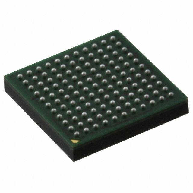


 工商网监
湘ICP备2023018690号
工商网监
湘ICP备2023018690号
