NXP Semiconductors
Data Sheet: Technical Data
Kinetis K28F MCU Sub-Family
K28P210M150SF5
Rev. 4, 03/2017
MK28FN2M0CAU15R
High performance ARM® Cortex®-M4 MCU with 2 MB Flash,
MK28FN2M0VMI15
1 MB SRAM, 2 USB Controllers (High-Speed and FullSpeed), SDRAM controller, QuadSPI interface and Power
Management Controller with Core Voltage Bypass.
K28F extends the Kinetis Micontroller portfolio with large
embedded memory, advanced external memory interfaces,
performance, and peripheral integration while maintaining a high
level of software compatibility with previous Kinetis devices:
• The extended memory resources include a total of 2 MB of
programmable flash and 1 MB of embedded SRAM which
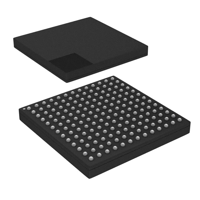
169 MAPBGA (MI)
210 WLCSP (AU)
can be used to support application needs for data logging
9 x 9 x 1.28 mm Pitch 6.9 mm x 6.9 x 0.6 mm
and rich human to machine interfaces with displays
0.65 mm
Pitch 0.4 mm
• The Power Management Controller with Core Voltage
Bypass enables the use of an external PMIC to maximize
the power efficiency of the system
• K28F enables memory expansion leveraging the SDRAM
controller and QuadSPI interface for eXecution-In-Place (XIP) from an external Serial NOR flash
• Both the USB High-Speed and Crystal-less Full-Speed Controllers integrate a PHY to reduce BOM cost
• The integrated smart peripherals such as Low-power UARTs and Timers operate in very low-power
modes to optimize battery life of the system
Performance
Human-machine interface
• Up to 150 MHz ARM Cortex-M4 based core with DSP
• Up to 120 General-purpose input/output (GPIOs)
instructions and Single Precision Floating Point unit
Analog modules
(FPU)
• Power Management Control (PMC) with Core Voltage
Memories and memory expansion
Bypass
• 2 MB dual bank program flash and 1 MB SRAM
• One 16-bit SAR ADCs, two 6-bit DAC and one 12-bit
• 8 KB I/D + 8 KB System cache
DAC
• 32-bit external bus interface (FlexBus)
• Two analog comparators (CMP) containing a 6-bit
• 32-bit SDRAM controller
DAC and programmable reference input
• Dual QuadSPI interface with eXecution-In-Place (XIP)
• 1.2 V Voltage reference
• supports SDR and DDR serial flash and octal
Timers
configurations
• One 4-ch 32-bit Periodic interrupt timer
• 32 KB Boot ROM with built-in bootloader
• Two 16-bit low-power timer PWM modules
System and Clocks
• Two 8-ch motor control/general purpose/PWM timers
• 32-ch Asynchronous DMA
• Two 2-ch quadrature decoder/general purpose timers
• Multiple low-power modes
• Real-time clock with independent 3.6 V power domain
• Memory protection unit with multi-master protection
• Programmable delay block
• 3 to 32 MHz main crystal oscillator
Operating Characteristics
• 32 kHz low power crystal oscillator
• Temperature range (ambient): -40 to 105°C (BGA)
• 48 MHz internal reference
Temperature range (ambient):-40 to 85°C (WLCSP)
• Hardware and Software Watchdogs
NXP reserves the right to change the production detail specifications as may be
required to permit improvements in the design of its products.
�Security
• Hardware random-number generator
• Memory Mapped Crypto Acceleration Unit(MMCAU):
DES, 3-DES, AES, SHA-1, SHA-256 and MD5
accelerator
• Cyclic Redundancy Check (CRC)
Target Applications
• Wearables
• Low-end graphic display system
• Cost-optimized multi-standard wireless smart home
hubs
• Home Automation devices
• Consumer accessories
• Main VDD Voltage and Flash write voltage range:1.71
V–3.6 V
• VDD_CORE: 1.17 V–1.47 V
• Independent VDDIO_E (QuadSPI):1.71 V–3.6 V
• Independent VBAT (RTC): 1.71 V–3.6 V
• I/O Voltage range (VDD): 1.71 V–3.6 V
Communication interfaces
• Two USB controllers:Crystal-less Full-/low-speed +
transceiver Host and Device; High-/Full-/low-speed +
PHY Host and Device
• Secure Digital Host Controller (SDHC)
• Two I2S modules, four I2C modules and five LowPower UART modules
• Four SPI modules (SPI3 supports more than 40
Mbps)
• 32-ch Programmable module (FlexIO) to emulate
various serial, parallel or custom interfaces
Ordering Information 1
Part Number
Embedded Memory
Package Type
Maximum number of
I\O's
Flash
SRAM
MK28FN2M0VMI15
2 MB
1 MB
169 MAPBGA
120
MK28FN2M0CAU15R
2 MB
1 MB
210 WLCSP
120
1. To confirm current availability of orderable part numbers, go to http://www.nxp.com and perform a part number search.
Device Revision Number
Device Mask Set Number
SIM_SDID[REVID]
JTAG ID Register[PRN]
2N96T
0010
0010
Related Resources
Type
Description
Resource
Fact Sheet
The Fact Sheet gives overview of the product key features and its uses.
K2x Fact Sheet
Reference
Manual
The Reference Manual contains a comprehensive description of the
structure and function (operation) of a device.
K28P210M150SF5RM1
Data Sheet
The Data Sheet includes electrical characteristics and signal
connections.
This document
Chip Errata
The chip mask set Errata provides additional or corrective information for Kinetis_K_2N96T1
a particular device mask set.
Package
drawing
Package dimensions are provided in package drawings.
• MAPBGA 169-pin:
98ASA00628D1
• WLCSP 210-pin:
98ASA01002D 1
1. To find the associated resource, go to http://www.nxp.com and perform a search using this term.
2
NXP Semiconductors
Kinetis K28F MCU Sub-Family, Rev. 4, 03/2017
�Cryptographic
accelerator
(CAU)
Trace
Port
TPIU
JTAG &
Serial Wire
SWJ-DP
ARM Cortex M4
ETM
PPB
AHB-AP
NVIC
PIT
ITM
WIC
FPU
DWT
IRC
48 MHz
OSC
DMA
Mux x2
DCD
USB/
FS/LS
USB
Vreg
MUX
256 KByte
MCG
PLL
HS DCD
FPB
USB
HS/FS/ LS
DSP
System
ICODE
DCODE
256 KByte
RTC
OSC
eDMA
eSDHC
Cache
SRAM
8 Kbyte
M0
8 Kbyte
M1
M5
M3
Crossbar Switch (XBS)
M2
M4
S2
System Memory Protection Unit (MPU)
S1
IRC
4 MHz
FLL
PLL
S5
QSPI
S6
S0
BOOT
ROM
Flash
Controller
S4
SDRAMC
S3
BME2
AHB to IPS 0
FlexBus
RGPIO
AHB to IPS 1
x128
512 KByte
OCRAM
4 KByte
EERAM
Flash
6-bit DAC
& CMP x2
SPI
x4
FlexIO
PDB
PIT
16-bit ADC
I2C
x4
LPUART
x5
FlexTimer
x4
TRNG
CMT
TPM
x2
CRC
RTC
Low-power
timer x2
PMC
with bypass
512 KByte 512 KByte
512 KByte 512 KByte
Vref
I2S
x2
12-bit DAC
Figure 1. K28F Block Diagram
Kinetis K28F MCU Sub-Family, Rev. 4, 03/2017
3
NXP Semiconductors
�Table of Contents
1 Ratings.................................................................................... 5
1.1 Thermal handling ratings................................................. 5
1.2 Moisture handling ratings................................................ 5
1.3 ESD handling ratings....................................................... 5
1.4 Voltage and current maximum ratings............................. 5
1.4.1 Recommended Power-On-Reset (POR)
Sequencing .........................................................6
2 General................................................................................... 7
2.1 AC electrical characteristics.............................................7
2.2 Nonswitching electrical specifications..............................7
2.2.1 Voltage and current operating requirements....... 7
2.2.2 HVD, LVD and POR operating requirements...... 8
2.2.3
2.2.4
2.2.5
2.2.6
Voltage and current operating behaviors.............9
Power mode transition operating behaviors........ 11
Power consumption operating behaviors............ 12
Electromagnetic Compatibility (EMC)
specifications....................................................... 23
2.2.7 Designing with radiated emissions in mind..........23
2.2.8 Capacitance attributes.........................................23
2.3 Switching specifications...................................................23
2.3.1 Device clock specifications..................................23
2.3.2 General switching specifications......................... 24
2.4 Thermal specifications..................................................... 25
2.4.1 Thermal operating requirements......................... 25
2.4.2 Thermal attributes................................................26
3 Peripheral operating requirements and behaviors.................. 27
3.1 Core modules.................................................................. 27
3.1.1 Debug trace timing specifications........................27
3.1.2 JTAG electricals.................................................. 28
3.2 Clock modules................................................................. 31
3.2.1 MCG specifications..............................................31
3.2.2 IRC48M specifications.........................................34
3.2.3 Oscillator electrical specifications........................35
3.2.4 32 kHz oscillator electrical characteristics........... 37
3.3 Memories and memory interfaces................................... 37
3.3.1 QuadSPI AC specifications................................. 37
3.3.2 Flash electrical specifications.............................. 43
3.3.3 Flexbus switching specifications..........................45
3.3.4 SDRAM controller specifications......................... 47
3.4 Analog............................................................................. 50
4
NXP Semiconductors
4
5
6
7
8
3.4.1 ADC electrical specifications............................... 50
3.4.2 CMP and 6-bit DAC electrical specifications....... 54
3.4.3 12-bit DAC electrical characteristics....................56
3.4.4 Voltage reference electrical specifications.......... 59
3.5 Timers..............................................................................60
3.6 Communication interfaces............................................... 60
3.6.1 USB Voltage Regulator electrical specifications..61
3.6.2 USB Full Speed Transceiver and High Speed
PHY specifications...............................................62
3.6.3 USB DCD electrical specifications.......................62
3.6.4 DSPI switching specifications (limited voltage
range).................................................................. 63
3.6.5 DSPI switching specifications (full voltage
range).................................................................. 66
3.6.6 Inter-Integrated Circuit Interface (I2C) timing...... 68
3.6.7 LPUART switching specifications........................ 70
3.6.8 SDHC specifications............................................70
3.6.9 I2S switching specifications.................................72
Dimensions............................................................................. 78
4.1 Obtaining package dimensions....................................... 78
Pinout...................................................................................... 78
5.1 K28F Signal Multiplexing and Pin Assignments.............. 78
5.2 Recommended connection for unused analog and
digital pins........................................................................79
5.3 K28F Pinouts................................................................... 80
Ordering parts......................................................................... 80
6.1 Determining valid orderable parts....................................80
Part identification.....................................................................81
7.1 Description.......................................................................81
7.2 Format............................................................................. 81
7.3 Fields............................................................................... 81
7.4 Example...........................................................................82
Terminology and guidelines.................................................... 82
8.1
8.2
8.3
8.4
Definitions........................................................................ 82
Examples......................................................................... 83
Typical-value conditions.................................................. 83
Relationship between ratings and operating
requirements....................................................................84
8.5 Guidelines for ratings and operating requirements..........84
9 Revision History...................................................................... 85
Kinetis K28F MCU Sub-Family, Rev. 4, 03/2017
�Ratings
1 Ratings
1.1 Thermal handling ratings
Symbol
Description
Min.
Max.
Unit
Notes
TSTG
Storage temperature
–55
150
°C
1
TSDR
Solder temperature, lead-free
—
260
°C
2
1. Determined according to JEDEC Standard JESD22-A103, High Temperature Storage Life.
2. Determined according to IPC/JEDEC Standard J-STD-020, Moisture/Reflow Sensitivity Classification for Nonhermetic
Solid State Surface Mount Devices.
1.2 Moisture handling ratings
Symbol
Description
Min.
Max.
Unit
Notes
MSL
Moisture sensitivity level (for V-temp variant)
—
3
—
1
MSL
Moisture sensitivity level (for C-temp variant)
—
1
—
1
1. Determined according to IPC/JEDEC Standard J-STD-020, Moisture/Reflow Sensitivity Classification for Nonhermetic
Solid State Surface Mount Devices.
1.3 ESD handling ratings
Symbol
Description
Min.
Max.
Unit
Notes
VHBM
Electrostatic discharge voltage, human body model
-2000
+2000
V
1
VCDM
Electrostatic discharge voltage, charged-device
model
-500
+500
V
2
Latch-up current at ambient temperature of 105°C
-100
+100
mA
3
ILAT
1. Determined according to JEDEC Standard JESD22-A114, Electrostatic Discharge (ESD) Sensitivity Testing Human
Body Model (HBM).
2. Determined according to JEDEC Standard JESD22-C101, Field-Induced Charged-Device Model Test Method for
Electrostatic-Discharge-Withstand Thresholds of Microelectronic Components.
3. Determined according to JEDEC Standard JESD78, IC Latch-Up Test.
1.4 Voltage and current maximum ratings
Kinetis K28F MCU Sub-Family, Rev. 4, 03/2017
5
NXP Semiconductors
�Ratings
Symbol
Description
Min.
Max.
Unit
Internal digital logic supply voltage
– 0.3
1.47
V
VDD
Digital supply voltage for Ports A, B,C,D
–0.3
3.8
V
VDDA
Analog supply voltage
– 0.3
3.8
V
–0.3
3.8
V
1
VDD_CORE
VDDIO_E
VBAT
VDDIO_E is an independent voltage supply for PORTE
RTC supply voltage
2
–0.3
3.8
V
—
300
mA
Maximum current single pin limit (digital output pins)
–25
25
mA
USB regulator input
–0.3
6.0
V
VUSB0_Dx
USB0_DP and USB_DM input voltage
–0.3
3.63
V
VUSB1_DPx
USB1_DP and USB1_DM input voltage
–0.3
3.63
V
IDD
Digital supply current
ID
VREGIN
1. VDD_CORE must not exceed VDD on power up or power down
2. VDDIO_E is independent of the VDD domain and can operate at a voltage independent of VDD.
1.4.1 Recommended Power-On-Reset (POR) Sequencing
• VDD/VDDIO_E and VDD_CORE
Figure 2. VDD_CORE/ VDD Powering sequence
6
NXP Semiconductors
Kinetis K28F MCU Sub-Family, Rev. 4, 03/2017
�General
2 General
2.1 AC electrical characteristics
Unless otherwise specified, propagation delays are measured from the 50% to the 50%
point, and rise and fall times are measured at the 20% and 80% points, as shown in the
following figure.
Input Signal
High
Low
VIH
80%
50%
20%
Midpoint1
VIL
Fall Time
Rise Time
The midpoint is VIL + (VIH - VIL) / 2
Figure 3. Input signal measurement reference
All digital I/O switching characteristics assume:
1. output pins
• have CL=15 pF loads,
• are slew rate disabled, and
• are normal drive strength
2. input pins
• have their passive filter disabled (PORTx_PCRn[PFE]=0)
2.2 Nonswitching electrical specifications
2.2.1 Voltage and current operating requirements
Table 1. Voltage and current operating requirements
Symbol
Description
Min.
Max.
Unit
VDD_CORE
(RUN)
Core and digital logic supply voltage for RUN mode
1.17
1.32
V
VDD_CORE
(HSRUN)
Core and digital logic supply voltage for HSRUN
1.33
1.47
V
Notes
Table continues on the next page...
Kinetis K28F MCU Sub-Family, Rev. 4, 03/2017
7
NXP Semiconductors
�General
Table 1. Voltage and current operating requirements (continued)
Symbol
Description
Min.
Max.
Unit
Digital supply voltage for Ports A, B, C,D
1.71
3.6
V
Digital Supply voltage for Port E
1.71
3.6
V
Analog supply voltage
1.71
3.6
V
VDD – VDDA VDD-to-VDDA differential voltage
–0.1
0.1
V
VSS – VSSA VSS-to-VSSA differential voltage
–0.1
0.1
V
1.71
3.6
V
0.7 × VDD
—
V
0.75 × VDD
—
V
—
0.35 × VDD
V
—
0.3 × VDD
V
0.7 ×
VDDIO_E
—
V
—
V
0.35 ×
VDDIO_E
V
VDD
VDDIO_E
VDDA
VBAT
VIH
RTC battery supply voltage
Input high voltage
• 2.7 V ≤ VDD ≤ 3.6 V
• 1.7 V ≤ VDD ≤ 2.7 V
VIL
Notes
Input low voltage
• 2.7 V ≤ VDD ≤ 3.6 V
• 1.7 V ≤ VDD ≤ 2.7 V
VIH_E
Input high voltage
• 2.7 V ≤ VDDIO_E ≤ 3.6 V
• 1.7 V ≤ VDDIO_E ≤ 2.7 V
VIL_E
Input low voltage
• 2.7 V ≤ VDDIO_E ≤ 3.6 V
0.75 ×
VDDIO_E
—
—
V
0.3 ×
VDDIO_E
• 1.7 V ≤ VDDIO_E ≤ 2.7 V
VHYS
Input hysteresis
0.06 × VDD
—
V
VHYS_E
Input hysteresis
0.06 ×
VDDIO_E
—
V
-5
—
mA
-25
—
mA
VDD
VDD
V
1.14
1.47
V
VPOR_VBAT
—
V
IICIO
I/O pin negative DC injection current — single pin
• VIN < VSS-0.3V
IICcont
Contiguous pin DC injection current —regional limit,
includes sum of negative injection currents or sum of
positive injection currents of 16 contiguous pins
• Negative current injection
VODPU
Pseudo Open drain pullup voltage level
VRAM
VDD_CORE voltage required to retain RAM
VRFVBAT
VBAT voltage required to retain the VBAT register file
1
2
1. All I/O pins are internally clamped to VSS through an ESD protection diode. There is no diode connection to VDD or
VDDIO_E. If VIN is less than -0.3V, a current limiting resistor is required. The negative DC injection current limiting resistor
is calculated as R=(-0.3-VIN)/|IICIO|. The actual resistor value should be an order of magnitude higher to tolerate transient
voltages.
2. Open drain outputs must be pulled to VDD.
8
NXP Semiconductors
Kinetis K28F MCU Sub-Family, Rev. 4, 03/2017
�General
2.2.2 HVD, LVD and POR operating requirements
Table 2. VDD supply HVD, LVD and POR operating requirements
Symbol
Description
Min.
Typ.
Max.
Unit
VHVDH
High Voltage Detect (High Trip Point)
—
3.72
—
V
VHVDL
High Voltage Detect (Low Trip Point)
—
3.46
—
V
VPOR
Falling VDD POR detect voltage
0.8
1.1
1.5
V
VLVDH
Falling low-voltage detect threshold — high
range (LVDV=01)
2.48
2.56
2.64
V
2.62
2.70
2.78
V
2.72
2.80
2.88
V
2.82
2.90
2.98
V
2.92
3.00
3.08
V
—
60
—
mV
1.54
1.60
1.66
V
1.74
1.80
1.86
V
1.84
1.90
1.96
V
1.94
2.00
2.06
V
2.04
2.10
2.16
V
—
40
—
mV
VLVW1H
VLVW2H
VLVW3H
VLVW4H
Low-voltage warning thresholds — high range
• Level 1 falling (LVWV=00)
• Level 2 falling (LVWV=01)
• Level 3 falling (LVWV=10)
Low-voltage inhibit reset/recover hysteresis —
high range
VLVDL
Falling low-voltage detect threshold — low
range (LVDV=00)
VLVW2L
VLVW3L
VLVW4L
VHYSL
1
• Level 4 falling (LVWV=11)
VHYSH
VLVW1L
Notes
Low-voltage warning thresholds — low range
• Level 1 falling (LVWV=00)
• Level 2 falling (LVWV=01)
• Level 3 falling (LVWV=10)
1
• Level 4 falling (LVWV=11)
Low-voltage inhibit reset/recover hysteresis —
low range
VBG
Bandgap voltage reference
0.97
1.00
1.03
V
tLPO
Internal low power oscillator period — factory
trimmed
900
1000
1100
μs
1. Rising threshold is the sum of falling threshold and hysteresis voltage
NOTE
There is no LVD circuit for VDDIO_E and VDD_CORE domain.
Table 3. VBAT power operating requirements
Symbol
Description
VPOR_VBAT Falling VBAT supply POR detect voltage
Kinetis K28F MCU Sub-Family, Rev. 4, 03/2017
Min.
Typ.
Max.
Unit
0.8
1.1
1.5
V
Notes
9
NXP Semiconductors
�General
2.2.3 Voltage and current operating behaviors
Table 4. Voltage and current operating behaviors
Symbol
VOH
Description
Typ.1
Min.
Max.
Unit
Output high voltage — normal drive strength
IO Group 1
• 2.7 V ≤ VBAT ≤ 3.6 V, IOH = -5 mA
• 1.71 V ≤ VBAT ≤ 2.7 V, IOH = -2.5 mA
IO Groups 2 and 3
• 2.7 V ≤ VDD ≤ 3.6 V, IOH = -10 mA
• 1.71 V ≤ VDD ≤ 2.7 V, IOH = -5 mA
IO Group 4
• 2.7 V ≤ VDDIO_E ≤ 3.6 V, IOH = -5 mA
• 1.71 V ≤ VDDIO_E ≤ 2.7 V, IOH = -2.5 mA
2, 3
VBAT – 0.5
—
—
V
VBAT – 0.5
—
—
V
—
—
V
—
—
V
—
—
V
—
—
V
VDD – 0.5
VDD – 0.5
VDDIO_E – 0.5
VDDIO_E – 0.5
Output high voltage — High drive strength
IO Group 3
• 2.7 V ≤ VDD ≤ 3.6 V, IOH = -20 mA
• 1.71 V ≤ VDD ≤ 2.7 V, IOH = -10 mA
IO Group 4
• 2.7 V ≤ VDDIO_E ≤ 3.6 V, IOH = -15 mA
• 1.71 V ≤ VDDIO_E ≤ 2.7 V, IOH = -7.5 mA
IOHT
Output high current total for all ports
VOL
Output low voltage — normal drive strength
Notes
2
VDD – 0.5
—
—
V
VDD – 0.5
—
—
V
VDDIO_E – 0.5
—
—
V
VDDIO_E – 0.5
—
—
V
—
—
100
mA
2, 4, 5
IO Group 1
• 2.7 V ≤ VBAT ≤ 3.6 V, IOL = -5 mA
• 1.71 V ≤ VBAT ≤ 2.7 V, IOL = -2.5 mA
IO Groups 2 and 3
• 2.7 V ≤ VDD ≤ 3.6 V, IOL = -10 mA
• 1.71 V ≤ VDD ≤ 2.7 V, IOL = -5 mA
IO Group 4
• 2.7 V ≤ VDDIO_E ≤ 3.6 V, IOL = -5 mA
• 1.71 V ≤ VDDIO_E ≤ 2.7 V, IOL = -2.5 mA
—
—
0.5
V
—
—
0.5
V
—
—
0.5
V
—
—
0.5
V
—
—
0.5
V
—
—
0.5
V
Output low voltage — High drive strength
2, 4
IO Group 3
• 2.7 V ≤ VDD ≤ 3.6 V, IOL = -20 mA
• 1.71 V ≤ VDD ≤ 2.7 V, IOL = -10 mA
IO Group 4
• 2.7 V ≤ VDDIO_E ≤ 3.6 V, IOL = -15 mA
• 1.71 V ≤ VDDIO_E ≤ 2.7 V, IOL = -7.5 mA
IOLT
IIN
Output low current total for all ports
—
—
0.5
V
—
—
0.5
V
—
—
0.5
V
—
—
0.5
V
—
—
100
mA
Input leakage current
6, 7, 8
Table continues on the next page...
10
NXP Semiconductors
Kinetis K28F MCU Sub-Family, Rev. 4, 03/2017
�General
Table 4. Voltage and current operating behaviors (continued)
Symbol
Description
VDD domain pins
• VSS ≤ VIN ≤ VDD
PORTE pins
• VSS ≤ VIN ≤ VDDIO_E
Min.
Typ.1
Max.
Unit
—
0.002
0.5
µA
—
0.002
0.5
µA
—
0.002
0.5
µA
Notes
VBAT domain pins
• VSS ≤ VIN ≤ VBAT
RPU
Internal pullup resistors(except RTC_WAKEUP
pins)
20
—
50
kΩ
9
RPD
Internal pulldown resistors (except RTC_WAKEUP
pins)
20
—
50
kΩ
10
1. Typical values characterized at 25°C and VDD = 3.6V unless otherwise noted.
2. IO Group 1 includes VBAT domain pins: RTC_WAKEUP_b. IO Group 2 includes VDD domain pins: PORTA, PORTB,
PORTC, and PORTD, except PTA4. IO Group 3 includes VDD domain pins: PTB0, PTB1, PTC3, PTC4, PTD4, PTD5,
PTD6, and PTD7. IO Group 4 includes VDDIO_E domain pins: PORTE.
3. PTA4 has lower drive strength: IOH = -5 mA for high VDD range; IOH = -2.5 mA for low VDD range.
4. Open drain outputs must be pulled to VDD.
5. PTA4 has lower drive strength: IOL = 5mA for high VDD range; IOL = 2.5mA for low VDD range.
6. VDD domain pins include ADC, CMP, and RESET_b inputs. Measured at VDD = 3.6V.
7. PORTE analog input voltages cannot exceed VDDIO_E supply when VDD ≥ VDDIO_E. PORTE analog input voltages
cannot exceed VDD supply when VDD ˂ VDDIO_E.
8. VBAT domain pins include EXTAL32, XTAL32, and RTC_WAKEUP_b pins.
9. Measured at minimum supply voltage and VIN = VSS
10. Measured at minimum supply voltage and VIN = VDD
2.2.4 Power mode transition operating behaviors
All specifications except tPOR, and VLLSx –> RUN recovery times in the following
table assume this clock configuration:
•
•
•
•
•
CPU and system clocks = 100 MHz
Bus clock = 50 MHz
FlexBus clock = 50 MHz
Flash clock = 25 MHz
MCG mode=FEI
Table 5. Power mode transition operating behaviors
Symbol
tPOR
Description
After a POR event, amount of time from the point
VDD reaches 1.71 V and VDD_CORE reaches 1.17
V to execution of the first instruction across the
operating temperature range of the chip.
Min.
Max.
Unit
—
1200
µs
Notes
Table continues on the next page...
Kinetis K28F MCU Sub-Family, Rev. 4, 03/2017
11
NXP Semiconductors
�General
Table 5. Power mode transition operating behaviors (continued)
Symbol
Description
• VLLS2 –> RUN
• VLLS3 –> RUN
• LLS2 –> RUN
• LLS3 –> RUN
• VLPS –> RUN
• STOP –> RUN
Min.
Max.
Unit
—
103
µs
—
103
µs
—
6.3
µs
—
6.3
µs
—
5.4
µs
—
5.4
µs
Notes
2.2.5 Power consumption operating behaviors
Figure 4. Power Supplies of K28F
The K28F device has several power supplies and the total current consumption of the
device is the accumulative result of each individual power supplies’ current
consumption, dependent on the power mode of operation. (RUN, HSRUN, VLPR, Stop,
VLLS3 etc.).
IDD_MCU_total = IDDC + IDD + IDDIO_E + IDD_VBAT + IDDA + IDD_USB
When calculating the total MCU current consumption considerations to external loads
on the following should be made:
• On top of the device’s IDD current consumption, external loads applied to Ports
A,B,C and D need to be considered
12
NXP Semiconductors
Kinetis K28F MCU Sub-Family, Rev. 4, 03/2017
�General
• IDDIO_E current consumption is significantly dependent on external loads
applied to Port E pins, and the internal current consumption in the device is
negligible compared to IDD.
• The USB_VREG provides a 3.3 V output which can drive loads of upto 150 mA
need to be considered.
The maximum values stated in the following table represent characterized results
equivalent to the mean plus three times the standard deviation (mean + 3 sigma).
Table 6 details the IDDC values observed through the VDD_CORE supply and Table
7 details the IDD values observed through the VDD supply.
Table 6. Power consumption operating behaviors (through VDD_CORE)
Symbol
IDDA
IDDC_RUN
Description
Analog supply current
Run mode current — all peripheral clocks disabled,
code of while(1) loop executing from internal flash at
1.2 V
• @ 25°C
• @ 70°C
• @ 85°C
• @ 105°C
IDDC_RUN
Run mode current — all peripheral clocks enabled,
code of while(1) loop executing from internal flash at
1.2 V
Max.
Unit
Notes
—
—
See note
mA
1
2
mA
—
31.0
35.1
—
37.9
51.6
—
42.7
63.6
—
51.9
85.7
2
mA
41.6
47.1
—
48.0
65.5
• @ 85°C
—
52.6
78.4
• @ 105°C
—
61.1
100.9
• @ 70°C
Run mode current in compute operation - 120 MHz
core / 24 MHz flash / bus clock disabled, code of
while(1) loop executing from internal flash at 1.2 V
• @ 25°C
• @ 70°C
• @ 85°C
• @ 105°C
IDDC_HSRUN
Typ.
—
• @ 25°C
IDDC_RUNCO
Min.
3
mA
—
28.5
32.4
—
35.5
48.4
—
40.3
60.1
—
49.5
81.6
High-speed Run mode current — all peripheral
clocks disabled, code of while(1) loop executing from
internal flash at 1.4 V
• @ 25°C
• @ 70°C
4
mA
—
42.6
49.6
—
53.5
74.9
Table continues on the next page...
Kinetis K28F MCU Sub-Family, Rev. 4, 03/2017
13
NXP Semiconductors
�General
Table 6. Power consumption operating behaviors (through VDD_CORE) (continued)
Symbol
Description
• @ 85°C
• @ 105°C
IDDC_HSRUN
High-speed Run mode current — all peripheral
clocks enabled, code of while(1) loop executing from
internal flash at 1.4 V
• @ 25°C
• @ 70°C
• @ 85°C
• @ 105°C
IDDC_HSRUNCO High-speed Run mode current in compute operation
– 150 MHz core/ 25 MHz flash / bus clock disabled,
code of while(1) loop executing from internal flash at
1.4 V
• @ 25°C
• @ 70°C
• @ 85°C
• @ 105°C
IDDC_WAIT
• @ 70°C
• @ 85°C
• @ 105°C
Max.
59.7
91.3
—
71.7
121.0
Unit
• @ 70°C
• @ 85°C
• @ 105°C
Very-low-power run mode current at 1.2 V — all
peripheral clocks disabled, code of while(1) loop
executing out of internal flash
• @ 25°C
• @ 70°C
• @ 85°C
• @ 105°C
Notes
4
—
54.3
63.3
—
65.7
91.9
—
71.5
109.8
—
82.6
139.0
mA
3
—
40.5
47.2
—
50.7
70.9
—
57.1
87.2
—
68.7
115.7
mA
2
—
15.6
17.7
—
23.2
31.6
—
28.3
42.2
—
38.1
62.8
mA
Wait mode reduced frequency current at 1.2 V— all
peripheral clocks disabled
• @ 25°C
IDDC_VLPR
Typ.
—
Wait mode high frequency current at 1.2 V— all
peripheral clocks disabled
• @ 25°C
IDDC_WAIT
Min.
5
—
7.0
7.9
—
15.0
20.4
—
20.3
30.3
—
30.5
50.4
mA
6
mA
—
1.2
3.9
—
2.6
7.1
—
3.8
9.7
—
6.2
15.0
Table continues on the next page...
14
NXP Semiconductors
Kinetis K28F MCU Sub-Family, Rev. 4, 03/2017
�General
Table 6. Power consumption operating behaviors (through VDD_CORE) (continued)
Symbol
IDDC_VLPR
Description
Min.
Very-low-power run mode current at 1.2 V — all
peripheral clocks enabled, code of while(1) loop
executing out of internal flash
• @ 25°C
• @ 70°C
• @ 85°C
• @ 105°C
IDDC_VLPRCO Very-low-power run mode current in compute
operation - 4 MHz core / 1 MHz flash / bus clock
disabled, code of while(1) loop executing from
internal flash at 1.2 V
• @ 25°C
• @ 70°C
• @ 85°C
• @ 105°C
IDDC_PSTOP2
Stop mode current with partial stop 2 clocking option
- core and system disabled / 10.5 MHz bus at 1.2 V
• @ 25°C
• @ 70°C
• @ 85°C
• @ 105°C
IDDC_VLPW
Very-low-power wait mode current at 1.2 V — all
peripheral clocks disabled
• @ 25°C
• @ 85°C
IDDC_VLPW
1.7
5.5
—
3.1
8.5
—
4.3
11.0
—
6.7
16.2
Very-low-power wait mode current at 1.2 V— all
peripheral clocks enabled
• @ 25°C
Unit
Notes
mA
7
—
1.1
3.6
—
2.5
6.9
—
3.7
9.5
—
6.1
14.8
mA
3
—
4.4
14.2
—
9.8
26.5
—
13.0
33.4
—
15.7
37.9
mA
6
—
—
0.759
2.5
2.2
5.9
3.3
8.6
5.8
14.0
mA
6
—
1.2
4.0
• @ 70°C
—
2.7
7.2
• @ 85°C
—
3.8
9.8
—
6.3
15.1
• @ 25°C
—
0.749
1.9
• @ 70°C
—
3.4
7.5
—
5.4
11.3
—
9.1
18.7
• @ 105°C
IDDC_STOP
—
—
• @ 105°C
Max.
6
—
• @ 70°C
Typ.
mA
Stop mode current at 1.2 V
• @ 85°C
mA
• @ 105°C
Table continues on the next page...
Kinetis K28F MCU Sub-Family, Rev. 4, 03/2017
15
NXP Semiconductors
�General
Table 6. Power consumption operating behaviors (through VDD_CORE) (continued)
Symbol
IDDC_VLPS
Description
Min.
Typ.
Max.
Unit
• @ 25°C
—
0.452
1.2
mA
• @ 70°C
—
2.2
4.9
—
3.4
7.4
—
5.8
12.4
—
15.6
30.3
—
129.0
189.5
—
244.9
347.8
—
535.0
737.3
Very-low-power stop mode current at 1.2 V
• @ 85°C
• @ 105°C
IDDC_LLS3
Notes
Low leakage stop mode current at 1.2 V
• @ 25°C
μA
• @ 70°C
• @ 85°C
• @ 105°C
IDDC_LLS2
Low leakage stop mode current at 1.2 V
• @ 25°C
—
4.3
8.7
• @ 70°C
—
33.8
57.3
• @ 85°C
—
62.8
104.0
—
135.6
205.8
• @ 25°C
—
13.5
26.0
• @ 70°C
—
112.1
159.7
212.5
294.7
460.2
621.6
• @ 105°C
IDDC_VLLS3
8
Very low-leakage stop mode 3 current at 1.2 V
• @ 85°C
—
• @ 105°C
—
IDDC_VLLS2
μA
Very low-leakage stop mode 2 current at 1.2 V
8
• @ 25°C
—
0.552
0.9
• @ 70°C
—
6.1
8.2
—
10.5
14.2
—
24.7
32.3
—
0.266
0.319
—
0.595
0.750
—
0.933
1.3
—
2.2
2.8
• @ 85°C
• @ 105°C
IDD_VBAT
μA
Average current with RTC and 32 kHz disabled @
3.0 V
• @ 25°C
μA
μA
• @ 70°C
• @ 85°C
• @ 105°C
IDD_VBAT
Average current when CPU is not accessing RTC
registers @ 1.8 V
16
NXP Semiconductors
9
μA
Kinetis K28F MCU Sub-Family, Rev. 4, 03/2017
�General
Table 6. Power consumption operating behaviors (through VDD_CORE)
Symbol
Description
Min.
Typ.
Max.
• @ 25°C
—
0.454
0.546
• @ 70°C
—
0.724
0.897
—
1.1
1.4
—
2.0
2.6
• @ 85°C
Unit
Notes
• @ 105°C
1. The analog supply current is the sum of the active or disabled current for each of the analog modules on the device.
See each module's specification for its supply current.
2. 120 MHz core and system clock, 60 MHz bus and FlexBus clock, and 24 MHz flash clock. MCG configured for PEE
mode.
3. MCG configured for PEE mode.
4. 150 MHz core and system clock, 50 MHz bus and FlexBus clock, and 25 MHz flash clock. MCG configured for PEE
mode.
5. 25 MHz core and system clock, 25 MHz bus and FlexBus clock, and 25 MHz flash clock. MCG configured for FEI
mode
6. 4 MHz core, system, FlexBus, and bus clock and 1 MHz flash clock. MCG configured for BLPE mode. Code executing
from flash.
7. MCG configured for BLPE mode.
8. By default, this mode only has 32 K of SRAM enabled.
9. Includes 32 kHz oscillator current and RTC operation.
Table 7. Power consumption operating behaviors (through VDD)
Symbol
Description
Min.
IDD_RUN
Run mode current — all peripheral clocks disabled,
code of while(1) loop executing from internal flash @
3.0 V
• @ 25°C
• @ 70°C
• @ 85°C
• @ 105°C
IDD_RUN
Run mode current — all peripheral clocks enabled,
code of while(1) loop executing from internal flash @
3.0 V
• @ 25°C
• @ 70°C
• @ 85°C
• @ 105°C
IDD_RUNCO
Typ.
Max.
• @ 70°C
Notes
1
—
2.0
2.1
—
2.0
2.1
—
2.0
2.1
—
2.0
2.1
mA
1
—
2.0
2.1
—
2.0
2.1
—
2.0
2.1
—
2.0
mA
2.1
Run mode current in compute operation - 120 MHz
core / 24 MHz flash / bus clock disabled, code of
while(1) loop executing from internal flash at 3.0 V
• @ 25°C
Unit
2
mA
—
1.5
1.6
—
1.5
1.7
Table continues on the next page...
Kinetis K28F MCU Sub-Family, Rev. 4, 03/2017
17
NXP Semiconductors
�General
Table 7. Power consumption operating behaviors (through VDD) (continued)
Symbol
Description
• @ 85°C
Min.
Typ.
Max.
—
1.6
1.7
—
1.6
1.7
Unit
Notes
• @ 105°C
IDD_HSRUN
Run mode current — all peripheral clocks disabled,
code of while(1) loop executing from internal flash @
3.0 V
• @ 25°C
• @ 70°C
• @ 85°C
• @ 105°C
IDD_HSRUN
Run mode current — all peripheral clocks enabled,
code of while(1) loop executing from internal flash @
3.0 V
• @ 25°C
• @ 70°C
• @ 85°C
• @ 105°C
3
—
2.0
2.1
—
2.0
2.1
—
2.0
2.1
—
2.0
2.1
3
—
2.0
2.1
—
2.0
2.1
—
2.0
2.1
—
2.0
2.1
IDD_HSRUNCO HSRun mode current in compute operation – 150 MHz
core/ 25 MHz flash / bus clock disabled, code of
while(1) loop executing from internal flash at 3.0 V
• @ 25°C
• @ 70°C
mA
mA
2
mA
—
2.0
2.1
—
2.0
2.1
—
2.0
2.1
—
2.0
2.1
• @ 85°C
• @ 105°C
IDD_WAIT
Wait mode high frequency current at 3.0 V — all
peripheral clocks disabled
• @ 25°C
• @ 70°C
• @ 85°C
• @ 105°C
IDD_WAIT
1
—
2.0
2.1
—
2.0
2.1
—
2.0
2.1
—
2.0
2.1
mA
Wait mode reduced frequency current at 3.0 V — all
peripheral clocks disabled
• @ 25°C
• @ 70°C
• @ 85°C
• @ 105°C
4
—
2.0
2.1
—
2.0
2.1
—
2.0
2.1
—
2.0
2.1
mA
Table continues on the next page...
18
NXP Semiconductors
Kinetis K28F MCU Sub-Family, Rev. 4, 03/2017
�General
Table 7. Power consumption operating behaviors (through VDD) (continued)
Symbol
Description
Min.
IDD_VLPR
Very-low-power run mode current at 3.0 V — all
peripheral clocks disabled
• @ 25°C
• @ 70°C
• @ 85°C
• @ 105°C
IDD_VLPR
• @ 70°C
• @ 85°C
• @ 105°C
IDD_VLPRCO Very-low-power run mode current in compute
operation - 4 MHz core / 0.8 MHz flash / bus clock
disabled, while(1) code executing from internal flash at
3.0 V
• @ 25°C
Unit
—
24.9
48.0
—
31.2
70.1
—
39.6
84.5
—
63.9
157.5
µA
5
—
25.2
48.6
—
31.5
70.6
—
40.0
85.0
—
64.3
158.4
16.0
• @ 70°C
—
14.4
32.3
• @ 85°C
—
22.7
48.5
—
47.0
115.8
• @ 70°C
• @ 85°C
—
1.8
3.5
—
1.8
4.1
1.9
3.9
1.9
4.6
—
Very-low-power wait mode current at 3.0 V — all
peripheral clocks disabled
• @ 25°C
• @ 70°C
• @ 85°C
• @ 105°C
Very-low-power wait mode current at 3.0 V — all
peripheral clocks enabled
• @ 25°C
• @ 70°C
µA
2
—
• @ 105°C
µA
6
8.3
IDD_PSTOP2 Stop mode current with partial stop 2 clocking option core and system disabled / 10.5 MHz bus at 3.0 V
• @ 25°C
Notes
5
—
• @ 105°C
IDD_VLPW
Max.
Very-low-power run mode current at 3.0 V — all
peripheral clocks enabled
• @ 25°C
IDD_VLPW
Typ.
mA
5
—
24.9
47.8
—
31.0
69.5
—
39.2
83.6
—
63.7
157.0
µA
5
—
25.0
48.1
—
31.2
70.0
µA
Table continues on the next page...
Kinetis K28F MCU Sub-Family, Rev. 4, 03/2017
19
NXP Semiconductors
�General
Table 7. Power consumption operating behaviors (through VDD) (continued)
Symbol
Description
• @ 85°C
• @ 105°C
IDD_STOP
Min.
Typ.
Max.
—
39.6
84.3
—
63.9
157.5
—
159.3
279.3
—
173.8
341.8
—
181.4
358.4
—
251.2
735.0
—
3.1
5.6
—
8.5
12.0
—
15.2
19.4
—
36.9
43.9
—
2.9
4.7
—
7.2
9.2
—
13.2
16.1
—
33.4
39.4
Unit
Notes
Stop mode current at 3.0 V
• @ 25°C
• @ 70°C
µA
• @ 85°C
• @ 105°C
IDD_VLPS
Very-low-power stop mode current at 3.0 V
• @ 25°C
• @ 70°C
μA
• @ 85°C
• @ 105°C
IDD_LLS3
Low leakage stop mode current at 3.0 V
• @ 25°C
• @ 70°C
μA
• @ 85°C
• @ 105°C
IDD_LLS2
IDD_VLLS3
Low leakage stop mode current at 3.0 V
7
• @ 25°C
—
2.9
4.7
• @ 70°C
—
7.2
9.2
• @ 85°C
—
13.2
16.1
• @ 105°C
—
33.4
39.4
—
2.2
3.4
—
4.7
6.4
—
8.1
10.6
—
18.8
23.8
μA
Very low-leakage stop mode 3 current at 3.0 V
• @ 25°C
• @ 70°C
μA
• @ 85°C
• @ 105°C
IDD_VLLS2
Very low-leakage stop mode 2 current at 3.0 V
• @ 25°C
7
—
2.2
3.3
—
4.5
6.1
μA
• @ 70°C
20
NXP Semiconductors
Kinetis K28F MCU Sub-Family, Rev. 4, 03/2017
�General
Table 7. Power consumption operating behaviors (through VDD)
Symbol
Description
• @ 85°C
• @ 105°C
Min.
Typ.
Max.
—
7.7
10.0
—
17.5
22.0
Unit
Notes
1. 120 MHz core and system clock, 60 MHz bus and FlexBus clock, and 24 MHz flash clock. MCG configured for PEE
mode.
2. MCG configured for PEE mode.
3. 150 MHz core and system clock, 50 MHz bus and FlexBus clock, and 25 MHz flash clock. MCG configured for PEE
mode.
4. 25 MHz core and system clock, 25 MHz bus and FlexBus clock, and 25 MHz flash clock. MCG configured for FEI
mode.
5. 4 MHz core, system, FlexBus, and bus clock and 1 MHz flash clock. MCG configured for BLPE mode. Code executing
from flash.
6. MCG configured for BLPE mode.
7. By default, this mode has only 32K of SRAM enabled.
Below table list the current consumption adders for different SRAM configurations
from the LLS2/VLLS2 (TYP) IDD values using a 32 KB SRAM retention referenced
in Table 6.
Table 8. LLS2/VLLS2 additional Typical IDDC current consumption Adders
RAM array retained
LLS2
VLLS2
@ 25°C
@ 85°C
@ 105°C
Unit
RAM2: 32 KB
0.5
10.8
21.3
µA
RAM3: 32 KB
0.5
11.0
21.5
µA
RAM4: 32 KB
0.4
10.7
21.0
µA
RAM5: 128 KB
1.4
28.1
57.6
µA
RAM6: 64 KB
0.6
15.2
30.5
µA
RAM7: 192 KB
2.1
41.1
85.1
µA
RAM8: 256 KB
2.8
53.0
109.9
µA
RAM9: 256 KB
2.3
53.5
110.9
µA
RAM2: 32 KB
0.5
9.1
19.7
µA
RAM3: 32 KB
0.5
8.5
18.0
µA
RAM4: 32 KB
0.5
8.1
16.8
µA
RAM5: 128 KB
1.5
26.6
57.1
µA
RAM6: 64 KB
0.8
12.9
27.1
µA
RAM7: 192 KB
2.3
40.2
86.6
µA
RAM8: 256 KB
3.0
52.9
114.3
µA
RAM9: 256 KB
3.0
53.1
114.8
µA
Kinetis K28F MCU Sub-Family, Rev. 4, 03/2017
21
NXP Semiconductors
�General
Table 9. Low power mode peripheral adders — typical value
Symbol
Description
Temperature (°C)
Unit
-40
25
50
70
85
105
4 MHz internal reference clock (IRC) adder.
Measured by entering STOP or VLPS mode
with 4 MHz IRC enabled.
56
56
56
56
56
56
µA
IIREFSTEN32KHz 32 kHz internal reference clock (IRC) adder.
Measured by entering STOP mode with the
32 kHz IRC enabled.
52
52
52
52
52
52
µA
IEREFSTEN4MHz External 4 MHz crystal clock adder.
Measured by entering STOP or VLPS mode
with the crystal enabled.
206
228
237
245
251
258
uA
IIREFSTEN4MHz
IEREFSTEN32KHz External 32 kHz crystal clock adder by
means of the OSC0_CR[EREFSTEN and
EREFSTEN] bits. Measured by entering all
modes with the crystal enabled.
nA
VLLS3
440
490
540
560
570
580
LLS2
490
490
540
560
570
680
LLS3
490
490
540
560
570
680
VLPS
510
560
560
560
610
680
STOP
510
560
560
560
610
680
ICMP
CMP peripheral adder measured with CMP
enabled using the 6-bit DAC and a single
external input for compare. Includes 6-bit
DAC power consumption.
22
22
22
22
22
22
µA
IRTC
RTC peripheral adder measured with
external 32 kHz crystal enabled by means of
the RTC_CR[OSCE] bit and the RTC
ALARM set for 1 minute. Includes
ERCLK32K (32 kHz external crystal) power
consumption.
432
357
388
475
532
810
nA
ILPUART
LPUART peripheral adder measured by
placing the device in STOP or VLPS mode
with selected clock source waiting for RX
data at 115200 baud rate. Includes selected
clock source power consumption.
µA
66
66
66
66
66
66
OSCERCLK (4 MHz external crystal)
214
234
246
254
260
268
IBG
Bandgap adder when BGEN bit is set and
device is placed in VLPx, LLS, or VLLSx
mode.
45
45
45
45
45
45
µA
IADC
ADC peripheral adder combining the
measured values at VDD and VDDA by
placing the device in STOP or VLPS mode.
ADC is configured for low power mode using
the internal clock and continuous
conversions.
366
366
366
366
366
366
µA
MCGIRCLK (4 MHz internal reference clock)
22
NXP Semiconductors
Kinetis K28F MCU Sub-Family, Rev. 4, 03/2017
�General
2.2.6 Electromagnetic Compatibility (EMC) specifications
EMC measurements to IC-level IEC standards are available from NXP on request.
2.2.7 Designing with radiated emissions in mind
To find application notes that provide guidance on designing your system to minimize
interference from radiated emissions.
1. Go to nxp.com
2. Perform a keyword search for “EMC design.”
2.2.8 Capacitance attributes
Table 10. Capacitance attributes
Symbol
Description
Min.
Max.
Unit
CIN_A
Input capacitance: analog pins
—
7
pF
CIN_D
Input capacitance: digital pins
—
7
pF
2.3 Switching specifications
2.3.1 Device clock specifications
Table 11. Device clock specifications
Symbol
Description
Min.
Max.
Unit
—
150
MHz
Notes
High Speed run mode
fSYS
System and core clock
Normal run mode (and High Speed run mode unless otherwise specified above)
fSYS
System and core clock
—
120
MHz
System and core clock when Full Speed USB in
operation
20
—
MHz
System and core clock when High Speed USB in
operation
100
—
MHz
Bus clock
—
75
MHz
fB_CLK
FlexBus clock
—
75
MHz
fFLASH
Flash clock
—
28
MHz
fSYS_USBHS
fBUS
Table continues on the next page...
Kinetis K28F MCU Sub-Family, Rev. 4, 03/2017
23
NXP Semiconductors
�General
Table 11. Device clock specifications (continued)
Symbol
Description
fLPTMR
LPTMR clock
VLPR
Min.
Max.
Unit
—
25
MHz
Notes
mode1
fSYS
System and core clock
—
4
MHz
fBUS
Bus clock
—
4
MHz
fB_CLK
FlexBus clock
—
4
MHz
fFLASH
Flash clock
—
1
MHz
fERCLK
External reference clock
—
16
MHz
fLPTMR_pin
LPTMR clock
—
25
MHz
fI2S_MCLK
I2S master clock
—
12.5
MHz
fI2S_BCLK
I2S bit clock
—
4
MHz
1. The frequency limitations in VLPR mode here override any frequency specification listed in the timing specification for
any other module.
2.3.2 General switching specifications
These general purpose specifications apply to all signals configured for GPIO,
LPUART, CMT, timers, and I2C signals.
Table 12. General switching specifications
Symbol
Description
Min.
Max.
Unit
Notes
GPIO pin interrupt pulse width (digital glitch filter
disabled) — Synchronous path
1.5
—
Bus clock
cycles
1, 2
NMI_b pin interrupt pulse width (analog filter enabled)
— Asynchronous path
100
—
ns
GPIO pin interrupt pulse width (digital glitch filter
disabled, analog filter disabled) — Asynchronous path
50
—
ns
External RESET_b input pulse width (digital glitch
filter disabled)
100
—
ns
Port rise and fall time (high drive strength)
• Slew enabled
• 1.71 ≤ VDD ≤ 2.7V
3
4, 5
—
34
—
16
—
10
—
8
ns
ns
• 2.7 ≤ VDD ≤ 3.6V
• Slew disabled
• 1.71 ≤ VDD ≤ 2.7 V
ns
ns
• 2.7 ≤ VDD ≤ 3.6 V
Port rise and fall time (low drive strength)
• Slew enabled
6, 7
—
34
ns
Table continues on the next page...
24
NXP Semiconductors
Kinetis K28F MCU Sub-Family, Rev. 4, 03/2017
�General
Table 12. General switching specifications (continued)
Symbol
Description
• 1.71 ≤ VDD ≤ 2.7 V
Min.
Max.
Unit
—
16
ns
—
7
ns
—
5
ns
Notes
• 2.7 ≤ VDD ≤ 3.6 V
• Slew disabled
• 1.71 ≤ VDD ≤ 2.7 V
• 2.7 ≤ VDD ≤ 3.6 V
Port rise and fall time (high drive strength)
• Slew enabled
• 1.71 ≤ VDDIO_E ≤ 2.7 V
5, 8
—
34
—
16
—
7
—
5
ns
ns
• 2.7 ≤ VDDIO_E ≤ 3.6 V
• Slew disabled
• 1.71 ≤ VDDIO_E ≤ 2.7 V
ns
ns
• 2.7 ≤ VDDIO_E ≤ 3.6 V
Port rise and fall time (low drive strength)
• Slew enabled
• 1.71 ≤ VDDIO_E ≤ 2.7 V
7, 8
—
34
—
16
—
7
—
5
ns
ns
• 2.7 ≤ VDDIO_E ≤ 3.6 V
• Slew disabled
• 1.71 ≤ VDDIO_E ≤ 2.7 V
ns
ns
• 2.7 ≤ VDDIO_E ≤ 3. 6V
1. This is the minimum pulse width that is guaranteed to pass through the pin synchronization circuitry in run modes.
2. The greater synchronous and asynchronous timing must be met.
3. This is the minimum pulse width that is guaranteed to be recognized as a pin interrupt request in Stop, VLPS, LLS,
and VLLSx modes.
4. PTB0, PTB1, PTC3, PTC4, PTD4, PTD5, PTD6, and PTD7.
5. 75 pF load.
6. Ports A, B, C, and D.
7. 25 pF load.
8. Port E pins only.
2.4 Thermal specifications
Kinetis K28F MCU Sub-Family, Rev. 4, 03/2017
25
NXP Semiconductors
�General
2.4.1 Thermal operating requirements
Table 13. Thermal operating requirements (for V-Temp range)
Symbol
Description
Min.
Max.
Unit
TJ
Die junction temperature
–40
125
°C
TA
Ambient temperature
–40
105
°C
Notes
1
1. Maximum TA can be exceeded only if the user ensures that TJ does not exceed the maximum. The simplest method to
determine TJ is:
TJ = TA + RθJA x chip power dissipation
Table 14. Thermal operating requirements (for C-Temp range)
Symbol
Description
Min.
Max.
Unit
TJ
Die junction temperature
–40
95
°C
TA
Ambient temperature
–40
85
°C
Notes
1
1. Maximum TA can be exceeded only if the user ensures that TJ does not exceed the maximum. The simplest method to
determine TJ is:
TJ = TA +RθJA x chip power dissipation
2.4.2 Thermal attributes
Table 15. Thermal attributes
Board type
Symbol
Single-layer (1S)
RθJA
Four-layer (2s2p)
Description
210
WLCSP
169
MAPBGA
Unit
Notes
Thermal resistance, junction to
ambient (natural convection)
68.5
56.8
°C/W
1
RθJA
Thermal resistance, junction to
ambient (natural convection)
32.1
27.1
°C/W
1
Single-layer (1S)
RθJMA
Thermal resistance, junction to
ambient (200 ft./min. air speed)
52.3
41
°C/W
1
Four-layer (2s2p)
RθJMA
Thermal resistance, junction to
ambient (200 ft./min. air speed)
27.2
22.4
°C/W
1
—
RθJB
Thermal resistance, junction to
board
16.0
10.4
°C/W
2
—
RθJC
Thermal resistance, junction to
case
1.3
7.1
°C/W
3
—
ΨJT
Thermal characterization
parameter, junction to package top
outside center (natural convection)
0.2
0.2
°C/W
4
1. Determined according to JEDEC Standard JESD51-2, Integrated Circuits Thermal Test Method Environmental
Conditions—Natural Convection (Still Air) with the single layer board horizontal. Board meets JESD51-9 specification.
2. Determined according to JEDEC Standard JESD51-8, Integrated Circuit Thermal Test Method Environmental
Conditions—Junction-to-Board.
26
NXP Semiconductors
Kinetis K28F MCU Sub-Family, Rev. 4, 03/2017
�Peripheral operating requirements and behaviors
3. Determined according to Method 1012.1 of MIL-STD 883, Test Method Standard, Microcircuits, with the cold plate
temperature used for the case temperature. The value includes the thermal resistance of the interface material
between the top of the package and the cold plate.
4. Determined according to JEDEC Standard JESD51-2, Integrated Circuits Thermal Test Method Environmental
Conditions—Natural Convection (Still Air).
3 Peripheral operating requirements and behaviors
3.1 Core modules
3.1.1 Debug trace timing specifications
Table 16. Debug trace operating behaviors
Symbol
Description
Min.
Max.
Unit
Tcyc
Clock period
Frequency dependent
MHz
Twl
Low pulse width
2
—
ns
Twh
High pulse width
2
—
ns
Tr
Clock and data rise time
—
3
ns
Tf
Clock and data fall time
—
3
ns
Ts
Data setup
1.5
—
ns
Th
Data hold
1.0
—
ns
TRACECLK
Tr
Tf
Twh
Twl
Tcyc
Figure 5. TRACE_CLKOUT specifications
TRACE_CLKOUT
Ts
Th
Ts
Th
TRACE_D[3:0]
Figure 6. Trace data specifications
Kinetis K28F MCU Sub-Family, Rev. 4, 03/2017
27
NXP Semiconductors
�Peripheral operating requirements and behaviors
3.1.2 JTAG electricals
Table 17. JTAG limited voltage range electricals
Symbol
J1
Description
Min.
Max.
Unit
Operating voltage
2.7
3.6
V
TCLK frequency of operation
MHz
• Boundary Scan
0
10
• JTAG and CJTAG
0
25
• Serial Wire Debug
0
50
1/J1
—
ns
• Boundary Scan
50
—
ns
• JTAG and CJTAG
20
—
ns
• Serial Wire Debug
10
—
ns
J4
TCLK rise and fall times
—
3
ns
J5
Boundary scan input data setup time to TCLK rise
20
—
ns
J6
Boundary scan input data hold time after TCLK rise
2.0
—
ns
J7
TCLK low to boundary scan output data valid
—
28
ns
J8
TCLK low to boundary scan output high-Z
—
25
ns
J9
TMS, TDI input data setup time to TCLK rise
8
—
ns
J10
TMS, TDI input data hold time after TCLK rise
1
—
ns
J11
TCLK low to TDO data valid
—
19
ns
J12
TCLK low to TDO high-Z
—
17
ns
J13
TRST assert time
100
—
ns
J14
TRST setup time (negation) to TCLK high
8
—
ns
Unit
J2
TCLK cycle period
J3
TCLK clock pulse width
Table 18. JTAG full voltage range electricals
Symbol
J1
Description
Min.
Max.
Operating voltage
1.71
3.6
TCLK frequency of operation
V
MHz
• Boundary Scan
0
10
• JTAG and CJTAG
0
20
• Serial Wire Debug
0
40
1/J1
—
ns
50
—
ns
J2
TCLK cycle period
J3
TCLK clock pulse width
• Boundary Scan
Table continues on the next page...
28
NXP Semiconductors
Kinetis K28F MCU Sub-Family, Rev. 4, 03/2017
�Peripheral operating requirements and behaviors
Table 18. JTAG full voltage range electricals (continued)
Symbol
Description
Min.
Max.
Unit
• JTAG and CJTAG
25
—
ns
• Serial Wire Debug
12.5
—
ns
J4
TCLK rise and fall times
—
3
ns
J5
Boundary scan input data setup time to TCLK rise
20
—
ns
J6
Boundary scan input data hold time after TCLK rise
2.0
—
ns
J7
TCLK low to boundary scan output data valid
—
30.6
ns
J8
TCLK low to boundary scan output high-Z
—
25
ns
J9
TMS, TDI input data setup time to TCLK rise
8
—
ns
J10
TMS, TDI input data hold time after TCLK rise
1.0
—
ns
J11
TCLK low to TDO data valid
—
19.0
ns
J12
TCLK low to TDO high-Z
—
17.0
ns
J13
TRST assert time
100
—
ns
J14
TRST setup time (negation) to TCLK high
8
—
ns
J2
J3
J3
TCLK (input)
J4
J4
Figure 7. Test clock input timing
Kinetis K28F MCU Sub-Family, Rev. 4, 03/2017
29
NXP Semiconductors
�Peripheral operating requirements and behaviors
TCLK
J5
Data inputs
J6
Input data valid
J7
Data outputs
Output data valid
J8
Data outputs
J7
Data outputs
Output data valid
Figure 8. Boundary scan (JTAG) timing
TCLK
J9
TDI/TMS
J10
Input data valid
J11
TDO
Output data valid
J12
TDO
J11
TDO
Output data valid
Figure 9. Test Access Port timing
30
NXP Semiconductors
Kinetis K28F MCU Sub-Family, Rev. 4, 03/2017
�Peripheral operating requirements and behaviors
TCLK
J14
J13
TRST
Figure 10. TRST timing
3.2 Clock modules
3.2.1 MCG specifications
Table 19. MCG specifications
Symbol
Description
Min.
Typ.
Max.
Unit
Notes
fints_ft
Internal reference frequency (slow clock) —
factory trimmed at nominal VDD and 25 °C
—
32.768
—
kHz
fints_t
Internal reference frequency (slow clock) —
user trimmed
31.25
—
39.0625
kHz
Internal reference (slow clock) current
—
20
—
µA
[O: ] Internal reference (slow clock) startup time
—
32
—
µs
Δfdco_res_t Resolution of trimmed average DCO output
frequency at fixed voltage and temperature —
using SCTRIM and SCFTRIM
—
± 0.3
± 0.6
%fdco
1
Δfdco_res_t Resolution of trimmed average DCO output
frequency at fixed voltage and temperature —
using SCTRIM only
—
± 0.2
± 0.5
%fdco
1
Iints
tirefsts
Δfdco_t
Total deviation of trimmed average DCO output
frequency over voltage and temperature
—
±1
±2
%fdco
1
Δfdco_t
Total deviation of trimmed average DCO output
frequency over fixed voltage and temperature
range of 0–70°C
—
± 0.5
±1
%fdco
1
fintf_ft
Internal reference frequency (fast clock) —
factory trimmed at nominal VDD and 25°C
—
4
—
MHz
fintf_t
Internal reference frequency (fast clock) —
user trimmed at nominal VDD and 25 °C
3
—
5
MHz
Internal reference (fast clock) current
—
25
—
µA
tirefsts
[L: ] Internal reference startup time (fast clock)
—
10
15
µs
floc_low
Loss of external clock minimum frequency —
RANGE = 00
(3/5) x
fints_t
—
—
kHz
Iintf
ext clk freq: above (3/5)fint never reset
Table continues on the next page...
Kinetis K28F MCU Sub-Family, Rev. 4, 03/2017
31
NXP Semiconductors
�Peripheral operating requirements and behaviors
Table 19. MCG specifications (continued)
Symbol
Description
Min.
Typ.
Max.
Unit
(16/5) x
fints_t
—
—
kHz
Notes
ext clk freq: between (2/5)fint and (3/5)fint
maybe reset (phase dependency)
ext clk freq: below (2/5)fint always reset
floc_high
Loss of external clock minimum frequency —
RANGE = 01, 10, or 11
ext clk freq: above (16/5)fint never reset
ext clk freq: between (15/5)fint and (16/5)fint
maybe reset (phase dependency)
ext clk freq: below (15/5)fint always reset
FLL
ffll_ref
FLL reference frequency range
31.25
—
39.0625
kHz
fdco_ut
DCO output
frequency range
— untrimmed
16.0
23.04
26.66
MHz
2
32.0
46.08
53.32
48.0
69.12
79.99
64.0
92.16
106.65
18.3
26.35
30.50
36.6
52.70
60.99
54.93
79.09
91.53
73.23
105.44
122.02
20
20.97
25
MHz
3, 4
40
41.94
50
MHz
Low range
(DRS=00, DMX32=0)
640 × fints_ut
Mid range
(DRS=01, DMX32=0)
1280 × fints_ut
Mid-high range
(DRS=10, DMX32=0)
1920 × fints_ut
High range
(DRS=11, DMX32=0)
2560 × fints_ut
Low range
(DRS=00, DMX32=1)
732 × fints_ut
Mid range
(DRS=01, DMX32=1)
1464 × fints_ut
Mid-high range
(DRS=10, DMX32=1)
2197 × fints_ut
High range
(DRS=11, DMX32=1)
2929 × fints_ut
fdco
DCO output
frequency range
Low range (DRS=00)
640 × ffll_ref
Mid range (DRS=01)
Table continues on the next page...
32
NXP Semiconductors
Kinetis K28F MCU Sub-Family, Rev. 4, 03/2017
�Peripheral operating requirements and behaviors
Table 19. MCG specifications (continued)
Symbol
Description
Min.
Typ.
Max.
Unit
60
62.91
75
MHz
80
83.89
100
MHz
—
23.99
—
MHz
—
47.97
—
MHz
—
71.99
—
MHz
—
95.98
—
MHz
—
180
—
—
150
—
—
—
1
ms
8
—
16
MHz
Notes
1280 × ffll_ref
Mid-high range (DRS=10)
1920 × ffll_ref
High range (DRS=11)
2560 × ffll_ref
fdco_t_DMX3 DCO output
frequency
2
Low range (DRS=00)
5, 6
732 × ffll_ref
Mid range (DRS=01)
1464 × ffll_ref
Mid-high range (DRS=10)
2197 × ffll_ref
High range (DRS=11)
2929 × ffll_ref
Jcyc_fll
FLL period jitter
• fDCO = 48 MHz
• fDCO = 98 MHz
tfll_acquire
FLL target frequency acquisition time
ps
7
PLL
fpll_ref
PLL reference frequency range
fvcoclk_2x
VCO output frequency
fvcoclk
PLL output frequency
fvcoclk_90
PLL quadrature output frequency
Ipll
PLL operating current
• VCO @ 176 MHz (fpll_ref = 8 MHz, VDIV
multiplier = 22, PRDIV divide=1)
Ipll
PLL operating current
• VCO @ 360 MHz (fpll_ref = 8 MHz, VDIV
multiplier = 45, PRDIV divide=1)
Jcyc_pll
Jacc_pll
Dunl
tpll_lock
180
90
90
—
—
—
360
180
180
MHz
MHz
MHz
—
1.1
—
mA
—
2
—
mA
PLL period jitter (RMS)
—
100
—
ps
• fvco = 360 MHz
—
75
—
ps
PLL accumulated jitter over 1µs (RMS)
9
• fvco = 180 MHz
—
600
—
ps
• fvco = 360 MHz
—
300
—
ps
± 4.47
—
± 5.97
Lock detector detection time
Kinetis K28F MCU Sub-Family, Rev. 4, 03/2017
8
9
• fvco = 180 MHz
Lock exit frequency tolerance
8
—
—
10-6
150 ×
+ 1075(1/
fpll_ref)
%
s
10
33
NXP Semiconductors
�Peripheral operating requirements and behaviors
1. This parameter is measured with the internal reference (slow clock) being used as a reference to the FLL (FEI clock
mode).
2. This applies when SCTRIM at value (0x80) and SCFTRIM control bit at value (0x0).
3. These typical values listed are with the slow internal reference clock (FEI) using factory trim and DMX32=0.
4. The resulting system clock frequencies should not exceed their maximum specified values. The DCO frequency
deviation (Δfdco_t) over voltage and temperature should be considered.
5. These typical values listed are with the slow internal reference clock (FEI) using factory trim and DMX32=1.
6. The resulting clock frequency must not exceed the maximum specified clock frequency of the device.
7. This specification applies to any time the FLL reference source or reference divider is changed, trim value is changed,
DMX32 bit is changed, DRS bits are changed, or changing from FLL disabled (BLPE, BLPI) to FLL enabled (FEI, FEE,
FBE, FBI). If a crystal/resonator is being used as the reference, this specification assumes it is already running.
8. Excludes any oscillator currents that are also consuming power while PLL is in operation.
9. This specification was obtained using a NXP developed PCB. PLL jitter is dependent on the noise characteristics of
each PCB and results will vary.
10. This specification applies to any time the PLL VCO divider or reference divider is changed, or changing from PLL
disabled (BLPE, BLPI) to PLL enabled (PBE, PEE). If a crystal/resonator is being used as the reference, this
specification assumes it is already running.
3.2.2 IRC48M specifications
Table 20. IRC48M specifications
Symbol
Description
Min.
Typ.
Max.
Unit
VDD
Supply voltage
1.71
—
3.6
V
IDD48M
Supply current
—
520
—
μA
firc48m
Internal reference frequency
—
48
—
MHz
—
± 0.5
± 1.0
%firc48m
—
± 0.5
± 1.5
—
± 0.5
± 1.0
%firc48m
Δfirc48m_ol_lv Open loop total deviation of IRC48M frequency at low
voltage (VDD=1.71 V-1.89 V) over temperature
• Regulator disable
(USB_CLK_RECOVER_IRC_EN[REG_EN]=0)
• Regulator enable
(USB_CLK_RECOVER_IRC_EN[REG_EN]=1)
Δfirc48m_ol_hv Open loop total deviation of IRC48M frequency at
high voltage (VDD=1.89 V-3.6 V) over temperature
• Regulator enable
(USB_CLK_RECOVER_IRC_EN[REG_EN]=1)
Δfirc48m_cl
Closed loop total deviation of IRC48M frequency over
voltage and temperature
—
—
± 0.1
%fhost
Jcyc_irc48m
Period Jitter (RMS)
—
35
150
ps
Startup time
—
2
3
μs
tirc48mst
Notes
1
2
1. Closed loop operation of the IRC48M is only feasible for USB device operation; it is not usable for USB host operation. It
is enabled by configuring for USB Device, selecting IRC48M as USB clock source, and enabling the clock recover
function (USB_CLK_RECOVER_IRC_CTRL[CLOCK_RECOVER_EN]=1, USB_CLK_RECOVER_IRC_EN[IRC_EN]=1).
2. IRC48M startup time is defined as the time between clock enablement and clock availability for system use. Enable the
clock by one of the following settings:
• USB_CLK_RECOVER_IRC_EN[IRC_EN]=1, or
• MCG_C7[OSCSEL]=10, or
• SIM_SOPT2[PLLFLLSEL]=11
34
NXP Semiconductors
Kinetis K28F MCU Sub-Family, Rev. 4, 03/2017
�Peripheral operating requirements and behaviors
3.2.3 Oscillator electrical specifications
3.2.3.1
Oscillator DC electrical specifications
Table 21. Oscillator DC electrical specifications
Symbol
Description
Min.
Typ.
Max.
Unit
VDD
Supply voltage
1.71
—
3.6
V
IDDOSC
IDDOSC
Supply current — low-power mode (HGO=0)
Notes
1
• 32 kHz
—
600
—
nA
• 4 MHz
—
200
—
μA
• 8 MHz (RANGE=01)
—
300
—
μA
• 16 MHz
—
950
—
μA
• 24 MHz
—
1.2
—
mA
• 32 MHz
—
1.5
—
mA
Supply current — high gain mode (HGO=1)
1
• 32 kHz
—
7.5
—
μA
• 4 MHz
—
500
—
μA
• 8 MHz (RANGE=01)
—
650
—
μA
• 16 MHz
—
2.5
—
mA
• 24 MHz
—
3.25
—
mA
• 32 MHz
—
4
—
mA
Cx
EXTAL load capacitance
—
—
—
2, 3
Cy
XTAL load capacitance
—
—
—
2, 3
RF
Feedback resistor — low-frequency, low-power
mode (HGO=0)
—
—
—
MΩ
Feedback resistor — low-frequency, high-gain
mode (HGO=1)
—
10
—
MΩ
Feedback resistor — high-frequency, lowpower mode (HGO=0)
—
—
—
MΩ
Feedback resistor — high-frequency, high-gain
mode (HGO=1)
—
1
—
MΩ
Series resistor — low-frequency, low-power
mode (HGO=0)
—
—
—
kΩ
Series resistor — low-frequency, high-gain
mode (HGO=1)
—
200
—
kΩ
Series resistor — high-frequency, low-power
mode (HGO=0)
—
—
—
kΩ
RS
2, 4
Series resistor — high-frequency, high-gain
mode (HGO=1)
Table continues on the next page...
Kinetis K28F MCU Sub-Family, Rev. 4, 03/2017
35
NXP Semiconductors
�Peripheral operating requirements and behaviors
Table 21. Oscillator DC electrical specifications (continued)
Symbol
Vpp5
1.
2.
3.
4.
5.
Description
Min.
Typ.
Max.
Unit
—
0
—
kΩ
Peak-to-peak amplitude of oscillation (oscillator
mode) — low-frequency, low-power mode
(HGO=0)
—
0.6
—
V
Peak-to-peak amplitude of oscillation (oscillator
mode) — low-frequency, high-gain mode
(HGO=1)
—
VDD
—
V
Peak-to-peak amplitude of oscillation (oscillator
mode) — high-frequency, low-power mode
(HGO=0)
—
0.6
—
V
Peak-to-peak amplitude of oscillation (oscillator
mode) — high-frequency, high-gain mode
(HGO=1)
—
VDD
—
V
Notes
VDD=3.3 V, Temperature =25 °C, Internal capacitance = 20 pf
See crystal or resonator manufacturer's recommendation
Cx,Cy can be provided by using either the integrated capacitors or by using external components.
When low power mode is selected, RF is integrated and must not be attached externally.
The EXTAL and XTAL pins should only be connected to required oscillator components and must not be connected to
any other devices.
3.2.3.2
Symbol
Oscillator frequency specifications
Table 22. Oscillator frequency specifications
Description
Min.
Typ.
Max.
Unit
fosc_lo
Oscillator crystal or resonator frequency — lowfrequency mode (MCG_C2[RANGE]=00)
32
—
40
kHz
fosc_hi_1
Oscillator crystal or resonator frequency — highfrequency mode (low range)
(MCG_C2[RANGE]=01)
3
—
8
MHz
fosc_hi_2
Oscillator crystal or resonator frequency — high
frequency mode (high range)
(MCG_C2[RANGE]=1x)
8
—
32
MHz
tdc_extal
Input clock duty cycle (external clock mode)
40
50
60
%
Crystal startup time — 32 kHz low-frequency,
low-power mode (HGO=0)
—
750
—
ms
Crystal startup time — 32 kHz low-frequency,
high-gain mode (HGO=1)
—
250
—
ms
Crystal startup time — 8 MHz high-frequency
(MCG_C2[RANGE]=01), low-power mode
(HGO=0)
—
0.6
—
ms
Crystal startup time — 8 MHz high-frequency
(MCG_C2[RANGE]=01), high-gain mode
(HGO=1)
—
1
—
ms
tcst
Notes
1, 2
1. Proper PC board layout procedures must be followed to achieve specifications.
36
NXP Semiconductors
Kinetis K28F MCU Sub-Family, Rev. 4, 03/2017
�Peripheral operating requirements and behaviors
2. Crystal startup time is defined as the time between the oscillator being enabled and the OSCINIT bit in the MCG_S
register being set.
NOTE
The 32 kHz oscillator works in low power mode by default
and cannot be moved into high power/gain mode.
3.2.4 32 kHz oscillator electrical characteristics
3.2.4.1
32 kHz oscillator DC electrical specifications
Table 23. 32kHz oscillator DC electrical specifications
Symbol
Description
Min.
Typ.
Max.
Unit
VBAT
Supply voltage
1.71
—
3.6
V
Internal feedback resistor
—
100
—
MΩ
Cpara
Parasitical capacitance of EXTAL32 and
XTAL32
—
5
7
pF
Vpp1
Peak-to-peak amplitude of oscillation
—
0.6
—
V
RF
1. When a crystal is being used with the 32 kHz oscillator, the EXTAL32 and XTAL32 pins should only be connected to
required oscillator components and must not be connected to any other devices.
3.2.4.2
Symbol
32 kHz oscillator frequency specifications
Table 24. 32 kHz oscillator frequency specifications
Min.
Typ.
Max.
Unit
Oscillator crystal
—
32.768
—
kHz
Crystal start-up time
—
1000
—
ms
fec_extal32 Externally provided input clock frequency
—
32.768
—
kHz
2
vec_extal32 Externally provided input clock amplitude
700
—
VBAT
mV
2, 3
fosc_lo
tstart
Description
Notes
1
1. Proper PC board layout procedures must be followed to achieve specifications.
2. This specification is for an externally supplied clock driven to EXTAL32 and does not apply to any other clock input.
The oscillator remains enabled and XTAL32 must be left unconnected.
3. The parameter specified is a peak-to-peak value and VIH and VIL specifications do not apply. The voltage of the
applied clock must be within the range of VSS to VBAT.
3.3 Memories and memory interfaces
Kinetis K28F MCU Sub-Family, Rev. 4, 03/2017
37
NXP Semiconductors
�Peripheral operating requirements and behaviors
3.3.1 QuadSPI AC specifications
• All data is based on a negative edge data launch from the device and a positive
edge data capture, as shown in the timing diagrams in this section.
• Measurements are with a load of 15 pf (1.8 V) and 35 pf (3 V) on output pins. Input
slew: 1 ns
• Timings assume a setting of 0x0000_000x for QuadSPI _SMPR register (see the
reference manual for details).
The following table lists the QuadSPI delay chain read/write settings. Refer the device
reference manual for register and bit descriptions.
Table 25. QuadSPI delay chain read/write settings
Mode
QuadSPI registers
Notes
QuadSPI_MCR[DQ
S_EN]
QuadSPI_SOCCR[
SOCCFG]
QuadSPI_MCR[SC
LKCFG]
QuadSPI_FLSHCR[
TDH]
SDR
Yes
3Fh
5
No
Delay of 63
buffer and 64
mux
DDR
Yes
3Fh
1
2
Delay of 63
buffer and 64
mux
Hyperflash
RDS driven from
Flash
0h
No
2
Delay of 1 mux
SDR mode
1
2
3
Clock
Tck
SFCK
Tcss
Tcsh
CS
Tis
Tih
Data in
Figure 11. QuadSPI input timing (SDR mode) diagram
NOTE
• The below timing values are with default settings for
sampling registers like QuadSPI_SMPR.
38
NXP Semiconductors
Kinetis K28F MCU Sub-Family, Rev. 4, 03/2017
�Peripheral operating requirements and behaviors
• A negative time indicates the actual capture edge inside
the device is earlier than clock appearing at pad.
• The below timing are for a load of 15 pf (1.8 V) and 35
pf (3 V) or output pads
• All board delays need to be added appropriately
• Input hold time being negative does not have any
implication or max achievable frequency
Table 26. QuadSPI input timing (SDR mode) specifications
Symbol
Parameter
Value
Min
Unit
Max
Tis
Setup time for incoming data
4
-
ns
Tih
Hold time requirement for incoming data
1.5
-
ns
1
2
3
Clock
Tck
SFCK
Tcss
Tcsh
CS
Toh
Tov
Data out
Figure 12. QuadSPI output timing (SDR mode) diagram
Table 27. QuadSPI output timing (SDR mode) specifications
Symbol
Parameter
Value
Min
Unit
Max
Tov
Output Data Valid
-
2.8
ns
Toh
Output Data Hold
-1.4
-
ns
Tck
SCK clock period
-
100
MHz
Tcss
Chip select output setup time
2
-
ns
Tcsh
Chip select output hold time
-1
-
ns
NOTE
For any frequency setup and hold specifications of the
memory should be met.
Kinetis K28F MCU Sub-Family, Rev. 4, 03/2017
39
NXP Semiconductors
�Peripheral operating requirements and behaviors
DDR Mode
1
2
3
Clock
Tck
SFCK
Tcss
Tcsh
CS
Tih
Tis
Data in
Figure 13. QuadSPI input timing (DDR mode) diagram
NOTE
• Numbers are for a load of 15 pf (1.8 V) and 35 pf (3 V)
• The numbers are for setting of hold condition in register
QuadSPI_SMPR[DDRSNP]
Table 28. QuadSPI input timing (DDR mode) specifications
Symbol
Parameter
Value
Min
Tis
Setup time for incoming data
Unit
Max
4 (Without learning)
ns
1 (With
learning)
Tih
40
NXP Semiconductors
Hold time requirement for incoming data
1.5
-
ns
Kinetis K28F MCU Sub-Family, Rev. 4, 03/2017
�Peripheral operating requirements and behaviors
1
2
3
Clock
Tck
SFCK
Tcss
Tcsh
CS
Tov
Toh
Data out
Figure 14. QuadSPI output timing (DDR mode) diagram
Table 29. QuadSPI output timing (DDR mode) specifications
Symbol
Parameter
Value
Min
Unit
Max
Tov
Output Data Valid
-
4.5
ns
Toh
Output Data Hold
1.5
-
ns
Tck
SCK clock period
-
75 (with learning)
MHz
-
45 (without learning)
Tcss
Chip select output setup time
2
-
Clk(sck)
Tcsh
Chip select output hold time
-1
-
Clk(sck)
Hyperflash mode
Kinetis K28F MCU Sub-Family, Rev. 4, 03/2017
41
NXP Semiconductors
�Peripheral operating requirements and behaviors
RDS
TsMIN ThMIN
DI[7:0]
Figure 15. QuadSPI input timing (Hyperflash mode) diagram
Table 30. QuadSPI input timing (Hyperflash mode) specifications
Symbol
Parameter
Value
Min
Unit
Max
TsMIN
Setup time for incoming data
2
-
ns
ThMIN
Hold time requirement for incoming data
2
-
ns
CK
CK 2
Tclk SKMAX
Tclk SKMIN
THO
TDVO
Output Invalid Data
Figure 16. QuadSPI output timing (Hyperflash mode) diagram
Table 31. QuadSPI output timing (Hyperflash mode) specifications
Symbol
Parameter
Value
Min
TdvMAX
Output Data Valid
-
Unit
Max
4.3
ns
Table continues on the next page...
42
NXP Semiconductors
Kinetis K28F MCU Sub-Family, Rev. 4, 03/2017
�Peripheral operating requirements and behaviors
Table 31. QuadSPI output timing (Hyperflash mode) specifications (continued)
Symbol
Parameter
Value
Min
Unit
Max
Tho
Output Data Hold
1.3
-
ns
TclkSKMAX
Ck to Ck2 skew max
-
T/4 + 0.5
ns
TclkSKMIN
Ck to Ck2 skew min
T/4 - 0.5
-
ns
NOTE
Maximum clock frequency = 75 MHz.
3.3.2 Flash electrical specifications
This section describes the electrical characteristics of the flash memory module.
3.3.2.1
Flash timing specifications — program and erase
The following specifications represent the amount of time the internal charge pumps
are active and do not include command overhead.
Table 32. NVM program/erase timing specifications
Symbol
Description
Min.
Typ.
Max.
Unit
thvpgm8
thversscr
Program Phrase high-voltage time
—
7.5
18
μs
Erase Flash Sector high-voltage time
—
13
113
ms
1
—
413
3616
ms
1
Notes
thversblk512k Erase Flash Block high-voltage time for 512 KB
Notes
1. Maximum time based on expectations at cycling end-of-life.
3.3.2.2
Symbol
Flash timing specifications — commands
Table 33. Flash command timing specifications
Description
Min.
Typ.
Max.
Unit
—
—
1.8
ms
Read 1s Block execution time
trd1blk512k
• 512 KB program flash
trd1sec4k
Read 1s Section execution time (4 KB flash)
—
—
100
μs
1
tpgmchk
Program Check execution time
—
—
95
μs
1
trdrsrc
Read Resource execution time
—
—
40
μs
1
tpgm8
Program Phrase execution time
—
90
150
μs
Erase Flash Block execution time
2
Table continues on the next page...
Kinetis K28F MCU Sub-Family, Rev. 4, 03/2017
43
NXP Semiconductors
�Peripheral operating requirements and behaviors
Table 33. Flash command timing specifications (continued)
Symbol
Min.
Typ.
Max.
Unit
—
435
3700
ms
Erase Flash Sector execution time
—
15
115
ms
Program Section execution time (1 KB flash)
—
5
—
ms
trd1all
Read 1s All Blocks execution time
—
—
6.7
ms
trdonce
Read Once execution time
—
—
30
μs
Program Once execution time
—
90
—
μs
tersall
Erase All Blocks execution time
—
1750
14,800
ms
2
tvfykey
Verify Backdoor Access Key execution time
—
—
30
μs
1
tersallu
Erase All Blocks Unsecure execution time
—
1750
14,800
ms
2
tersblk512k
tersscr
tpgmsec1k
tpgmonce
Description
• 512 KB program flash
Notes
2
1
Swap Control execution time
tswapx01
• control code 0x01
—
200
—
μs
tswapx02
• control code 0x02
—
90
150
μs
tswapx04
• control code 0x04
—
90
150
μs
tswapx08
• control code 0x08
—
—
30
μs
tswapx10
• control code 0x10
—
90
150
μs
1. Assumes 25MHz or greater flash clock frequency.
2. Maximum times for erase parameters based on expectations at cycling end-of-life.
3.3.2.3
Flash high voltage current behaviors
Table 34. Flash high voltage current behaviors
Symbol
Description
IDD_PGM
IDD_ERS
3.3.2.4
Symbol
Min.
Typ.
Max.
Unit
Average current adder during high voltage flash
programming operation
—
3.5
7.5
mA
Average current adder during high voltage flash
erase operation
—
1.5
4.0
mA
Reliability specifications
Table 35. NVM reliability specifications
Description
Min.
Typ.1
Max.
Unit
Notes
Program Flash
tnvmretp10k Data retention after up to 10 K cycles
5
50
—
years
tnvmretp1k
Data retention after up to 1 K cycles
20
100
—
years
nnvmcycp
Cycling endurance
10 K
50 K
—
cycles
44
NXP Semiconductors
2
Kinetis K28F MCU Sub-Family, Rev. 4, 03/2017
�Peripheral operating requirements and behaviors
1. Typical data retention values are based on measured response accelerated at high temperature and derated to a
constant 25°C use profile. Engineering Bulletin EB618 does not apply to this technology. Typical endurance defined in
Engineering Bulletin EB619.
2. Cycling endurance represents number of program/erase cycles at -40°C ≤ Tj ≤ 125°C.
3.3.3 Flexbus switching specifications
All processor bus timings are synchronous; input setup/hold and output delay are
given in respect to the rising edge of a reference clock, FB_CLK. The FB_CLK
frequency may be the same as the internal system bus frequency or an integer divider
of that frequency.
The following timing numbers indicate when data is latched or driven onto the
external bus, relative to the Flexbus output clock (FB_CLK). All other timing
relationships can be derived from these values.
Table 36. Flexbus limited voltage range switching specifications
Num
Description
Min.
Max.
Unit
Operating voltage
2.7
3.6
V
Frequency of operation
—
FB_CLK
MHz
1/FB_CLK
—
ns
FB1
Clock period
FB2
Address, data, and control output valid
—
11.8
ns
FB3
Address, data, and control output hold
1.0
—
ns
FB4
Data and FB_TA input setup
11.9
—
ns
FB5
Data and FB_TA input hold
0.0
—
ns
Notes
1
2
1. Specification is valid for all FB_AD[31:0], FB_BE/BWEn, FB_CSn, FB_OE, FB_R/W,FB_TBST, FB_TSIZ[1:0],
FB_ALE, and FB_TS.
2. Specification is valid for all FB_AD[31:0] and FB_TA.
Table 37. Flexbus full voltage range switching specifications
Num
Description
Min.
Max.
Unit
Operating voltage
1.71
3.6
V
—
FB_CLK
MHz
1/FB_CLK
—
ns
Frequency of operation
FB1
Clock period
FB2
Address, data, and control output valid
—
12.6
ns
FB3
Address, data, and control output hold
1.0
—
ns
FB4
Data and FB_TA input setup
12.5
—
ns
FB5
Data and FB_TA input hold
0
—
ns
Notes
1
2
1. Specification is valid for all FB_AD[31:0], FB_BE/BWEn, FB_CSn, FB_OE, FB_R/W,FB_TBST, FB_TSIZ[1:0],
FB_ALE, and FB_TS.
2. Specification is valid for all FB_AD[31:0] and FB_TA.
Kinetis K28F MCU Sub-Family, Rev. 4, 03/2017
45
NXP Semiconductors
�Peripheral operating requirements and behaviors
Read Timing Parameters
S0
S1
S2
S3
S0
FB1
FB_CLK
FB5
FB_A[Y]
Address
FB4
FB2
FB_D[X]
FB3
Address
Data
FB_RW
FB_TS
FB_ALE
AA=1
FB_CSn
AA=0
FB_OEn
electricals_read.svg
FB4
FB_BEn
FB5
AA=1
FB_TA
AA=0
FB_TSIZ[1:0]
TSIZ
S0
S1
S2
S3
S0
Figure 17. FlexBus read timing diagram
46
NXP Semiconductors
Kinetis K28F MCU Sub-Family, Rev. 4, 03/2017
�Peripheral operating requirements and behaviors
Write Timing Parameters
FB1
FB_CLK
FB2
FB3
FB_A[Y]
FB_D[X]
Address
Address
Data
FB_RW
FB_TS
FB_ALE
AA=1
FB_CSn
AA=0
FB_OEn
FB_BEn
FB5
AA=1
FB_TA
FB_TSIZ[1:0]
AA=0
electricals_write.svg
FB4
TSIZ
Figure 18. FlexBus write timing diagram
3.3.4 SDRAM controller specifications
Following figure shows SDRAM read cycle.
Kinetis K28F MCU Sub-Family, Rev. 4, 03/2017
47
NXP Semiconductors
�Peripheral operating requirements and behaviors
0
1
D0
2
3
4
5
6
7
8
9
10
11
12
13
CLKOUT
D3
D1
Row
A[23:0]
Column
D4
SRAS
D2
SCAS 1
D4
DRAMW
D5
D[31:0]
D6
SDRAM_CS[1:0]
D4
BS[3:0]
ACTV
1DACR[CASL]
NOP
READ
NOP
PRE
=2
Figure 19. SDRAM read timing diagram
Table 38. SDRAM Timing (Full voltage range)
NUM
Characteristic 1
Symbol
Min
Max
Operating voltage
1.71
3.6
V
Frequency of operation
Unit
—
CLKOUT
MHz
1/CLKOUT
—
ns
2
CLKOUT high to SDRAM address valid
tCHDAV
-
11.2
ns
D2
CLKOUT high to SDRAM control valid
tCHDCV
11.1
ns
D3
CLKOUT high to SDRAM address invalid
tCHDAI
1.0
-
ns
D4
CLKOUT high to SDRAM control invalid
tCHDCI
1.0
-
ns
D5
SDRAM data valid to CLKOUT high
tDDVCH
12.0
-
ns
D6
CLKOUT high to SDRAM data invalid
tCHDDI
1.0
-
ns
D73
CLKOUT high to SDRAM data valid
tCHDDVW
-
12.0
ns
D83
CLKOUT high to SDRAM data invalid
tCHDDIW
1.0
-
ns
D0
Clock period
D1
1. All timing specifications are based on taking into account, a 25 pF load on the SDRAM output pins.
2. CLKOUT is same as FB_CLK, maximum frequency can be 75 MHz
48
NXP Semiconductors
Kinetis K28F MCU Sub-Family, Rev. 4, 03/2017
�Peripheral operating requirements and behaviors
3. D7 and D8 are for write cycles only.
Table 39. SDRAM Timing (Limited voltage range)
NUM
Characteristic 1
Symbol
Min
Max
Operating voltage
2.7
3.6
V
Frequency of operation
—
CLKOUT
MHz
1/CLKOUT
—
ns
2
-
11.1
ns
11.1
ns
Unit
D0
Clock period
D1
CLKOUT high to SDRAM address valid
tCHDAV
D2
CLKOUT high to SDRAM control valid
tCHDCV
D3
CLKOUT high to SDRAM address invalid
tCHDAI
1.0
-
ns
D4
CLKOUT high to SDRAM control invalid
tCHDCI
1.0
-
ns
D5
SDRAM data valid to CLKOUT high
tDDVCH
11.3
-
ns
D6
CLKOUT high to SDRAM data invalid
tCHDDI
1.0
-
ns
D73
CLKOUT high to SDRAM data valid
tCHDDVW
-
11.1
ns
D83
CLKOUT high to SDRAM data invalid
tCHDDIW
1.0
-
ns
1. All timing specifications are based on taking into account, a 25 pF load on the SDRAM output pins.
2. CLKOUT is same as FB_CLK, maximum frequency can be 75 MHz
3. D7 and D8 are for write cycles only.
Following figure shows an SDRAM write cycle.
Kinetis K28F MCU Sub-Family, Rev. 4, 03/2017
49
NXP Semiconductors
�Peripheral operating requirements and behaviors
0
D0
1
2
3
4
5
6
7
8
9
10
11
12
CLKOUT
D3
D1
Row
A[23:0]
Column
SRAS
D2
SCAS1
D4
DRAMW
D7
D[31:0]
D8
SDRAM_CS[1:0]
D2
D4
D4
BS[3:0]
D4
ACTV
1
NOP
WRITE
NOP
PALL
DACR[CASL] = 2
Figure 20. SDRAM write timing diagram
3.4 Analog
3.4.1 ADC electrical specifications
The 16-bit accuracy specifications listed in Table 40 and Table 41 are achievable on the
differential pins ADCx_DP0, ADCx_DM0.
All other ADC channels meet the 13-bit differential/12-bit single-ended accuracy
specifications.
50
NXP Semiconductors
Kinetis K28F MCU Sub-Family, Rev. 4, 03/2017
�Peripheral operating requirements and behaviors
3.4.1.1
ADC operating conditions
Table 40. ADC operating conditions
Symbol
Description
Conditions
Min.
Typ.1
Max.
Unit
VDDA
Supply voltage
Absolute
1.71
—
3.6
V
ΔVDDA
Supply voltage
Delta to VDD (VDD – VDDA)
-100
0
+100
mV
2
ΔVSSA
Ground voltage
Delta to VSS (VSS – VSSA)
-100
0
+100
mV
2
VREFH
ADC reference
voltage high
1.13
VDDA
VDDA
V
VREFL
ADC reference
voltage low
VSSA
VSSA
VSSA
V
VADIN
Input voltage
• 16-bit differential mode
VREFL
—
31/32 ×
VREFH
V
• All other modes
VREFL
—
—
4
5
pF
—
2
5
kΩ
CADIN
Input
capacitance
RADIN
Input series
resistance
RAS
Analog source
resistance
(external)
• 8-bit / 10-bit / 12-bit
modes
Notes
VREFH
13-bit / 12-bit modes
3
fADCK < 4 MHz
—
—
5
kΩ
fADCK
ADC conversion ≤ 13-bit mode
clock frequency
1.0
—
18.0
MHz
Crate
ADC conversion ≤ 13-bit modes
rate
No ADC hardware averaging
4
5
20.000
—
818.330
kS/s
Continuous conversions
enabled, subsequent
conversion time
1. Typical values assume VDDA = 3.0 V, Temp = 25 °C, fADCK = 1.0 MHz, unless otherwise stated. Typical values are for
reference only, and are not tested in production.
2. DC potential difference.
3. This resistance is external to MCU. To achieve the best results, the analog source resistance must be kept as low as
possible. The results in this data sheet were derived from a system that had < 8 Ω analog source resistance. The
RAS/CAS time constant should be kept to < 1 ns.
4. To use the maximum ADC conversion clock frequency, CFG2[ADHSC] must be set and CFG1[ADLPC] must be clear.
5. For guidelines and examples of conversion rate calculation, download the ADC calculator tool.
Kinetis K28F MCU Sub-Family, Rev. 4, 03/2017
51
NXP Semiconductors
�Peripheral operating requirements and behaviors
SIMPLIFIED
INPUT PIN EQUIVALENT
CIRCUIT
ZADIN
SIMPLIFIED
CHANNEL SELECT
CIRCUIT
Pad
leakage
ZAS
RAS
ADC SAR
ENGINE
RADIN
VADIN
CAS
VAS
RADIN
INPUT PIN
RADIN
INPUT PIN
RADIN
INPUT PIN
CADIN
Figure 21. ADC input impedance equivalency diagram
3.4.1.2
ADC electrical characteristics
Table 41. ADC characteristics (VREFH = VDDA, VREFL = VSSA)
Symbol Description
Conditions1
IDDA_ADC Supply current
ADC asynchronous
clock source
fADACK
Sample Time
TUE
DNL
INL
Min.
Typ.2
Max.
Notes
0.215
—
1.7
mA
3
• ADLPC = 1, ADHSC = 0
1.2
2.4
3.9
MHz
• ADLPC = 1, ADHSC = 1
2.4
4.0
6.1
MHz
tADACK = 1/
fADACK
• ADLPC = 0, ADHSC = 0
3.0
5.2
7.3
MHz
• ADLPC = 0, ADHSC = 1
4.4
6.2
9.5
MHz
LSB4
5
LSB4
5
LSB4
5
See Reference Manual chapter for sample times
Total unadjusted
error
• 12-bit modes
—
±4
±6.8
• programmed output
target voltage + VDROPOUT
3
4
• Run mode
• Standby mode
COUT
External output capacitor
ESR
External output capacitor equivalent series
resistance
ILIM
Short circuit current
—
350
—
mA
5
IINRUSH
Inrush current limit
40
—
100
mA
6, 7, 8,
9
1. Typical values assume the selected input supply is 5.0 V, Temp = 25 °C unless otherwise stated.
2. Operation range is 2.7 V to 5.5 V; tolerance voltage is up to 6 V.
3. 150mA is inclusive of the run mode current of the on-chip USB modules. Available load outside of the chip depends on
USB operation and device power dissipation limits.
4. The target voltage for the regulator is programmable, accounting for the range of the max and min values.
5. Current limit disabled.
6. Current limit should be disabled after the powers have stabilized to allow full functionality of the regulator.
7. Limited Characterization
8. IINRUSH with VREGINx=4.0 V to 5.5 V
9. Total current load on startup should be less than IINRUSH min over full input voltage range of the regulator.
Kinetis K28F MCU Sub-Family, Rev. 4, 03/2017
61
NXP Semiconductors
�Peripheral operating requirements and behaviors
3.6.2 USB Full Speed Transceiver and High Speed PHY
specifications
This section describes the USB0 port Full Speed/Low Speed transceiver and USB1 port
USB-PHY High Speed Phy parameters. The high speed phy is capable of full and low
speed as well.
The USB0 (FS/LS Transceiver) and USB1 ((USB HS/FS/LS) meet the electrical
compliance requirements defined in the Universal Serial Bus Revision 2.0 Specification
with the amendments below.
• USB ENGINEERING CHANGE NOTICE
• Title: 5V Short Circuit Withstand Requirement Change
• Applies to: Universal Serial Bus Specification, Revision 2.0
• Errata for USB Revision 2.0 April 27, 2000 as of 12/7/2000
• USB ENGINEERING CHANGE NOTICE
• Title: Pull-up/Pull-down resistors
• Applies to: Universal Serial Bus Specification, Revision 2.0
• USB ENGINEERING CHANGE NOTICE
• Title: Suspend Current Limit Changes
• Applies to: Universal Serial Bus Specification, Revision 2.0
• On-The-Go and Embedded Host Supplement to the USB Revision 2.0 Specification
• Revision 2.0 version 1.1a July 27, 2012
• Battery Charging Specification (available from USB-IF)
• Revision 1.2 (including errata and ECNs through March 15, 2012), March 15,
2012
USB1_VBUS pin is a detector function which is 5v tolerant and complies with the
above specifications without needing any external voltage division components.
3.6.3 USB DCD electrical specifications
Table 50. USB DCD electrical specifications
Symbol
Description
Min.
Typ.
Max.
Unit
VDP_SRC,
VDM_SRC
USB_DP and USB_DM source voltages (up to 250
μA)
0.5
—
0.7
V
Threshold voltage for logic high
0.8
—
2.0
V
7
10
13
μA
VLGC
IDP_SRC
USB_DP source current
Table continues on the next page...
62
NXP Semiconductors
Kinetis K28F MCU Sub-Family, Rev. 4, 03/2017
�Peripheral operating requirements and behaviors
Table 50. USB DCD electrical specifications
(continued)
Symbol
Description
Min.
Typ.
Max.
Unit
IDM_SINK,
IDP_SINK
USB_DM and USB_DP sink currents
50
100
150
μA
RDM_DWN
D- pulldown resistance for data pin contact detect
14.25
—
24.8
kΩ
VDAT_REF
Data detect voltage
0.25
0.33
0.4
V
3.6.4 DSPI switching specifications (limited voltage range)
The DMA Serial Peripheral Interface (DSPI) provides a synchronous serial bus with
master and slave operations. Many of the transfer attributes are programmable. The
tables below provide DSPI timing characteristics for classic SPI timing modes. Refer
to the DSPI chapter of the Reference Manual for information on the modified transfer
formats used for communicating with slower peripheral devices.
Table 51. Master mode DSPI timing (limited voltage range)
Num
Description
Min.
Max.
Unit
Operating voltage
2.7
3.6
V
Frequency of operation
—
30
MHz
2 x tBUS
—
ns
Notes
DS1
DSPI_SCK output cycle time
DS2
DSPI_SCK output high/low time
(tSCK/2) − 2 (tSCK/2) + 2
ns
DS3
DSPI_PCSn valid to DSPI_SCK delay
(tBUS x 2) −
2
—
ns
1
DS4
DSPI_SCK to DSPI_PCSn invalid delay
(tBUS x 2) −
2
—
ns
2
DS5
DSPI_SCK to DSPI_SOUT valid
—
15.0
ns
DS6
DSPI_SCK to DSPI_SOUT invalid
1.0
—
ns
DS7
DSPI_SIN to DSPI_SCK input setup
15.8
—
ns
DS8
DSPI_SCK to DSPI_SIN input hold
0
—
ns
1. The delay is programmable in SPIx_CTARn[PSSCK] and SPIx_CTARn[CSSCK].
2. The delay is programmable in SPIx_CTARn[PASC] and SPIx_CTARn[ASC].
Kinetis K28F MCU Sub-Family, Rev. 4, 03/2017
63
NXP Semiconductors
�Peripheral operating requirements and behaviors
DSPI_PCSn
DS3
DSPI_SCK
DS7
(CPOL=0)
DSPI_SIN
DS1
DS2
DS4
DS8
First data
DSPI_SOUT
Data
Last data
DS5
First data
DS6
Data
Last data
Figure 27. DSPI classic SPI timing — master mode
Table 52. Slave mode DSPI timing (limited voltage range)
Num
Description
Operating voltage
Frequency of operation
DS9
DSPI_SCK input cycle time
DS10
DSPI_SCK input high/low time
DS11
DS12
DS13
Min.
Max.
Unit
2.7
3.6
V
—
1
15
MHz
4 x tBUS
—
ns
(tSCK/2) − 2
(tSCK/2) + 2
ns
DSPI_SCK to DSPI_SOUT valid
—
23.0
ns
DSPI_SCK to DSPI_SOUT invalid
0
—
ns
DSPI_SIN to DSPI_SCK input setup
2.7
—
ns
DS14
DSPI_SCK to DSPI_SIN input hold
7.0
—
ns
DS15
DSPI_SS active to DSPI_SOUT driven
—
13
ns
DS16
DSPI_SS inactive to DSPI_SOUT not driven
—
13
ns
1. The maximum operating frequency is measured with non-continuous CS and SCK. When DSPI is configured with
continuous CS and SCK, there is a constraint that SPI clock should not be greater than 1/6 of bus clock, for example,
when bus clock is 60MHz, SPI clock should not be greater than 10MHz.
64
NXP Semiconductors
Kinetis K28F MCU Sub-Family, Rev. 4, 03/2017
�Peripheral operating requirements and behaviors
DSPI_SS
DS10
DS9
DSPI_SCK
DS15
(CPOL=0)
DS12
DSPI_SOUT
First data
DS13
DS16
DS11
Last data
Data
DS14
DSPI_SIN
First data
Data
Last data
Figure 28. DSPI classic SPI timing — slave mode
Table 53. Master mode DSPI3 timing (limited voltage range)
Num
Description
Min.
Max.
Unit
Operating voltage
2.7
3.6
V
Frequency of operation
—
60
MHz
2 x tBUS
—
ns
Notes
DS1
DSPI_SCK output cycle time
DS2
DSPI_SCK output high/low time
(tSCK/2) − 2 (tSCK/2) + 2
ns
DS3
DSPI_PCSn valid to DSPI_SCK delay
(tBUS x 2) −
2
—
ns
1
DS4
DSPI_SCK to DSPI_PCSn invalid delay
(tBUS x 2) −
2
—
ns
2
DS5
DSPI_SCK to DSPI_SOUT valid
—
9.1
ns
DS6
DSPI_SCK to DSPI_SOUT invalid
1.0
—
ns
DS7
DSPI_SIN to DSPI_SCK input setup
7.8
—
ns
DS8
DSPI_SCK to DSPI_SIN input hold
0
—
ns
1. The delay is programmable in SPIx_CTARn[PSSCK] and SPIx_CTARn[CSSCK].
2. The delay is programmable in SPIx_CTARn[PASC] and SPIx_CTARn[ASC].
Table 54. Slave mode DSPI3 timing (limited voltage range)
Num
Description
Min.
Max.
Unit
Operating voltage
2.7
3.6
V
Frequency of operation
—
30 1
MHz
4 x tBUS
—
ns
(tSCK/2) − 2
(tSCK/2) + 2
ns
DS9
DSPI_SCK input cycle time
DS10
DSPI_SCK input high/low time
DS11
DSPI_SCK to DSPI_SOUT valid
—
16.0
ns
DS12
DSPI_SCK to DSPI_SOUT invalid
0
—
ns
DS13
DSPI_SIN to DSPI_SCK input setup
2.7
—
ns
DS14
DSPI_SCK to DSPI_SIN input hold
7.0
—
ns
Table continues on the next page...
Kinetis K28F MCU Sub-Family, Rev. 4, 03/2017
65
NXP Semiconductors
�Peripheral operating requirements and behaviors
Table 54. Slave mode DSPI3 timing (limited voltage range) (continued)
Num
Description
Min.
Max.
Unit
DS15
DSPI_SS active to DSPI_SOUT driven
—
13
ns
DS16
DSPI_SS inactive to DSPI_SOUT not driven
—
13
ns
1. The maximum operating frequency is measured with non-continuous CS and SCK. When DSPI is configured with
continuous CS and SCK, there is a constraint that SPI clock should not be greater than 1/6 of bus clock, for example,
when bus clock is 60MHz, SPI clock should not be greater than 10MHz.
3.6.5 DSPI switching specifications (full voltage range)
The DMA Serial Peripheral Interface (DSPI) provides a synchronous serial bus with
master and slave operations. Many of the transfer attributes are programmable. The
tables below provides DSPI timing characteristics for classic SPI timing modes. Refer
to the DSPI chapter of the Reference Manual for information on the modified transfer
formats used for communicating with slower peripheral devices.
Table 55. Master mode DSPI timing (full voltage range)
Num
Description
Operating voltage
Frequency of operation
Min.
Max.
Unit
Notes
1.71
3.6
V
1
—
15
MHz
4 x tBUS
—
ns
DS1
DSPI_SCK output cycle time
DS2
DSPI_SCK output high/low time
(tSCK/2) - 4
(tSCK/2) + 4
ns
DS3
DSPI_PCSn valid to DSPI_SCK delay
(tBUS x 2) −
4
—
ns
2
DS4
DSPI_SCK to DSPI_PCSn invalid delay
(tBUS x 2) −
4
—
ns
3
DS5
DSPI_SCK to DSPI_SOUT valid
—
16
ns
DS6
DSPI_SCK to DSPI_SOUT invalid
1.0
—
ns
DS7
DSPI_SIN to DSPI_SCK input setup
19.1
—
ns
DS8
DSPI_SCK to DSPI_SIN input hold
0
—
ns
1. The DSPI module can operate across the entire operating voltage for the processor, but to run across the full voltage
range the maximum frequency of operation is reduced.
2. The delay is programmable in SPIx_CTARn[PSSCK] and SPIx_CTARn[CSSCK].
3. The delay is programmable in SPIx_CTARn[PASC] and SPIx_CTARn[ASC].
66
NXP Semiconductors
Kinetis K28F MCU Sub-Family, Rev. 4, 03/2017
�Peripheral operating requirements and behaviors
DSPI_PCSn
DS3
DS4
DS8
DS7
(CPOL=0)
DS1
DS2
DSPI_SCK
DSPI_SIN
Data
First data
DSPI_SOUT
Last data
DS5
DS6
First data
Data
Last data
Figure 29. DSPI classic SPI timing — master mode
Table 56. Slave mode DSPI timing (full voltage range)
Num
Description
Operating voltage
Frequency of operation
Min.
Max.
Unit
1.71
3.6
V
—
7.5
MHz
8 x tBUS
—
ns
(tSCK/2) - 4
(tSCK/2) + 4
ns
DS9
DSPI_SCK input cycle time
DS10
DSPI_SCK input high/low time
DS11
DSPI_SCK to DSPI_SOUT valid
—
23.1
ns
DS12
DSPI_SCK to DSPI_SOUT invalid
0
—
ns
DS13
DSPI_SIN to DSPI_SCK input setup
2.6
—
ns
DS14
DSPI_SCK to DSPI_SIN input hold
7.0
—
ns
DS15
DSPI_SS active to DSPI_SOUT driven
—
13.0
ns
DS16
DSPI_SS inactive to DSPI_SOUT not driven
—
13.0
ns
DSPI_SS
DS10
DS9
DSPI_SCK
(CPOL=0)
DS15
DSPI_SOUT
DS12
First data
DS13
DSPI_SIN
DS16
DS11
Data
Last data
DS14
First data
Data
Last data
Figure 30. DSPI classic SPI timing — slave mode
Kinetis K28F MCU Sub-Family, Rev. 4, 03/2017
67
NXP Semiconductors
�Peripheral operating requirements and behaviors
Table 57. Master mode DSPI3 timing (full voltage range)
Num
Description
Operating voltage
Frequency of operation
Min.
Max.
Unit
1.71
3.6
V
—
40
MHz
2 x tBUS
—
ns
Notes
DS1
DSPI_SCK output cycle time
DS2
DSPI_SCK output high/low time
(tSCK/2) - 2
(tSCK/2) + 2
ns
DS3
DSPI_PCSn valid to DSPI_SCK delay
(tBUS x 2) −
2
—
ns
1
DS4
DSPI_SCK to DSPI_PCSn invalid delay
(tBUS x 2) −
2
—
ns
2
DS5
DSPI_SCK to DSPI_SOUT valid
—
9.5
ns
DS6
DSPI_SCK to DSPI_SOUT invalid
1.0
—
ns
DS7
DSPI_SIN to DSPI_SCK input setup
10.5
—
ns
DS8
DSPI_SCK to DSPI_SIN input hold
0.0
—
ns
1. The delay is programmable in SPIx_CTARn[PSSCK] and SPIx_CTARn[CSSCK].
2. The delay is programmable in SPIx_CTARn[PASC] and SPIx_CTARn[ASC].
Table 58. Slave mode DSPI3 timing (full voltage range)
Num
Description
Operating voltage
Frequency of operation
Min.
Max.
Unit
1.71
3.6
V
—
20
MHz
4 x tBUS
—
ns
(tSCK/2) - 2
(tSCK/2) + 2
ns
DS9
DSPI_SCK input cycle time
DS10
DSPI_SCK input high/low time
DS11
DSPI_SCK to DSPI_SOUT valid
—
18.2
ns
DS12
DSPI_SCK to DSPI_SOUT invalid
0.0
—
ns
DS13
DSPI_SIN to DSPI_SCK input setup
2.7
—
ns
DS14
DSPI_SCK to DSPI_SIN input hold
7.0
—
ns
DS15
DSPI_SS active to DSPI_SOUT driven
—
13.0
ns
DS16
DSPI_SS inactive to DSPI_SOUT not driven
—
13.0
ns
Notes>
1
1. The maximum operating frequency is measured with non-continuous CS and SCK. When DSPI is configured with
continuous CS and SCK, there is a constraint that SPI clock should not be greater than 1/6 of bus clock, for
example,when bus clock is 60MHz, SPI clock should not be greater than 10MHz.
3.6.6 Inter-Integrated Circuit Interface (I2C) timing
Table 59. I 2C timing
Characteristic
SCL Clock Frequency
Symbol
fSCL
Standard Mode
Fast Mode
Minimum
Maximum
Minimum
Maximum
0
100
0
400
Unit
kHz
Table continues on the next page...
68
NXP Semiconductors
Kinetis K28F MCU Sub-Family, Rev. 4, 03/2017
�Peripheral operating requirements and behaviors
Table 59. I 2C timing (continued)
Characteristic
Symbol
Standard Mode
Fast Mode
Minimum
Maximum
Minimum
Maximum
Unit
Hold time (repeated) START condition.
After this period, the first clock pulse is
generated.
tHD; STA
4
—
0.6
—
µs
LOW period of the SCL clock
tLOW
4.7
—
1.25
—
µs
HIGH period of the SCL clock
tHIGH
4
—
0.6
—
µs
Set-up time for a repeated START
condition
tSU; STA
4.7
—
0.6
—
µs
Data hold time for I2C bus devices
tHD; DAT
01
3.452
03
0.91
µs
Data set-up time
tSU; DAT
2504
—
1002, 5
—
ns
Rise time of SDA and SCL signals
tr
—
1000
20 +0.1Cb6
300
ns
Fall time of SDA and SCL signals
tf
—
300
20 +0.1Cb5
300
ns
Set-up time for STOP condition
tSU; STO
4
—
0.6
—
µs
Bus free time between STOP and
START condition
tBUF
4.7
—
1.3
—
µs
Pulse width of spikes that must be
suppressed by the input filter
tSP
N/A
N/A
0
50
ns
1. The master mode I2C deasserts ACK of an address byte simultaneously with the falling edge of SCL. If no slaves
acknowledge this address byte, then a negative hold time can result, depending on the edge rates of the SDA and
SCL lines.
2. The maximum tHD; DAT must be met only if the device does not stretch the LOW period (tLOW) of the SCL signal.
3. Input signal Slew = 10 ns and Output Load = 50 pF
4. Set-up time in slave-transmitter mode is 1 IPBus clock period, if the TX FIFO is empty.
5. A Fast mode I2C bus device can be used in a Standard mode I2C bus system, but the requirement tSU; DAT ≥ 250 ns
must then be met. This is automatically the case if the device does not stretch the LOW period of the SCL signal. If
such a device does stretch the LOW period of the SCL signal, then it must output the next data bit to the SDA line trmax
+ tSU; DAT = 1000 + 250 = 1250 ns (according to the Standard mode I2C bus specification) before the SCL line is
released.
6. Cb = total capacitance of the one bus line in pF.
Table 60. I 2C 1 Mbps timing
Characteristic
Symbol
Minimum
Maximum
Unit
MHz
SCL Clock Frequency
fSCL
0
11
Hold time (repeated) START condition. After this
period, the first clock pulse is generated.
tHD; STA
0.26
—
µs
LOW period of the SCL clock
tLOW
0.5
—
µs
HIGH period of the SCL clock
tHIGH
0.26
—
µs
Set-up time for a repeated START condition
tSU; STA
0.26
—
µs
Data hold time for I2C bus devices
tHD; DAT
0
—
µs
Data set-up time
tSU; DAT
50
Rise time of SDA and SCL signals
Fall time of SDA and SCL signals
tr
tf
—
ns
,2
120
ns
2
120
ns
20 +0.1Cb
20 +0.1Cb
Table continues on the next page...
Kinetis K28F MCU Sub-Family, Rev. 4, 03/2017
69
NXP Semiconductors
�
Peripheral operating requirements and behaviors
Table 60. I 2C 1 Mbps timing (continued)
Characteristic
Symbol
Minimum
Maximum
Unit
Set-up time for STOP condition
tSU; STO
0.26
—
µs
Bus free time between STOP and START
condition
tBUF
0.5
—
µs
Pulse width of spikes that must be suppressed by
the input filter
tSP
0
50
ns
1. The maximum SCL clock frequency of 1 Mbps can support maximum bus loading when using the High drive pins across
the full voltage range.
2. Cb = total capacitance of the one bus line in pF.
SDA
tf
tSU; DAT
tr
tLOW
tf
tHD; STA
tr
tSP
tBUF
SCL
S
HD; STA
tHD; DAT
tHIGH
tSU; STA
tSU; STO
SR
P
S
Figure 31. Timing definition for devices on the I2C bus
3.6.7 LPUART switching specifications
See General switching specifications.
3.6.8 SDHC specifications
The following timing specs are defined at the chip I/O pin and must be translated
appropriately to arrive at timing specs/constraints for the physical interface.
Table 61. SDHC full voltage range switching specifications
Num
Symbol
Description
Min.
Max.
Unit
Operating voltage
1.71
3.6
V
Card input clock
SD1
fpp
Clock frequency (low speed)
0
400
kHz
fpp
Clock frequency (SD\SDIO full speed\high speed)
0
25/45
MHz
fpp
Clock frequency (MMC full speed\high speed)
0
25/45
MHz
fOD
Clock frequency (identification mode)
0
400
kHz
Table continues on the next page...
70
NXP Semiconductors
Kinetis K28F MCU Sub-Family, Rev. 4, 03/2017
�Peripheral operating requirements and behaviors
Table 61. SDHC full voltage range switching specifications
(continued)
Num
Symbol
Description
Min.
Max.
Unit
SD2
tWL
Clock low time
7
—
ns
SD3
tWH
Clock high time
7
—
ns
SD4
tTLH
Clock rise time
—
3
ns
SD5
tTHL
Clock fall time
—
3
ns
SDHC output / card inputs SDHC_CMD, SDHC_DAT (reference to SDHC_CLK)
SD6
tOD
SDHC output delay (output valid)
0
8.1
ns
SDHC input / card inputs SDHC_CMD, SDHC_DAT (reference to SDHC_CLK)
SD7
tISU
SDHC input setup time
5
—
ns
SD8
tIH
SDHC input hold time
0
—
ns
Table 62. SDHC limited voltage range switching specifications
Num
Symbol
Description
Min.
Max.
Unit
Operating voltage
2.7
3.6
V
Card input clock
SD1
fpp
Clock frequency (low speed)
0
400
kHz
fpp
Clock frequency (SD\SDIO full speed\high speed)
0
25\50
MHz
fpp
Clock frequency (MMC full speed\high speed)
0
20\50
MHz
fOD
Clock frequency (identification mode)
0
400
kHz
SD2
tWL
Clock low time
7
—
ns
SD3
tWH
Clock high time
7
—
ns
SD4
tTLH
Clock rise time
—
3
ns
SD5
tTHL
Clock fall time
—
3
ns
SDHC output / card inputs SDHC_CMD, SDHC_DAT (reference to SDHC_CLK)
SD6
tOD
SDHC output delay (output valid)
0
7
ns
SD7
tISU
SDHC input setup time
5
—
ns
SD8
tIH
SDHC input hold time
0
—
ns
SDHC input / card inputs SDHC_CMD, SDHC_DAT (reference to SDHC_CLK)
Kinetis K28F MCU Sub-Family, Rev. 4, 03/2017
71
NXP Semiconductors
�Peripheral operating requirements and behaviors
SD3
SD2
SD1
SDHC_CLK
SD6
Output SDHC_CMD
Output SDHC_DAT[3:0]
SD7
SD8
Input SDHC_CMD
Input SDHC_DAT[3:0]
Figure 32. SDHC timing
3.6.9 I2S switching specifications
This section provides the AC timings for the I2S in master (clocks driven) and slave
modes (clocks input). All timings are given for non-inverted serial clock polarity
(TCR[TSCKP] = 0, RCR[RSCKP] = 0) and a non-inverted frame sync (TCR[TFSI] = 0,
RCR[RFSI] = 0). If the polarity of the clock and/or the frame sync have been inverted,
all the timings remain valid by inverting the clock signal (I2S_BCLK) and/or the frame
sync (I2S_FS) shown in the figures below.
Table 63. I2S master mode timing (limited voltage range)
Num
Description
Min.
Max.
Unit
Operating voltage
2.7
3.6
V
S1
I2S_MCLK cycle time
40
—
ns
S2
I2S_MCLK pulse width high/low
45%
55%
MCLK period
S3
I2S_BCLK cycle time
S4
I2S_BCLK pulse width high/low
S5
80
—
ns
45%
55%
BCLK period
I2S_BCLK to I2S_FS output valid
—
15
ns
S6
I2S_BCLK to I2S_FS output invalid
0
—
ns
S7
I2S_BCLK to I2S_TXD valid
—
15
ns
S8
I2S_BCLK to I2S_TXD invalid
0
—
ns
S9
I2S_RXD/I2S_FS input setup before I2S_BCLK
15
—
ns
S10
I2S_RXD/I2S_FS input hold after I2S_BCLK
0
—
ns
72
NXP Semiconductors
Kinetis K28F MCU Sub-Family, Rev. 4, 03/2017
�Peripheral operating requirements and behaviors
S1
S2
S2
I2S_MCLK (output)
S3
I2S_BCLK (output)
S4
S4
S6
S5
I2S_FS (output)
S10
S9
I2S_FS (input)
S7
S8
S7
S8
I2S_TXD
S9
S10
I2S_RXD
Figure 33. I2S timing — master mode
Table 64. I2S slave mode timing (limited voltage range)
Num
Description
Min.
Max.
Unit
Operating voltage
2.7
3.6
V
S11
I2S_BCLK cycle time (input)
80
—
ns
S12
I2S_BCLK pulse width high/low (input)
45%
55%
MCLK period
S13
I2S_FS input setup before I2S_BCLK
4.5
—
ns
S14
I2S_FS input hold after I2S_BCLK
2
—
ns
S15
I2S_BCLK to I2S_TXD/I2S_FS output valid
—
20
ns
S16
I2S_BCLK to I2S_TXD/I2S_FS output invalid
0
—
ns
S17
I2S_RXD setup before I2S_BCLK
4.5
—
ns
S18
I2S_RXD hold after I2S_BCLK
2
—
ns
S19
I2S_TX_FS input assertion to I2S_TXD output valid1
25
ns
1. Applies to first bit in each frame and only if the TCR4[FSE] bit is clear
Kinetis K28F MCU Sub-Family, Rev. 4, 03/2017
73
NXP Semiconductors
�Peripheral operating requirements and behaviors
S11
S12
I2S_BCLK (input)
S12
S15
S16
I2S_FS (output)
S13
I2S_FS (input)
S14
S15
S19
S16
S15
S16
I2S_TXD
S17
S18
I2S_RXD
Figure 34. I2S timing — slave modes
3.6.9.1
Normal Run, Wait and Stop mode performance over the full
operating voltage range
This section provides the operating performance over the full operating voltage for the
device in Normal Run, Wait and Stop modes.
Table 65. I2S/SAI master mode timing
Num.
Characteristic
Min.
Max.
Unit
Operating voltage
1.71
3.6
V
S1
I2S_MCLK cycle time
40
—
ns
S2
I2S_MCLK (as an input) pulse width high/low
45%
55%
MCLK period
S3
I2S_TX_BCLK/I2S_RX_BCLK cycle time (output)
80
—
ns
S4
I2S_TX_BCLK/I2S_RX_BCLK pulse width high/low
45%
55%
BCLK period
S5
I2S_TX_BCLK/I2S_RX_BCLK to I2S_TX_FS/
I2S_RX_FS output valid
—
15
ns
S6
I2S_TX_BCLK/I2S_RX_BCLK to I2S_TX_FS/
I2S_RX_FS output invalid
0
—
ns
S7
I2S_TX_BCLK to I2S_TXD valid
—
15
ns
S8
I2S_TX_BCLK to I2S_TXD invalid
0
—
ns
S9
I2S_RXD/I2S_RX_FS input setup before
I2S_RX_BCLK
15
—
ns
S10
I2S_RXD/I2S_RX_FS input hold after I2S_RX_BCLK 0
—
ns
74
NXP Semiconductors
Kinetis K28F MCU Sub-Family, Rev. 4, 03/2017
�Peripheral operating requirements and behaviors
S1
S2
S2
I2S_MCLK (output)
S3
I2S_TX_BCLK/
I2S_RX_BCLK (output)
S4
S4
S6
S5
I2S_TX_FS/
I2S_RX_FS (output)
S10
S9
I2S_TX_FS/
I2S_RX_FS (input)
S7
S8
S7
S8
I2S_TXD
S9
S10
I2S_RXD
Figure 35. I2S/SAI timing — master modes
Table 66. I2S/SAI slave mode timing
Num.
Characteristic
Min.
Max.
Unit
Operating voltage
1.71
3.6
V
S11
I2S_TX_BCLK/I2S_RX_BCLK cycle time (input)
80
—
ns
S12
I2S_TX_BCLK/I2S_RX_BCLK pulse width high/low
(input)
45%
55%
MCLK period
S13
I2S_TX_FS/I2S_RX_FS input setup before
I2S_TX_BCLK/I2S_RX_BCLK
4.5
—
ns
S14
I2S_TX_FS/I2S_RX_FS input hold after
I2S_TX_BCLK/I2S_RX_BCLK
2
—
ns
S15
I2S_TX_BCLK to I2S_TXD/I2S_TX_FS output valid
—
23.1
ns
S16
I2S_TX_BCLK to I2S_TXD/I2S_TX_FS output
invalid
0
—
ns
S17
I2S_RXD setup before I2S_RX_BCLK
4.5
—
ns
S18
I2S_RXD hold after I2S_RX_BCLK
2
—
ns
S19
I2S_TX_FS input assertion to I2S_TXD output valid1 —
25
ns
1. Applies to first bit in each frame and only if the TCR4[FSE] bit is clear
Kinetis K28F MCU Sub-Family, Rev. 4, 03/2017
75
NXP Semiconductors
�Peripheral operating requirements and behaviors
S11
S12
I2S_TX_BCLK/
I2S_RX_BCLK (input)
S12
S15
S16
I2S_TX_FS/
I2S_RX_FS (output)
S13
I2S_TX_FS/
I2S_RX_FS (input)
S19
S14
S15
S16
S15
S16
I2S_TXD
S17
S18
I2S_RXD
Figure 36. I2S/SAI timing — slave modes
3.6.9.2
VLPR, VLPW, and VLPS mode performance over the full
operating voltage range
This section provides the operating performance over the full operating voltage for the
device in VLPR, VLPW, and VLPS modes.
Table 67. I2S/SAI master mode timing in VLPR, VLPW, and VLPS modes (full voltage range)
Num.
Characteristic
Min.
Max.
Unit
Operating voltage
1.71
3.6
V
S1
I2S_MCLK cycle time
62.5
—
ns
S2
I2S_MCLK pulse width high/low
45%
55%
MCLK period
S3
I2S_TX_BCLK/I2S_RX_BCLK cycle time (output)
250
—
ns
S4
I2S_TX_BCLK/I2S_RX_BCLK pulse width high/low
45%
55%
BCLK period
S5
I2S_TX_BCLK/I2S_RX_BCLK to I2S_TX_FS/
I2S_RX_FS output valid
—
45
ns
S6
I2S_TX_BCLK/I2S_RX_BCLK to I2S_TX_FS/
I2S_RX_FS output invalid
0
—
ns
S7
I2S_TX_BCLK to I2S_TXD valid
—
45
ns
S8
I2S_TX_BCLK to I2S_TXD invalid
0
—
ns
S9
I2S_RXD/I2S_RX_FS input setup before
I2S_RX_BCLK
45
—
ns
S10
I2S_RXD/I2S_RX_FS input hold after I2S_RX_BCLK 0
—
ns
76
NXP Semiconductors
Kinetis K28F MCU Sub-Family, Rev. 4, 03/2017
�Peripheral operating requirements and behaviors
S1
S2
S2
I2S_MCLK (output)
S3
I2S_TX_BCLK/
I2S_RX_BCLK (output)
S4
S4
S6
S5
I2S_TX_FS/
I2S_RX_FS (output)
S10
S9
I2S_TX_FS/
I2S_RX_FS (input)
S7
S8
S7
S8
I2S_TXD
S9
S10
I2S_RXD
Figure 37. I2S/SAI timing — master modes
Table 68. I2S/SAI slave mode timing in VLPR, VLPW, and VLPS modes (full voltage range)
Num.
Characteristic
Min.
Max.
Unit
Operating voltage
1.71
3.6
V
S11
I2S_TX_BCLK/I2S_RX_BCLK cycle time (input)
250
—
ns
S12
I2S_TX_BCLK/I2S_RX_BCLK pulse width high/low
(input)
45%
55%
MCLK period
S13
I2S_TX_FS/I2S_RX_FS input setup before
I2S_TX_BCLK/I2S_RX_BCLK
30
—
ns
S14
I2S_TX_FS/I2S_RX_FS input hold after
I2S_TX_BCLK/I2S_RX_BCLK
5
—
ns
S15
I2S_TX_BCLK to I2S_TXD/I2S_TX_FS output valid
—
56.5
ns
S16
I2S_TX_BCLK to I2S_TXD/I2S_TX_FS output
invalid
0
—
ns
S17
I2S_RXD setup before I2S_RX_BCLK
30
—
ns
S18
I2S_RXD hold after I2S_RX_BCLK
5
—
ns
S19
I2S_TX_FS input assertion to I2S_TXD output valid1 —
72
ns
1. Applies to first bit in each frame and only if the TCR4[FSE] bit is clear
Kinetis K28F MCU Sub-Family, Rev. 4, 03/2017
77
NXP Semiconductors
�Dimensions
S11
S12
I2S_TX_BCLK/
I2S_RX_BCLK (input)
S12
S15
S16
I2S_TX_FS/
I2S_RX_FS (output)
S13
I2S_TX_FS/
I2S_RX_FS (input)
S19
S14
S15
S16
S15
S16
I2S_TXD
S17
S18
I2S_RXD
Figure 38. I2S/SAI timing — slave modes
4 Dimensions
4.1 Obtaining package dimensions
Package dimensions are provided in package drawings.
To find a package drawing, go to nxp.com and perform a keyword search for the
drawing’s document number:
If you want the drawing for this package
Then use this document number
169-pin MAPBGA
98ASA00628D
210-pin WLCSP
98ASA01002D
For additional packaging assembly information on MAPBGA, refer to applications note
AN4982.
For additional packaging assembly information on WLCSP, refer to applications note
AN3846.
5 Pinout
78
NXP Semiconductors
Kinetis K28F MCU Sub-Family, Rev. 4, 03/2017
�Pinout
5.1 K28F Signal Multiplexing and Pin Assignments
The signal multiplexing and pin assignments are provided in an Excel file attached to
this document:
1. Click the paperclip symbol on the left side of the PDF window.
2. Double-click on the Excel file to open it.
3. Select the “Pinout” tab.
The Port Control Module is responsible for selecting which ALT functionality is
available on each pin.
5.2 Recommended connection for unused analog and digital
pins
Table 69 shows the recommended connections for analog interface pins if those
analog interfaces are not used in the customer's application
Table 69. Recommended connection for unused analog interfaces
Pin Type
K28F
Short recommendation
Detailed recommendation
Analog/non GPIO
ADCx/CMPx
Float
Analog input - Float
Analog/non GPIO
VREF_OUT
Float
Analog output - Float
Analog/non GPIO
DAC0_OUT, DAC1_OUT
Float
Analog output - Float
Analog/non GPIO
RTC_WAKEUP_B
Float
Analog output - Float
Analog/non GPIO
XTAL32
Float
Analog output - Float
Analog/non GPIO
EXTAL32
Float
Analog input - Float
GPIO/Analog
PTA18/EXTAL0
Float
Analog input - Float
GPIO/Analog
PTA19/XTAL0
Float
Analog output - Float
GPIO/Analog
PTx/ADCx
Float
Float (default is analog input)
GPIO/Analog
PTx/CMPx
Float
Float (default is analog input)
GPIO/Digital
PTA0/JTAG_TCLK
Float
Float (default is JTAG with
pulldown)
GPIO/Digital
PTA1/JTAG_TDI
Float
Float (default is JTAG with
pullup)
GPIO/Digital
PTA2/JTAG_TDO
Float
Float (default is JTAG with
pullup)
GPIO/Digital
PTA3/JTAG_TMS
Float
Float (default is JTAG with
pullup)
GPIO/Digital
PTA4/NMI_b
10kΩ pullup or disable and
float
Pull high or disable in PCR &
FOPT and float
GPIO/Digital
PTx
Float
Float (default is disabled)
USB
USB0_DP
Float
Float
Table continues on the next page...
Kinetis K28F MCU Sub-Family, Rev. 4, 03/2017
79
NXP Semiconductors
�Ordering parts
Table 69. Recommended connection for unused analog interfaces (continued)
Pin Type
K28F
Short recommendation
Detailed recommendation
USB
USB0_DM
Float
Float
USB
VREG_OUT
Tie to input and ground
through 10 kΩ
Tie to input and ground
through 10 kΩ
USB
VREG_IN0
Tie to output and ground
through 10 kΩ
Tie to output and ground
through 10 kΩ
USB
VREG_IN1
Tie to output and ground
through 10 kΩ
Tie to output and ground
through 10 kΩ
USB
USB1VSS
Always connect to VSS
Always connect to VSS
USB
USB1_DP
Float
Float
USB
USB1_DM
Float
Float
USB
USB_VBUS
Float
Float
VBAT
VBAT
Float
Float
VDDA
VDDA
Always connect to VDD
potential
Always connect to VDD
potential
VREFH
VREFH
Always connect to VDD
potential
Always connect to VDD
potential
VREFL
VREFL
Always connect to VSS
potential
Always connect to VSS
potential
VSSA
VSSA
Always connect to VSS
potential
Always connect to VSS
potential
5.3 K28F Pinouts
The pinout diagrams are provided in an Excel file attached to this document:
1. Click the paperclip symbol on the left side of the PDF window.
2. Double-click on the Excel file to open it.
3. Select the respective package tab.
Many signals may be multiplexed onto a single pin. To determine what signals can be
used on which pin, see the previous section.
6 Ordering parts
80
NXP Semiconductors
Kinetis K28F MCU Sub-Family, Rev. 4, 03/2017
�Part identification
6.1 Determining valid orderable parts
Valid orderable part numbers are provided on the web. To determine the orderable
part numbers for this device, go to nxp.com and perform a part number search for the
following device numbers: MK28.
7 Part identification
7.1 Description
Part numbers for the chip have fields that identify the specific part. You can use the
values of these fields to determine the specific part you have received.
7.2 Format
Part numbers for this device have the following format:
Q K## A M FFF R T PP CC N
7.3 Fields
This table lists the possible values for each field in the part number (not all
combinations are valid):
Field
Description
Values
Q
Qualification status
• M = Fully qualified, general market flow
• P = Prequalification
K##
Kinetis family
• K28
A
Key attribute
• D = Cortex-M4 w/ DSP
• F = Cortex-M4 w/ DSP and FPU
M
Flash memory type
• N = Program flash only
• X = Program flash and FlexMemory
FFF
Program flash memory size
•
•
•
•
•
•
•
32 = 32 KB
64 = 64 KB
128 = 128 KB
256 = 256 KB
512 = 512 KB
1M0 = 1 MB
2M0 = 2 MB
Table continues on the next page...
Kinetis K28F MCU Sub-Family, Rev. 4, 03/2017
81
NXP Semiconductors
�Terminology and guidelines
Field
Description
Values
R
Silicon revision
• Z = Initial
• (Blank) = Main
• A = Revision after main
T
Temperature range (°C)
• V = –40 to 105
• C = –40 to 85
PP
Package identifier
•
•
•
•
•
•
•
•
•
•
•
•
FM = 32 QFN (5 mm x 5 mm)
FT = 48 QFN (7 mm x 7 mm)
LF = 48 LQFP (7 mm x 7 mm)
LH = 64 LQFP (10 mm x 10 mm)
MP = 64 MAPBGA (5 mm x 5 mm)
LK = 80 LQFP (12 mm x 12 mm)
LL = 100 LQFP (14 mm x 14 mm)
MC = 121 MAPBGA (8 mm x 8 mm)
LQ = 144 LQFP (20 mm x 20 mm)
MD = 144 MAPBGA (13 mm x 13 mm)
MI = 169 MAPBGA (9 mm x 9 mm)
AU = 210 WLCSP (6.9 mm x 6.9 mm)
CC
Maximum CPU frequency (MHz)
•
•
•
•
•
•
5 = 50 MHz
7 = 72 MHz
10 = 100 MHz
12 = 120 MHz
15 = 150 MHz
18 = 180 MHz
N
Packaging type
• R = Tape and reel
• (Blank) = Trays
7.4 Example
This is an example part number:
MK28FN2M0VMI15
8 Terminology and guidelines
8.1 Definitions
Key terms are defined in the following table:
Term
Rating
Definition
A minimum or maximum value of a technical characteristic that, if exceeded, may cause
permanent chip failure:
Table continues on the next page...
82
NXP Semiconductors
Kinetis K28F MCU Sub-Family, Rev. 4, 03/2017
�Terminology and guidelines
Term
Definition
• Operating ratings apply during operation of the chip.
• Handling ratings apply when the chip is not powered.
NOTE: The likelihood of permanent chip failure increases rapidly as soon as a characteristic
begins to exceed one of its operating ratings.
Operating requirement A specified value or range of values for a technical characteristic that you must guarantee during
operation to avoid incorrect operation and possibly decreasing the useful life of the chip
Operating behavior
A specified value or range of values for a technical characteristic that are guaranteed during
operation if you meet the operating requirements and any other specified conditions
Typical value
A specified value for a technical characteristic that:
• Lies within the range of values specified by the operating behavior
• Is representative of that characteristic during operation when you meet the typical-value
conditions or other specified conditions
NOTE: Typical values are provided as design guidelines and are neither tested nor guaranteed.
8.2 Examples
EX
AM
PL
E
Operating rating:
EX
A
M
PL
E
Operating requirement:
EX
AM
PL
E
Operating behavior that includes a typical value:
Kinetis K28F MCU Sub-Family, Rev. 4, 03/2017
83
NXP Semiconductors
�Terminology and guidelines
8.3 Typical-value conditions
Typical values assume you meet the following conditions (or other conditions as
specified):
Symbol
Description
Value
Unit
TA
Ambient temperature
25
°C
VDD
Supply voltage
3.3
V
8.4 Relationship between ratings and operating requirements
g(
g
tin
era
Op
in
rat
)
in.
)
in.
m
t (m
en
m
g
tin
era
Op
e
uir
req
g
tin
era
Op
t
en
em
uir
q
re
ax
(m
.)
x
ma
g(
g
tin
era
in
rat
.)
Op
Fatal range
Degraded operating range
Normal operating range
Degraded operating range
Fatal range
Expected permanent failure
- No permanent failure
- Possible decreased life
- Possible incorrect operation
- No permanent failure
- Correct operation
- No permanent failure
- Possible decreased life
- Possible incorrect operation
Expected permanent failure
–∞
∞
Operating (power on)
dli
n
Ha
ng
x.)
n.)
mi
g(
in
rat
li
nd
Ha
ng
a
(m
ing
rat
Fatal range
Handling range
Fatal range
Expected permanent failure
No permanent failure
Expected permanent failure
–∞
∞
Handling (power off)
8.5 Guidelines for ratings and operating requirements
Follow these guidelines for ratings and operating requirements:
• Never exceed any of the chip’s ratings.
• During normal operation, don’t exceed any of the chip’s operating requirements.
• If you must exceed an operating requirement at times other than during normal
operation (for example, during power sequencing), limit the duration as much as
possible.
84
NXP Semiconductors
Kinetis K28F MCU Sub-Family, Rev. 4, 03/2017
�Revision History
9 Revision History
The following table provides a revision history for this document.
Table 70. Revision History
Rev. No.
Date
Substantial Changes
0
05/2016
1
09/2016
• Updated the number of GPIO for 210 WLCSP
• Updated the Operating Characteristics and Communication Interfaces in Front
matter
• Updated Device Mask Set number in Device Revision Number
• Updated the VDD_CORE/VDD Powering Sequence figure
• Added Thermal Attribute values of 169BGA and 210WLCSP
• Segregated Power Consumption operating behaviors table for VDD_CORE and
VDD
• Updated Flash electrical Specifications section
• Added the drawing number for 210-pin WLCSP package
• Updated FB4 value in Flexbus limited voltage range switching specifications table
• Updated D5 value in SDRAM Timing (Limited voltage range) table
• Added DSPI3 timing specifications
• ADded Thermal Operating requirements table for C-Temp range
• Updated VDD_COREentry in Voltage and current operating requirements
• Updated I2C section
• Removed "at 3.0 V" from Power consumption operating behaviors (through
VDD_CORE) table
• Duplicated IDD_VLPW value for peripherals enabled and disabled in Power
consumption operating behaviors (through VDD) table
2
12/2016
• Updated the Operating Characteristics and Communication Interfaces section in
Front matter
• Updated Device Mask Set number in Device Revision Number
• Modified the title from "Voltage and current operating ratings" to Voltage and current
maximum ratings
• Updated Voltage and current maximum ratings table
• Removed the cases VDD=VDDIO_E, VDD> VDDIO_E, VDD< VDDIO_E and associated
figures in Recommended Power-On-Reset (POR) Sequencing section
• Updated Voltage and current operating requirements table
• Updated the values of Power mode transition operating behaviors table
• Updated the Power consumption operating behaviors (through VDD_CORE) table
and Power consumption operating behaviors (through VDD) table in Power
consumption operating behaviors section
• Added a new footnote and updated the existing footnote in Thermal operating
requirements (for V-Temp range) table and Thermal operating requirements (for CTemp range) table in Thermal operating requirements section
• Deleted one footnote for IINRUSH in USB Voltage Regulator Electrical Specifications
3
02/2017
• Editorial updates in Front matter
• Removed TSI block from K28F Block diagram and TSI section
• Updated maximum value of VBAT from 4.25 V to 3.8V in Voltage and current
maximum ratings section
• Updated Note in HVD, LVD and POR operating requirements section
Initial internal release
Table continues on the next page...
Kinetis K28F MCU Sub-Family, Rev. 4, 03/2017
85
NXP Semiconductors
�Revision History
Table 70. Revision History (continued)
Rev. No.
Date
Substantial Changes
• Updated the symbol of Digital Supply voltage for Port E to VDDIO_E and maximum
value of VBAT to 3.6 in Voltage and current operating requirements table
• Updated the values of Power mode transition operating behaviors table
• Updated the values of Power consumption operating behaviors (through
VDD_CORE) table and Power consumption operating behaviors (through VDD)
table in Power consumption operating behaviors section
• Added power supplies figure and updated the verbiage in Power consumption
operating behaviors section
• Removed the footnote associated with Die junction Temperature in Thermal
operating requirements (for V-Temp range) table and Thermal operating
requirements (for C-Temp range) table in Thermal operating requirements section
• Updated the values of Table 8
• Removed Low Voltage Detect of VDD_CORE supply table
• Removed the row that had entry of TSI0x in Recommended connection for unused
analog interfaces table
• Removed UART switching specifications section
• Added statement about the package assembly information in Obtaining package
dimensions section
4
03/2017
86
NXP Semiconductors
• Updated RAM array retained column by adding size in LLS2/VLLS2 additional
Typical IDDC current consumption Adders table in Power consumption operating
behaviors
• Removed fFlexCAN_ERCLK entry from Device clock specifications
• Updated Pinout excel sheet
Kinetis K28F MCU Sub-Family, Rev. 4, 03/2017
�How to Reach Us:
Home Page:
nxp.com
Web Support:
nxp.com/support
Information in this document is provided solely to enable system and software
implementers to use NXP products. There are no express or implied copyright
licenses granted hereunder to design or fabricate any integrated circuits based
on the information in this document. NXP reserves the right to make changes
without further notice to any products herein.
NXP makes no warranty, representation, or guarantee regarding the suitability of
its products for any particular purpose, nor does NXP assume any liability arising
out of the application or use of any product or circuit, and specifically disclaims
any and all liability, including without limitation consequential or incidental
damages. “Typical” parameters that may be provided in NXP data sheets and/or
specifications can and do vary in different applications, and actual performance
may vary over time. All operating parameters, including “typicals,” must be
validated for each customer application by customer's technical experts. NXP
does not convey any license under its patent rights nor the rights of others. NXP
sells products pursuant to standard terms and conditions of sale, which can be
found at the following address: nxp.com/SalesTermsandConditions.
NXP, the NXP logo, NXP SECURE CONNECTIONS FOR A SMARTER
WORLD, Freescale, the Freescale logo, and Kinetis are trademarks of NXP B.V.
All other product or service names are the property of their respective owners.
ARM, the ARM powered logo, Thumb, and Cortex are registered trademarks of
ARM Limited (or its subsidiaries) in the EU and/or elsewhere. All rights reserved.
© 2016–2017 NXP B.V.
Document Number K28P210M150SF5
Revision 4, 03/2017
�