NXP Semiconductors
Data Sheet: Technical Data
KE02 Sub-Family Data Sheet
Document Number MKE02P64M20SF0
Rev. 7, 12/2019
MKE02P64M20SF0
Supports the following:
MKE02Z16VLC2(R),
MKE02Z32VLC2(R),
MKE02Z64VLC2(R),
MKE02Z16VLD2(R),
MKE02Z32VLD2(R),
MKE02Z64VLD2(R),
MKE02Z32VLH2(R),
MKE02Z64VLH2(R),
MKE02Z32VQH2(R), and
MKE02Z64VQH2(R)
Key features
• Operating characteristics
– Voltage range: 2.7 to 5.5 V
– Flash write voltage range: 2.7 to 5.5 V
– Temperature range (ambient): -40 to 105°C
• Performance
– Up to 20 MHz Arm® Cortex-M0+ core
– Single cycle 32-bit x 32-bit multiplier
– Single cycle I/O access port
• Memories and memory interfaces
– Up to 64 KB flash
– Up to 256 B EEPROM
– Up to 4 KB RAM
• Clocks
– Oscillator (OSC) - supports 32.768 kHz crystal or 4
MHz to 20 MHz crystal or ceramic resonator; choice
of low power or high gain oscillators
– Internal clock source (ICS) - internal FLL with
internal or external reference, 31.25 kHz pretrimmed internal reference for 16 MHz system clock
(able to be trimmed for up to 20 MHz system clock)
– Internal 1 kHz low-power oscillator (LPO)
• System peripherals
– Power management module (PMC) with three power
modes: Run, Wait, Stop
– Low-voltage detection (LVD) with reset or interrupt,
selectable trip points
– Watchdog with independent clock source (WDOG)
– Programmable cyclic redundancy check module
(CRC)
– Serial wire debug interface (SWD)
– Bit manipulation engine (BME)
• Security and integrity modules
– 64-bit unique identification (ID) number per chip
• Human-machine interface
– Up to 57 general-purpose input/output (GPIO)
– Two up to 8-bit keyboard interrupt modules (KBI)
– External interrupt (IRQ)
• Analog modules
– One up to 16-channel 12-bit SAR ADC, operation in
Stop mode, optional hardware trigger (ADC)
– Two analog comparators containing a 6-bit DAC
and programmable reference input (ACMP)
• Timers
– One 6-channel FlexTimer/PWM (FTM)
– Two 2-channel FlexTimer/PWM (FTM)
– One 2-channel periodic interrupt timer (PIT)
– One real-time clock (RTC)
NXP reserves the right to change the production detail specifications as may be
required to permit improvements in the design of its products.
�• Communication interfaces
– Two SPI modules (SPI)
– Up to three UART modules (UART)
– One I2C module (I2C)
• Package options
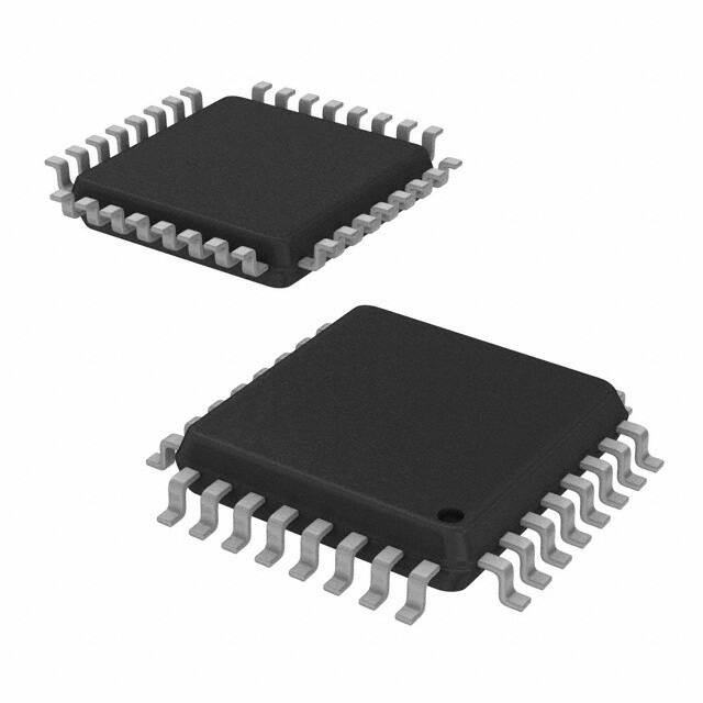
– 64-pin QFP/LQFP
– 44-pin LQFP
– 32-pin LQFP
KE02 Sub-Family Data Sheet, Rev. 7, 12/2019
2
NXP Semiconductors
�Table of Contents
1 Ordering parts.......................................................................................4
1.1 Determining valid orderable parts............................................... 4
5.2.2
FTM module timing....................................................... 17
5.3 Thermal specifications................................................................. 18
2 Part identification................................................................................. 4
5.3.1
Thermal operating requirements.................................... 18
2.1 Description...................................................................................4
5.3.2
Thermal characteristics.................................................. 18
2.2 Format.......................................................................................... 4
6 Peripheral operating requirements and behaviors................................ 20
2.3 Fields............................................................................................4
6.1 Core modules............................................................................... 20
2.4 Example....................................................................................... 5
6.1.1
SWD electricals .............................................................20
3 Parameter classification........................................................................5
6.2 External oscillator (OSC) and ICS characteristics.......................21
4 Ratings..................................................................................................6
6.3 NVM specifications..................................................................... 23
4.1 Thermal handling ratings............................................................. 6
6.4 Analog..........................................................................................24
4.2 Moisture handling ratings............................................................ 6
6.4.1
ADC characteristics....................................................... 24
4.3 ESD handling ratings................................................................... 6
6.4.2
Analog comparator (ACMP) electricals.........................27
4.4 Voltage and current operating ratings..........................................7
5 General................................................................................................. 7
5.1 Nonswitching electrical specifications........................................ 7
6.5 Communication interfaces........................................................... 27
6.5.1
SPI switching specifications.......................................... 27
7 Dimensions...........................................................................................31
5.1.1
DC characteristics.......................................................... 7
5.1.2
Supply current characteristics........................................ 14
8 Pinout................................................................................................... 32
5.1.3
EMC performance..........................................................15
8.1 Signal multiplexing and pin assignments.................................... 32
5.2 Switching specifications.............................................................. 16
8.2 Device pin assignment................................................................. 34
5.2.1
Control timing................................................................ 16
7.1 Obtaining package dimensions.................................................... 31
9 Revision history....................................................................................36
KE02 Sub-Family Data Sheet, Rev. 7, 12/2019
NXP Semiconductors
3
�Ordering parts
1 Ordering parts
1.1 Determining valid orderable parts
Valid orderable part numbers are provided on the web. To determine the orderable part
numbers for this device, go to nxp.com and perform a part number search for the
following device numbers: KE02Z.
2 Part identification
2.1 Description
Part numbers for the chip have fields that identify the specific part. You can use the
values of these fields to determine the specific part you have received.
2.2 Format
Part numbers for this device have the following format:
Q KE## A FFF R T PP CC N
2.3 Fields
This table lists the possible values for each field in the part number (not all combinations
are valid):
Field
Description
Values
Q
Qualification status
KE##
Kinetis family
• KE02
A
Key attribute
• Z = M0+ core
FFF
Program flash memory size
R
Silicon revision
• M = Fully qualified, general market flow
• P = Prequalification
• 16 = 16 KB
• 32 = 32 KB
• 64 = 64 KB
• (Blank) = Main
• A = Revision after main
Table continues on the next page...
KE02 Sub-Family Data Sheet, Rev. 7, 12/2019
4
NXP Semiconductors
�Parameter classification
Field
Description
T
Temperature range (°C)
PP
Package identifier
CC
Maximum CPU frequency (MHz)
N
Packaging type
Values
• V = –40 to 105
•
•
•
•
LC = 32 LQFP (7 mm x 7 mm)
LD = 44 LQFP (10 mm x 10 mm)
QH = 64 QFP (14 mm x 14 mm)
LH = 64 LQFP (10 mm x 10 mm)
• 2 = 20 MHz
• R = Tape and reel
• (Blank) = Trays
2.4 Example
This is an example part number:
MKE02Z64VQH2
3 Parameter classification
The electrical parameters shown in this supplement are guaranteed by various methods.
To give the customer a better understanding, the following classification is used and the
parameters are tagged accordingly in the tables where appropriate:
Table 1. Parameter classifications
P
Those parameters are guaranteed during production testing on each individual device.
C
Those parameters are achieved by the design characterization by measuring a statistically relevant sample size
across process variations.
T
Those parameters are achieved by design characterization on a small sample size from typical devices under
typical conditions unless otherwise noted. All values shown in the typical column are within this category.
D
Those parameters are derived mainly from simulations.
NOTE
The classification is shown in the column labeled “C” in the
parameter tables where appropriate.
KE02 Sub-Family Data Sheet, Rev. 7, 12/2019
NXP Semiconductors
5
�Ratings
4 Ratings
4.1 Thermal handling ratings
Symbol
Description
Min.
Max.
Unit
Notes
TSTG
Storage temperature
–55
150
°C
1
TSDR
Solder temperature, lead-free
—
260
°C
2
1. Determined according to JEDEC Standard JESD22-A103, High Temperature Storage Life.
2. Determined according to IPC/JEDEC Standard J-STD-020, Moisture/Reflow Sensitivity Classification for Nonhermetic
Solid State Surface Mount Devices.
4.2 Moisture handling ratings
Symbol
MSL
Description
Moisture sensitivity level
Min.
Max.
Unit
Notes
—
3
—
1
1. Determined according to IPC/JEDEC Standard J-STD-020, Moisture/Reflow Sensitivity Classification for Nonhermetic
Solid State Surface Mount Devices.
4.3 ESD handling ratings
Symbol
Description
Min.
Max.
Unit
Notes
VHBM
Electrostatic discharge voltage, human body model
–6000
+6000
V
1
VCDM
Electrostatic discharge voltage, charged-device model
–500
+500
V
2
Latch-up current at ambient temperature of 125°C
–100
+100
mA
3
ILAT
1. Determined according to JEDEC Standard JESD22-A114, Electrostatic Discharge (ESD) Sensitivity Testing Human Body
Model (HBM).
2. Determined according to JEDEC Standard JESD22-C101, Field-Induced Charged-Device Model Test Method for
Electrostatic-Discharge-Withstand Thresholds of Microelectronic Components.
3. Determined according to JEDEC Standard JESD78D, IC Latch-up Test.
• Test was performed at 125 °C case temperature (Class II).
• I/O pins pass ±100 mA I-test with IDD current limit at 800 mA.
• I/O pins pass +60/-100 mA I-test with IDD current limit at 1000 mA.
• Supply groups pass 1.5 Vccmax.
• RESET pin was only tested with negative I-test due to product conditioning requirement.
KE02 Sub-Family Data Sheet, Rev. 7, 12/2019
6
NXP Semiconductors
�General
4.4 Voltage and current operating ratings
Absolute maximum ratings are stress ratings only, and functional operation at the
maxima is not guaranteed. Stress beyond the limits specified in the following table may
affect device reliability or cause permanent damage to the device. For functional
operating conditions, refer to the remaining tables in this document.
This device contains circuitry protecting against damage due to high static voltage or
electrical fields; however, it is advised that normal precautions be taken to avoid
application of any voltages higher than maximum-rated voltages to this high-impedance
circuit. Reliability of operation is enhanced if unused inputs are tied to an appropriate
logic voltage level (for instance, either VSS or VDD) or the programmable pullup resistor
associated with the pin is enabled.
Table 2. Voltage and current operating ratings
Symbol
Description
Min.
Max.
Unit
VDD
Digital supply voltage
–0.3
6.0
V
IDD
Maximum current into VDD
—
120
mA
VIN
ID
VDDA
0.31
Input voltage except true open drain pins
–0.3
VDD +
Input voltage of true open drain pins
–0.3
6
V
Instantaneous maximum current single pin limit (applies to all
port pins)
–25
25
mA
VDD – 0.3
VDD + 0.3
V
Analog supply voltage
V
1. Maximum rating of VDD also applies to VIN.
5 General
5.1 Nonswitching electrical specifications
5.1.1 DC characteristics
This section includes information about power supply requirements and I/O pin
characteristics.
Table 3. DC characteristics
Symbol
—
C
—
Descriptions
Operating
voltage2
—
Min
Typical1
Max
Unit
2.7
—
5.5
V
Table continues on the next page...
KE02 Sub-Family Data Sheet, Rev. 7, 12/2019
NXP Semiconductors
7
�Nonswitching electrical specifications
Table 3. DC characteristics (continued)
Symbol
C
Descriptions
Min
Typical1
Max
Unit
VOH
P
Output All I/O pins, except PTA2 5 V, Iload = –5 mA
high
and PTA3, standard3 V, Iload = –2.5 mA
voltage
drive strength
VDD – 0.8
—
—
V
VDD – 0.8
—
—
V
C
P
High current drive pins,
high-drive strength3
5 V, Iload = –20 mA
VDD – 0.8
—
—
V
3 V, Iload = –10 mA
VDD – 0.8
—
—
V
Output
high
current
Max total IOH for all ports
5V
—
—
–100
mA
3V
—
—
–60
Output
low
voltage
All I/O pins, standarddrive strength
5 V, Iload = 5 mA
—
—
0.8
V
3 V, Iload = 2.5 mA
—
—
0.8
V
5 V, Iload =20 mA
—
—
0.8
V
3 V, Iload = 10 mA
—
—
0.8
V
5V
—
—
100
mA
3V
—
—
60
4.5≤VDD