NXP Semiconductors
Data Sheet: Technical Data
MKL28Z512Vxx7
Rev. 2.1, 06/2016
Kinetis KL28Zxxx with 512 KB
Flash and 128 KB SRAM
MKL28Z512Vxx7
72 MHz Cortex-M0+ based Microcontroller
Supports ultra low power ARM based microcontroller with
crystal-less USB feature, large flash and RAM, evolutionary lowpower peripherals and security features. This is an ideal solution
for Sensor Hub applications, Bluetooth, Wi-Fi connectivity, Smart
Energy, Internet of Things, and Edge and Concentrator. This
device offers:
• 128KB SRAM for data processing and connectivity stack
• Ultra low dynamic and static power consumption with smart
peripherals for low power applications
• Advanced LPI2C and LPSPI supporting asynchronous
DMA master data transition
• FlexIO for flexible and high performance interfaces
• Crypto acceleration with AES/DES/3DES/MD5/SHA and TRNG
• USB FS 2.0 device operation without need of external crystal
Core
• ARM® Cortex®-M0+ cores up to 72 MHz in Normal
mode and 96 MHz in High Speed mode
Memories
• Up to 512 KB program flash memory
• 128 KB SRAM
• 32 KB ROM with built-in bootloader
System peripherals
• 8-channel DMA controller
• Independent clocked Watchdog
• Low-leakage wakeup unit
• SWD debug interface and Micro Trace Buffer
• Bit Manipulation Engine
• Memory Mapped Divide and Square Root module
(MMDDVSQ)
• Cyclic Redundancy Check (CRC) module
• Nested Vector Interrupt Controller (NVIC) supports 32
interrupt vectors
• Additional peripheral interrupt support via Interrupt
Multiplexer (INTMUX)
Clocks
• System Clock Generator module that includes the
following clock sources:
• 48 to 60 MHz high accuracy fast internal
reference clock (FIRC)
121 XFBGA
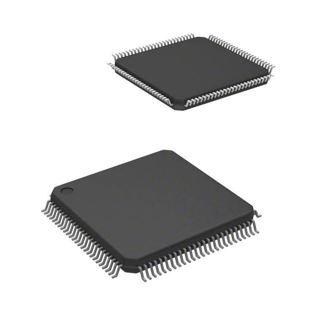
100 LQFP
8 x 8 x 0.43 mm Pitch 14 x 14 x 1.4 mm Pitch
0.65 mm
0.5 mm
Communication interfaces
• Three 16-bit Low Power Serial Peripheral Interface
(LPSPI) modules
• One EMVSIM module supporting EMV version 4.3,
ISO7816
• Three LPUART modules
• Three LPI2C modules supporting up to 5 Mbit/s
• One SAI module supporting I2S
• One FlexIO module emulating UART, SPI, I2S,
camera interface, and Motorola 68K/Intel 8080 bus
• USB FS 2.0 device operation without need of
external crystal
Analog Modules
• 16-bit, 24-channel SAR ADC with internal voltage
reference
• Two High-speed analog comparators each
containing a 6-bit DAC and programmable reference
input
• One 12-bit DAC
• 1.2 V and 2.1 V voltage references (Vref)
Timers
• One 6-channel Timer/PWM module
• Two 2-channel Timer/PWM modules
• Two low-power timers
• Two periodic interrupt timers
NXP reserves the right to change the production detail specifications as may be
required to permit improvements in the design of its products.
�•
•
•
•
32–40 kHz, or 3–32 MHz crystal oscillator
• Secure Real time clock
1 kHz LPO clock
• 56-bit software time stamp timer at 1 MHz
8/2 MHz slow internal reference clock (SIRC)
Security and integrity modules
Peripheral Clock Control (PCC) module that
• 80-bit unique identification number per chip
supports asynchronous clocking and clock divide
• MMCAU supports acceleration of the DES, 3DES,
options for peripherals.
AES, MD5, SHA-1, and SHA-256 algorithms
Human-machine interface
• True Random Number Generator (TRNG)
• General-purpose input/output up to 97
Operating Characteristics
• Low-power hardware touch sensor interface (TSI)
• Voltage range: 1.71 to 3.6 V
• Temperature range: –40 to 105 °C
NOTE
The 121-pin packages for this product is not yet available. However, it is included in a
Package Your Way program for Kinetis MCUs. Visit nxp.com/KPYW for more
details.
Ordering Information 1
Part Number
Memory
Package
IO and ADC channels
Flash (KB)
SRAM (KB)
Pin count
Package
GPIOs
GPIOs
(INT/HD)
ADC
channels
(SE/DP)
MKL28Z512V
LL7
512
128
100
LQFP
82
82/8
27/4
MKL28Z512V
DC72
512
128
121
XFBGA
97
97/8
27/4
1. To confirm current availability of ordererable part numbers, go to http://www.nxp.com and perform a part number search.
2. Package Your Way.
Related Resources
Type
Description
Resource
Selector
Guide
The NXP Solution Advisor is a web-based tool that features interactive
application wizards and a dynamic product selector.
Solution Advisor
Product Brief
The Product Brief contains concise overview/summary information to
enable quick evaluation of a device for design suitability.
KL2XPB1
Reference
Manual
The Reference Manual contains a comprehensive description of the
structure and function (operation) of a device.
MKL28ZRM1
Data Sheet
The Data Sheet includes electrical characteristics and signal
connections.
MKL28Z512Vxx71
Chip Errata
The chip mask set Errata provides additional or corrective information for KINETIS_L_1N52N1
a particular device mask set.
Package
drawing
Package dimensions are provided in package drawings.
• 121-XFBGA:
98ASA00595D1
• 100-LQFP:
98ASS23308W1
1. To find the associated resource, go to http://www.nxp.com and perform a search using this term.
2
NXP Semiconductors
Kinetis KL28Zxxx with 512 KB Flash and 128 KB SRAM, Rev. 2.1, 06/2016
�Timer
Timer
TSTMR
0
TPM
2
Timer
Timer
WDOG
Reset
SPI
UART
LPSPI
2
LPUART
2
Clocks/
Oscillators
ANALOG
SCG
XTAL
OSC
ADC
Inputs
ADC0
Temp
Monitor
FIRC
SIRC
DAC
Outputs
DAC0
VREF
PLL
LPO1K
CAU
SIM
s2
Cortex-M0+
Platform
MTB
IO Port
SYSTICK
CTI
DBG
AHB-AP0
NVIC
s1
m0
MPU
System
Interrupts
AWIC
m2
UART
BME
mux
TRG
MUX
FlexIO
8/16-bit
Parallel I/F
FlexIO0
Audio
RGPIO
GPIO
SRAM
128KB
EMVSIM
LPUART
0/1
LPI2C
0/1
SAI0
AHB
PCC
I2C
I2C
FLASH 0
256KB
FLASH 1
256KB
FMC
TRNG
LPSPI
0/1
LPI2C
2
FTFA
BME
SPI
TPM
0/1
TSI
s3
M0+ DBG
Timer
TSI0
ROM
32KB
s0
CTI
AIPS1
SMC
MSCM
m1
AXBS
Cortex-M0+
DWT
MDM-AP
LLWU
0
•• DMA
• Requests
DMAMux
0
Core
DVSQ
SWD-DP
RCM
DMA0
8-channel
MCM
USBVREG
LPIT
0
SRAM
+PPB CTRL
USB
SRTC
SCG
TRG
MUX
SWD
LPTMR WDOG
0
0
PCC
CMP0
CMP1
LPTMR
1
CRC
INTMUX0
Reference
Inputs
PMC
USB
SRAM
EMVSIM
PortA
Port A
PortB
Port B
PortC
Port C
PortD
Port D
PortE
Port E
USB0
1x
USB
AIPS0
LEGEND:
S
DAP
Synchronizer
Reference
sec Memory protection
exsc Gaskets
Bus Components
Core MemoryMapped Module
Other Module such
as test/analog
Platform Domain
CM0+ Platform
AHB32
AIPS0 IPBUS
AIPS1 IPBUS
Analog Domain
Figure 1. KL28Z block diagram
Kinetis KL28Zxxx with 512 KB Flash and 128 KB SRAM, Rev. 2.1, 06/2016
3
NXP Semiconductors
�Table of Contents
1 Ratings.................................................................................. 5
1.1 Thermal handling ratings............................................... 5
1.2 Moisture handling ratings...............................................5
1.3 ESD handling ratings..................................................... 5
1.4 Voltage and current operating ratings............................5
2 General................................................................................. 6
2.1 AC electrical characteristics...........................................6
2.2 Nonswitching electrical specifications............................7
2.2.1 Voltage and current operating requirements..... 7
2.2.2 LVD, HVD, and POR operating requirements... 7
2.2.3 Voltage and current operating behaviors...........8
2.2.4 Power mode transition operating behaviors...... 9
2.2.5 Power consumption operating behaviors.......... 10
2.2.6 EMC radiated emissions operating behaviors... 19
2.2.7 Designing with radiated emissions in mind........20
2.2.8 Capacitance attributes.......................................20
2.3 Switching specifications.................................................20
2.3.1 Device clock specifications................................20
2.3.2 General switching specifications....................... 21
2.4 Thermal specifications................................................... 23
2.4.1 Thermal operating requirements....................... 23
2.4.2 Thermal attributes..............................................23
3 Peripheral operating requirements and behaviors................ 24
3.1 Core modules................................................................ 24
3.1.1 SWD electricals ................................................ 24
3.2 System modules............................................................ 26
3.3 Clock modules............................................................... 26
3.3.1 System Clock Generation (SCG) specifications 26
3.3.2 Oscillator electrical specifications...................... 28
3.4 Memories and memory interfaces................................. 30
3.4.1 Flash electrical specifications............................ 30
3.5 Security and integrity modules.......................................32
3.6 Analog............................................................................32
3.6.1 ADC electrical specifications............................. 32
3.6.2 Voltage reference electrical specifications........ 36
3.6.3 CMP and 6-bit DAC electrical specifications..... 38
3.6.4 12-bit DAC electrical characteristics.................. 40
3.7 Timers............................................................................43
4
NXP Semiconductors
4
5
6
7
8
9
3.8 Communication interfaces............................................. 43
3.8.1 EMV SIM specifications.....................................43
3.8.2 USB electrical specifications............................. 48
3.8.3 USB VREG electrical specifications.................. 49
3.8.4 LPSPI switching specifications.......................... 49
3.8.5 LPI2C.................................................................54
3.8.6 LPUART............................................................ 54
3.8.7 I2S/SAI switching specifications........................ 55
3.9 Human-machine interfaces (HMI)..................................59
3.9.1 TSI electrical specifications............................... 59
Dimensions........................................................................... 59
4.1 Obtaining package dimensions......................................59
Pinouts and Packaging......................................................... 60
5.1 KL28Z Signal Multiplexing and Pin Assignments.......... 60
5.2 KL28Z Pinouts............................................................... 65
Ordering parts....................................................................... 67
6.1 Determining valid orderable parts..................................67
Design considerations...........................................................68
7.1 Hardware design considerations................................... 68
7.1.1 Printed circuit board recommendations............. 68
7.1.2 Power delivery system.......................................68
7.1.3 Analog design....................................................69
7.1.4 Digital design..................................................... 70
7.1.5 Crystal oscillator................................................ 74
7.2 Software considerations................................................ 75
Part identification...................................................................76
8.1 Description.....................................................................76
8.2 Format........................................................................... 76
8.3 Fields............................................................................. 76
8.4 Example.........................................................................77
Terminology and guidelines.................................................. 77
9.1 Definitions...................................................................... 77
9.2 Examples....................................................................... 78
9.3 Typical-value conditions................................................ 78
9.4 Relationship between ratings and operating
requirements..................................................................79
9.5 Guidelines for ratings and operating requirements........79
10 Revision History.................................................................... 80
Kinetis KL28Zxxx with 512 KB Flash and 128 KB SRAM, Rev. 2.1, 06/2016
�Ratings
1 Ratings
1.1 Thermal handling ratings
Table 1. Thermal handling ratings
Symbol
Description
Min.
Max.
Unit
Notes
TSTG
Storage temperature
–55
150
°C
1
TSDR
Solder temperature, lead-free
—
260
°C
2
1. Determined according to JEDEC Standard JESD22-A103, High Temperature Storage Life.
2. Determined according to IPC/JEDEC Standard J-STD-020, Moisture/Reflow Sensitivity Classification for Nonhermetic
Solid State Surface Mount Devices.
1.2 Moisture handling ratings
Table 2. Moisture handling ratings
Symbol
MSL
Description
Moisture sensitivity level
Min.
Max.
Unit
Notes
—
3
—
1
1. Determined according to IPC/JEDEC Standard J-STD-020, Moisture/Reflow Sensitivity Classification for Nonhermetic
Solid State Surface Mount Devices.
1.3 ESD handling ratings
Table 3. ESD handling ratings
Symbol
Description
Min.
Max.
Unit
Notes
VHBM
Electrostatic discharge voltage, human body model
–2000
+2000
V
1
VCDM
Electrostatic discharge voltage, charged-device
model
–500
+500
V
2
Latch-up current at ambient temperature of 105 °C
–100
+100
mA
3
ILAT
1. Determined according to JEDEC Standard JESD22-A114, Electrostatic Discharge (ESD) Sensitivity Testing Human
Body Model (HBM).
2. Determined according to JEDEC Standard JESD22-C101, Field-Induced Charged-Device Model Test Method for
Electrostatic-Discharge-Withstand Thresholds of Microelectronic Components.
3. Determined according to JEDEC Standard JESD78, IC Latch-Up Test.
Kinetis KL28Zxxx with 512 KB Flash and 128 KB SRAM, Rev. 2.1, 06/2016
5
NXP Semiconductors
�General
1.4 Voltage and current operating ratings
Table 4. Voltage and current operating ratings
Symbol
Description
Min.
Max.
Unit
VDD
Digital supply voltage
–0.3
3.8
V
IDD
Digital supply current
—
120
mA
VIO
IO pin input voltage
–0.3
VDD + 0.3
V
Instantaneous maximum current single pin limit (applies to
all port pins)
–25
25
mA
ID
VDDA
Analog supply voltage
VDD – 0.3
VDD + 0.3
V
VUSB_DP
USB_DP input voltage
–0.3
3.63
V
VUSB_DM
USB_DM input voltage
–0.3
3.63
V
USB regulator input
–0.3
6.0
V
VREGIN
2 General
2.1 AC electrical characteristics
Unless otherwise specified, propagation delays are measured from the 50% to the 50%
point, and rise and fall times are measured at the 20% and 80% points, as shown in the
following figure.
VIH
Input Signal
Low
High
80%
50%
20%
Midpoint1
Fall Time
VIL
Rise Time
The midpoint is VIL + (VIH - VIL) / 2
Figure 2. Input signal measurement reference
All digital I/O switching characteristics, unless otherwise specified, assume that the
output pins have the following characteristics.
• CL=30 pF loads
• Slew rate disabled
• Normal drive strength
6
NXP Semiconductors
Kinetis KL28Zxxx with 512 KB Flash and 128 KB SRAM, Rev. 2.1, 06/2016
�General
2.2 Nonswitching electrical specifications
2.2.1 Voltage and current operating requirements
Table 5. Voltage and current operating requirements
Symbol
Description
Min.
Max.
Unit
VDD
Supply voltage
1.71
3.6
V
VDDA
Analog supply voltage
1.71
3.6
V
VDD – VDDA VDD-to-VDDA differential voltage
–0.1
0.1
V
VSS – VSSA VSS-to-VSSA differential voltage
–0.1
0.1
V
• 2.7 V ≤ VDD ≤ 3.6 V
0.7 × VDD
—
V
• 1.71 V ≤ VDD ≤ 2.7 V
0.75 × VDD
—
V
• 2.7 V ≤ VDD ≤ 3.6 V
—
0.35 × VDD
V
• 1.71 V ≤ VDD ≤ 2.7 V
—
0.3 × VDD
V
0.06 × VDD
—
V
-5
—
mA
-25
—
mA
VIH
VIL
Input high voltage
Input low voltage
VHYS
Input hysteresis
IICIO
IO pin negative DC injection current — single pin
1
• VIN < VSS-0.3V
IICcont
Notes
Contiguous pin DC injection current —regional limit,
includes sum of negative injection currents of 16
contiguous pins
• Negative current injection
VODPU
Open drain pullup voltage level
VDD
VDD
V
VRAM
VDD voltage required to retain RAM
1.2
—
V
2
1. All I/O pins are internally clamped to VSS through a ESD protection diode. There is no diode connection to VDD. If VIN
greater than VIO_MIN (= VSS-0.3 V) is observed, then there is no need to provide current limiting resistors at the pads. If
this limit cannot be observed then a current limiting resistor is required. The negative DC injection current limiting
resistor is calculated as R = (VIO_MIN - VIN)/|IICIO|.
2. Open drain outputs must be pulled to VDD.
2.2.2 LVD, HVD, and POR operating requirements
Table 6. VDD supply LVD, HVD, and POR operating requirements
Symbol
VPOR
Description
Min.
Typ.
Max.
Unit
Notes
Falling VDD POR detect voltage
0.8
1.1
1.5
V
—
Table continues on the next page...
Kinetis KL28Zxxx with 512 KB Flash and 128 KB SRAM, Rev. 2.1, 06/2016
7
NXP Semiconductors
�General
Table 6. VDD supply LVD, HVD, and POR operating requirements (continued)
Symbol
VLVDH
Description
Min.
Typ.
Max.
Unit
Notes
Falling low-voltage detect threshold — high
range (LVDV = 01)
2.48
2.56
2.64
V
—
Low-voltage warning thresholds — high range
VLVW1H
• Level 1 falling (LVWV = 00)
VLVW2H
• Level 2 falling (LVWV = 01)
VLVW3H
• Level 3 falling (LVWV = 10)
VLVW4H
• Level 4 falling (LVWV = 11)
VHYSH
Low-voltage inhibit reset/recover hysteresis —
high range
VLVDL
Falling low-voltage detect threshold — low
range (LVDV=00)
1
2.62
2.70
2.78
V
2.72
2.80
2.88
V
2.82
2.90
2.98
V
2.92
3.00
3.08
V
—
±60
—
mV
—
1.54
1.60
1.66
V
—
Low-voltage warning thresholds — low range
VLVW1L
• Level 1 falling (LVWV = 00)
VLVW2L
• Level 2 falling (LVWV = 01)
VLVW3L
• Level 3 falling (LVWV = 10)
VLVW4L
• Level 4 falling (LVWV = 11)
VHYSL
Low-voltage inhibit reset/recover hysteresis —
low range
1
1.74
1.80
1.86
V
1.84
1.90
1.96
V
1.94
2.00
2.06
V
2.04
2.10
2.16
V
—
±40
—
mV
—
VBG
Bandgap voltage reference
0.97
1.00
1.03
V
—
tLPO
Internal low power oscillator period — factory
trimmed
900
1000
1100
μs
—
High voltage detect threshold — low range
(HVDV=0) — Rising
3.4
3.5
3.6
V
2
High voltage detect threshold — low range
(HVDV=0) — Falling
3.35
3.45
3.55
High voltage detect threshold — high range
(HVDV=1) — Rising
3.65
3.75
3.85
V
2
High voltage detect threshold — high range
(HVDV=1) — Falling
3.6
3.7
3.8
High voltage detect hysteresis — low range
(HVDV=0)
—
50
—
mV
—
High voltage detect hysteresis — high range
(HVDV=1)
—
50
—
VHVDL
VHVDH
VHYSH
1. Rising thresholds are falling threshold + hysteresis voltage
2. The selection of high voltage detect trip voltage is controlled by PMC_HVDSC1[HVDV].
8
NXP Semiconductors
Kinetis KL28Zxxx with 512 KB Flash and 128 KB SRAM, Rev. 2.1, 06/2016
�General
2.2.3 Voltage and current operating behaviors
Table 7. Voltage and current operating behaviors
Symbol
VOH
Description
• 1.71 V ≤ VDD ≤ 2.7 V, IOH = –2.5 mA
Max.
Unit
• 1.71 V ≤ VDD ≤ 2.7 V, IOH = –10 mA
IOHT
Output high current total for all ports
VOL
Output low voltage — Normal drive pad
Notes
1
VDD – 0.5
—
V
VDD – 0.5
—
V
Output high voltage — High drive pad
• 2.7 V ≤ VDD ≤ 3.6 V, IOH = –20 mA
VOL
Typ.
Output high voltage — Normal drive pad
• 2.7 V ≤ VDD ≤ 3.6 V, IOH = –5 mA
VOH
Min.
1
VDD – 0.5
—
V
VDD – 0.5
—
V
—
100
mA
1
• 2.7 V ≤ VDD ≤ 3.6 V, IOL = 5 mA
—
0.5
V
• 1.71 V ≤ VDD ≤ 2.7 V, IOL = 2.5 mA
—
0.5
V
Output low voltage — High drive pad
1
• 2.7 V ≤ VDD ≤ 3.6 V, IOL = 20 mA
—
0.5
V
• 1.71 V ≤ VDD ≤ 2.7 V, IOL = 10 mA
—
0.5
V
Output low current total for all ports
—
100
mA
IIN
Input leakage current (per pin) for full
temperature range
—
1
μA
2
IIN
Input leakage current (per pin) at 25 °C
—
0.025
μA
2
IIN
Input leakage current (total all pins) for full
temperature range
—
41
μA
2
IOZ
Hi-Z (off-state) leakage current (per pin)
—
1
μA
RPU
Internal pullup resistors
20
50
kΩ
IOLT
3
1. PTB0, PTB1, PTC3, PTC4, PTD4, PTD5, PTD6 and PTD7 I/O have both high drive and normal drive capability
selected by the associated PORTx_PCRn[DSE] control bit. All other GPIOs are normal drive only. PTD4, PTD5,
PTD6, PTD7, PTE20, PTE21, PTE22, and PTE23 are also fast pins.
2. Measured at VDD = 3.6 V
3. Measured at VDD supply voltage = VDD min and Vinput = VSS
2.2.4 Power mode transition operating behaviors
All specifications in the following table assume this clock configuration in Run mode:
• CPU and system clocks = 48 MHz
• Bus and flash clock = 24 MHz
• SCG configured in FIRC mode; peripheral functional clocks from
FIRCDIV3_CLK and USB clock from FIRCDIV1_CLK
Kinetis KL28Zxxx with 512 KB Flash and 128 KB SRAM, Rev. 2.1, 06/2016
9
NXP Semiconductors
�General
Table 8. Power mode transition operating behaviors
Symbol
tPOR
Description
After a POR event, amount of time from the
point VDD reaches 1.8 V to execution of the first
instruction across the operating temperature
range of the chip.
Min.
Typ.
Max.
Unit
Notes
—
—
300
μs
1
—
188
193
μs
—
188
193
μs
—
125
130
μs
—
125
130
μs
—
5.5
6.1
μs
—
5.5
6.1
μs
—
5.5
6.1
μs
—
5.5
6.1
μs
• VLLS0 → RUN
• VLLS1 → RUN
• VLLS2 → RUN
• VLLS3 → RUN
• LLS3 → RUN
• LLS2 → RUN
• VLPS → RUN
• STOP → RUN
1. Normal boot (FTFA_FOPT[LPBOOT]=11).
2.2.5 Power consumption operating behaviors
NOTE
The values in the following table are based on
characterization data with a few samples.
NOTE
The actual power consumption measured in the related
condition, with certain peripherals running, is the sum of
related low power current consumption of the device listed in
Table 9 and the related low power mode peripheral adders in
Table 10.
10
NXP Semiconductors
Kinetis KL28Zxxx with 512 KB Flash and 128 KB SRAM, Rev. 2.1, 06/2016
�General
NOTE
The maximum values represent characterized results
equivalent to the mean plus three times the standard
deviation (mean + 3σ).
Table 9. Power consumption operating behaviors
Symbol
IDDA
IDD_HSRUN
IDD_HSRUN
IDD_RUN
Description
Analog supply current
IDD_RUN
Max.
Unit
Notes
—
—
See note
mA
1
2
• at 1.8 V
—
12.6
17.4
mA
• at 3.0 V
—
12.8
17.6
mA
High speed run mode current at 96
MHz - all peripheral clocks enabled,
code executing from flash, while(1)
loop
3
• at 1.8 V
—
15.5
20.4
mA
• at 3.0 V
—
15.7
20.6
mA
Run mode current at 72 MHz - all
peripheral clocks disabled, code
executing from flash, while(1) loop
• at 3.0 V
IDD_RUN
Typ.
High speed run mode current at 96
MHz - all peripheral clocks disabled,
code executing from flash, while(1)
loop
• at 1.8 V
IDD_RUN
Min.
4
—
9.4
13.6
mA
—
9.6
13.8
mA
Run mode current at 48 Mhz - all
peripheral clocks disabled, code
executing from flash, while(1) loop
5
• at 1.8 V
—
7.3
11.4
mA
• at 3.0 V
—
7.4
11.5
mA
Run mode current at 72 MHz - all
peripheral clocks enabled, code
executing from flash, while(1) loop
6
• at 1.8 V
—
11.6
15.9
mA
• at 3.0 V
—
11.7
16.0
mA
Run mode current at 48 Mhz - all
peripheral clocks enabled, code
executing from flash, while(1) loop
7
• at 1.8 V
—
8.9
13.1
mA
• at 3.0 V
—
9.1
13.3
mA
Table continues on the next page...
Kinetis KL28Zxxx with 512 KB Flash and 128 KB SRAM, Rev. 2.1, 06/2016
11
NXP Semiconductors
�General
Table 9. Power consumption operating behaviors (continued)
Symbol
Description
Min.
Typ.
Max.
Unit
Notes
IDD_WAIT
Wait mode high frequency current at 72
MHz, at 3.0 V - all peripheral clocks
disabled, while(1) loop
—
7.0
9.0
mA
4
IDD_WAIT
Wait mode current at 3.0 V at 48 Mhz
— all peripheral clocks disabled,
while(1) loop
—
5.7
10.4
mA
5
IDD_VLPR
Very-low-power run mode current at
3.0 V — all peripheral clocks enabled
at 4 MHz, while(1) loop
—
483.7
1011.7
μA
8
IDD_VLPR
Very-low-power run mode current at
3.0 V — all peripheral clocks enabled
at 8 MHz, while(1) loop
—
557.6
1720.2
μA
9
IDD_VLPR
Very-low-power run mode current at
3.0 V — all peripheral clocks disabled
at 4 MHz, while(1) loop
—
400.3
926.5
μA
10
IDD_VLPR
Very-low-power run mode current at
3.0 V — all peripheral clocks disabled
at 8 MHz, while(1) loop
—
415.2
941.1
μA
11
IDD_VLPW
Very-low-power wait mode current at
3.0 V — all peripheral clocks disabled
at 4 MHz, while(1) loop
—
285.9
1145.6
μA
10
IDD_VLPW
Very-low-power wait mode current at
3.0 V — all peripheral clocks disabled
at 8 MHz, while(1) loop
—
415.6
1498.7
μA
11
IDD_STOP
Stop mode current at 3.0 V
• -40 to 25 °C
—
264.5
320.5
μA
• at 50 °C
—
287.0
356.1
• at 70 °C
—
325.3
445.4
• at 85 °C
—
374.7
590.8
• at 105 °C
—
496.7
952.3
—
4.2
16.4
—
11.0
35.9
—
24.0
84.5
—
44.0
156.2
—
93.4
300.2
—
2.7
5.4
—
4.7
10.6
—
8.6
22.7
—
14.7
49.0
IDD_VLPS
Very-low-power stop mode current at
3.0 V
• -40 to 25 °C
• at 50 °C
• at 70 °C
• at 85 °C
• at 105 °C
IDD_LLS2
Low-leakage stop mode 2 current at
3.0 V
• -40 to 25 °C
• at 50 °C
• at 70 °C
μA
μA
Table continues on the next page...
12
NXP Semiconductors
Kinetis KL28Zxxx with 512 KB Flash and 128 KB SRAM, Rev. 2.1, 06/2016
�General
Table 9. Power consumption operating behaviors (continued)
Symbol
Description
Min.
Typ.
Max.
—
30.4
88.6
—
3.0
5.9
—
5.9
14.5
—
11.4
32.0
—
19.7
65.2
—
40.9
122.0
• -40 to 25 °C
—
2.2
5.1
• at 50 °C
—
4.6
10.9
• at 70 °C
—
9.0
24.4
• at 85 °C
—
15.9
44.8
• at 105 °C
—
33.1
91.0
—
1.8
3.4
—
3.3
6.8
—
6.1
14.5
—
10.4
26.4
—
21.6
54.4
—
0.65
0.88
• at 50 °C
—
1.1
1.6
• at 70 °C
—
2.1
3.3
• at 85 °C
—
3.6
21.0
• at 105 °C
—
8.5
32.2
—
372.0
598
—
768.6
1331
—
1734
3038
—
3291
20575
—
8025
27560
• at 85 °C
Unit
Notes
• at 105 °C
IDD_LLS3
Low-leakage stop mode 3 current at
3.0 V
• -40 to 25 °C
• at 50 °C
• at 70 °C
• at 85 °C
• at 105 °C
IDD_VLLS3
IDD_VLLS2
Very-low-leakage stop mode 3 current
at 3.0 V
• at 50 °C
• at 70 °C
• at 85 °C
• at 105 °C
IDD_VLLS0
μA
Very-low-leakage stop mode 2 current
at 3.0 V
• -40 to 25 °C
IDD_VLLS1
μA
Very-low-leakage stop mode 1 current
at 3.0V
• -40 to 25 °C
Very-low-leakage stop mode 0 current
(SMC_STOPCTRL[PORPO] = 0) at 3.0
V
• -40 to 25 °C
• at 50 °C
• at 70 °C
μA
μA
nA
Table continues on the next page...
Kinetis KL28Zxxx with 512 KB Flash and 128 KB SRAM, Rev. 2.1, 06/2016
13
NXP Semiconductors
�General
Table 9. Power consumption operating behaviors (continued)
Symbol
Description
Min.
Typ.
Max.
Unit
Notes
• at 85 °C
• at 105 °C
IDD_VLLS0
Very-low-leakage stop mode 0 current
(SMC_STOPCTRL[PORPO] = 1) at 3.0
V
• -40 to 25 °C
• at 50 °C
• at 70 °C
• at 85 °C
• at 105 °C
12
—
94.1
311
—
480.9
1024
—
1416
2760
—
2970
19574
—
7642
27325
nA
1. The analog supply current is the sum of the active or disabled current for each of the analog modules on the device. See
each module's specification for its supply current.
2. 96 MHz core and system clock (DIVCORE_CLK), 24 MHz bus/slow clock(DIVSLOW_CLK), and 24 MHz flash clock.
SCG configured as System PLL mode (SCG_HCCR[SCS]=0110), PLL clock source is SOSC from external 8 MHz
crystal. All peripheral functional clocks disabled by clearing all xxDIV3, xxDIV2, and xxDIV1 in SCG_SOSCDIV and
SCG_SPLLDIV registers. FIRC and SIRC disabled by clearing SCG_FIRCCSR[FIRCEN] and SCG_SIRCCSR[SIRCEN].
3. 96 MHz core and system clock (DIVCORE_CLK), 24 MHz bus/slow clock(DIVSLOW_CLK), and 24 MHz flash clock.
SCG configured as System PLL mode (SCG_HCCR[SCS]=0110), PLL clock source is SOSC from external 8 MHz
crystal. All peripheral functional clocks except USB = 24 MHz from SPLLDIV3_CLK. USB functional clock = 48 MHz
from SPLLDIV1_CLK. FIRC and SIRC disabled by clearing SCG_FIRCCSR[FIRCEN] and SCG_SIRCCSR[SIRCEN].
4. 72 MHz core and system clock (DIVCORE_CLK), 24 MHz bus/slow clock(DIVSLOW_CLK), and 24 MHz flash clock.
SCG configured as System PLL mode (SCG_RCCR[SCS]=0110), PLL clock source is SOSC from external 8 MHz
crystal. All peripheral functional clocks disabled by clearing all xxDIV3, xxDIV2, and xxDIV1 in SCG_SOSCDIV and
SCG_SPLLDIV registers. FIRC and SIRC disabled by clearing SCG_FIRCCSR[FIRCEN] and SCG_SIRCCSR[SIRCEN].
5. 48 MHz core and system clock (DIVCORE_CLK), 24 MHz bus/slow clock(DIVSLOW_CLK), and 24 MHz flash clock.
SCG configured as FIRC 48 MHz mode (SCG_RCCR[SCS]=0011). All peripheral functional clocks disabled by clearing
all xxDIV3, xxDIV2, and xxDIV1 in SCG_FIRCDIV register. PLL, SOSC, and SIRC disabled by clearing
SCG_SPLLCSR[SPLLEN], SCG_SOSCCSR[SOSCEN], and SCG_SIRCCSR[SIRCEN].
6. 72 MHz core and system clock (DIVCORE_CLK), 24 MHz bus/slow clock(DIVSLOW_CLK), and 24 MHz flash clock.
SCG configured as System PLL mode (SCG_RCCR[SCS]=0110), PLL clock source is SOSC from external 8 MHz
crystal. All peripheral functional clocks except USB = 24 MHz from SPLLDIV3_CLK. USB functional clock = 48 MHz
from SPLLDIV1_CLK. FIRC and SIRC disabled by clearing SCG_FIRCCSR[FIRCEN] and SCG_SIRCCSR[SIRCEN].
7. 48 MHz core and system clock (DIVCORE_CLK), 24 MHz bus/slow clock(DIVSLOW_CLK), and 24 MHz flash clock.
SCG configured as FIRC 48 MHz mode (SCG_RCCR[SCS]=0011). All peripheral functional clocks except USB = 24
MHz from FIRCDIV3_CLK. USB functional clock = 48 MHz from FIRCDIV1_CLK. PLL, SOSC, and SIRC disabled by
clearing SCG_SPLLCSR[SPLLEN], SCG_SOSCCSR[SOSCEN], and SCG_SIRCCSR[SIRCEN].
8. 4 MHz core and system clock (DIVCORE_CLK), 1 MHz bus/slow clock(DIVSLOW_CLK), and 1 MHz flash clock. SCG
configured as SIRC 8 MHz mode (SCG_VCCR[SCS]=0010). All peripheral functional clocks except USB = 1M Hz from
SIRCDIV3_CLK. USB clock disabled. PLL, SOSC, and FIRC disabled by clearing SCG_SPLLCSR[SPLLEN],
SCG_SOSCCSR[SOSCEN], and SCG_FIRCCSR[FIRCEN].
9. 8 MHz core and system clock (DIVCORE_CLK), 1 MHz bus/slow clock(DIVSLOW_CLK), and 1 MHz flash clock. SCG
configured as SIRC 8 MHz mode (SCG_VCCR[SCS]=0010). All peripheral functional clocks except USB = 1M Hz from
SIRCDIV3_CLK. USB clock disabled. PLL, SOSC, and FIRC disabled by clearing SCG_SPLLCSR[SPLLEN],
SCG_SOSCCSR[SOSCEN], and SCG_FIRCCSR[FIRCEN].
10. 4 MHz core and system clock (DIVCORE_CLK), 1 MHz bus/slow clock(DIVSLOW_CLK), and 1 MHz flash clock. SCG
configured as SIRC 8 MHz mode (SCG_VCCR[SCS]=0010). All peripheral functional clocks disabled by clearing all
xxDIV3, xxDIV2, and xxDIV1 in SCG_SIRCDIV register. PLL, SOSC, and FIRC disabled by clearing
SCG_SPLLCSR[SPLLEN], SCG_SOSCCSR[SOSCEN], and SCG_FIRCCSR[FIRCEN].
11. 8 MHz core and system clock (DIVCORE_CLK), 1 MHz bus/slow clock(DIVSLOW_CLK), and 1 MHz flash clock. SCG
configured as SIRC 8 MHz mode (SCG_VCCR[SCS]=0010). All peripheral functional clocks disabled by clearing all
14
NXP Semiconductors
Kinetis KL28Zxxx with 512 KB Flash and 128 KB SRAM, Rev. 2.1, 06/2016
�General
xxDIV3, xxDIV2, and xxDIV1 in SCG_SIRCDIV register. PLL, SOSC, and FIRC disabled by clearing
SCG_SPLLCSR[SPLLEN], SCG_SOSCCSR[SOSCEN], and SCG_FIRCCSR[FIRCEN].
12. No brownout
Table 10. Low power mode peripheral adders — typical value
Symbol
Description
Temperature (°C)
-40
IEREFSTEN8MHz
External 8 MHz crystal clock adder with 402.9
System OSC. Measured by entering
VLPS mode with the crystal enabled
(SCG_SOSCCFG[RANGE] = 10,
SCG_SOSCCFG[HGO] = 0,
SCG_SOSCCFG[EREFS] = 1, and
SC2P/SC4P/SC8P = 0).
IEREFSTEN32KHz
External 32 kHz crystal clock adder
with System OSC by means of
SCG_SOSCCFG[RANGE] = 01,
SCG_SOSCCFG[HGO] = 0,
SCG_SOSCCFG[EREFS] = 1, and
SC2P/SC4P/SC8P = 0. Measured by
entering all the following modes with
the crystal enabled:
• VLLS1
Unit
25
50
70
85
105
462.1
477.5
492
506.2
530.4
uA
nA
373.9
539.2
612.3
644.9
523.7
1000
568.4
552.6
650.8
757.9
995.6
1400
• VLLS3
582.8
565.0
615.5
797.1
968.5
1700
• LLS3
472.4
635.2
776.9
425.6
1500
2800
• VLPS
528.0
534.1
636.6
9600
20300 40900
• STOP
ILPTMR
LPTMR peripheral adder measured by
placing the device in VLLS1 mode with
LPTMR enabled using LPO clock.
151.0
7.7
21.8
7.6
174.0
31.0
nA
ICMP
CMP peripheral adder measured by
placing the device in VLLS1 mode with
CMP enabled using the 6-bit DAC and
a single external input for compare.
Includes 6-bit DAC power
consumption.
18.8
19.6
19.9
20.0
20.4
20.5
µA
IRTC
RTC peripheral adder measured by
placing the device in VLLS1 mode and
the RTC ALARM set for 1 minute.
Includes selected clock source power
consumption.
• OSC32KCLK (32KHz external
crystal)
• LPO (internal 1K Hz Low Power
Oscillator)
116.0
1400
1400
1500
1500
120.0
nA
35.0
1400
1400
1600
1400
120.0
ILPUART
LPUART peripheral adder measured
by placing the device in STOP mode
with selected clock source waiting for
RX data at 115200 baud rate. Includes
Table continues on the next page...
Kinetis KL28Zxxx with 512 KB Flash and 128 KB SRAM, Rev. 2.1, 06/2016
15
NXP Semiconductors
�General
Table 10. Low power mode peripheral adders — typical value (continued)
Symbol
Description
Temperature (°C)
selected clock source power
consumption.
• Slow IRC clock from SCG (8
MHz internal reference clock)
• OSCERCLK (8 MHz external
crystal)
ILPSPI
ITPM
ILPI2C
IBG
LPSPI peripheral adder measured by
placing the device in VLPS mode with
selected clock source, LPSPI is
configured as master mode with bit
rate of 4 Mbps. Includes selected clock
source power consumption.
• Slow IRC clock from SCG (8
MHz internal reference clock)
• OSCERCLK (8 MHz external
crystal)
TPM peripheral adder measured by
placing the device in STOP mode with
selected clock source configured for
output compare generating 100 Hz
clock signal. No load is placed on the
I/O generating the clock signal.
Includes selected clock source and I/O
switching currents.
• Slow IRC clock from SCG (8
MHz internal reference clock)
• OSCERCLK (8 MHz external
crystal)
LPI2C peripheral adder measured by
placing the device in VLPS mode with
selected clock source, LPI2C is
configured as master, and bit rate is
400 Kbps. Includes selected clock
source power consumption.
• Slow IRC clock from SCG (8
MHz internal reference clock)
• OSCERCLK (8 MHz external
crystal)
Bandgap adder when BGEN bit is set
and device is placed in VLPS mode.
• Bandgap buffer disabled
• Bandgap buffer enabled
IADC
ADC peripheral adder combining the
measured values at VDD and VDDA by
placing the device in STOP mode.
ADC is configured for low power mode
using the ADC asynchronous clock
(ADACK) and continuous conversions.
Unit
-40
25
50
70
85
105
85.7
89.4
87.3
88.4
85.3
86.6
41.2
43.5
38.7
36.8
39.6
37.0
69.4
66.7
65.9
66.1
65.8
66.0
431.9
489.9
503.5
518.6
533.0
557.0
80.7
84.2
84.2
84.4
84.8
86.3
35.5
37.2
37.3
37.1
37.7
37.7
69.7
66.7
66.9
67.6
68.2
68.2
582.9
597.9
610.8
623.8
637.0
660.2
µA
µA
µA
µA
µA
96.8
95.4
96.4
98.2
98.2
98.5
137.5
129.6
133.0
135.5
136.9
139.6
372.9
380.5
384.0
388.3
392.2
394.6
µA
Table continues on the next page...
16
NXP Semiconductors
Kinetis KL28Zxxx with 512 KB Flash and 128 KB SRAM, Rev. 2.1, 06/2016
�General
Table 10. Low power mode peripheral adders — typical value (continued)
Symbol
Description
Temperature (°C)
-40
IWDOG
WDOG peripheral adder measured by
placing the device in STOP mode,
WDOG is configured to time out at 1
second. Includes selected clock source
power consumption.
• Slow IRC clock from SCG (8
MHz internal reference clock)
• OSCERCLK (8 MHz external
crystal)
25
50
70
Unit
85
105
µA
68.8
68.5
69.2
69.9
71.7
72.6
11.2
10.1
10.1
10.2
10.5
10.7
56.0
57.1
58.6
58.5
58.6
60.0
• LPO (internal 1 kHz Lower
Power Oscillator)
ISIRC_8MHz
SIRC adder when SIRC is configured
to 8 MHz. Measured by entering VLPS
mode with 8 MHz IRC enabled, and
SIRCDIV1, SIRCDIV2, SIRCDIV3
=000.
67.2
63.0
63.3
63.2
63.3
63.6
µA
ISIRC_2MHz
SIRC adder when SIRC is configured
to 2 MHz. Measured by entering STOP
or VLPS mode with 2 MHz IRC
enabled, and SIRCDIV1, SIRCDIV2,
SIRCDIV3 =000.
22.3
21.2
21.4
21.5
21.7
21.4
µA
2.2.5.1
Diagram: Typical IDD_RUN operating behavior
The following data was measured under these conditions:
• SCG is configured as SPLL mode with SOSC as the clock source for RUN mode
current measurement, and as SIRC mode for VLPR mode current measurement
• USB regulator disabled
• No GPIOs toggled
• Code execution from flash with cache enabled
• For the ALLOFF curve, all peripheral clocks are disabled except FTFA
• For the ALLON curve, all peripheral clocks are enabled as specified in notes of
Power consumption operating behaviors.
Kinetis KL28Zxxx with 512 KB Flash and 128 KB SRAM, Rev. 2.1, 06/2016
17
NXP Semiconductors
�General
Figure 3. Run mode supply current vs. core frequency
18
NXP Semiconductors
Kinetis KL28Zxxx with 512 KB Flash and 128 KB SRAM, Rev. 2.1, 06/2016
�General
Figure 4. VLPR mode supply current vs. core frequency
2.2.6 EMC radiated emissions operating behaviors
Table 11. EMC radiated emissions operating behaviors
Symbol
Description
Frequency
band
(MHz)
Typ.
Unit
Notes
1, 2
VRE1
Radiated emissions voltage, band 1
0.15–50
18
dBμV
VRE2
Radiated emissions voltage, band 2
50–150
21
dBμV
VRE3
Radiated emissions voltage, band 3
150–500
21
dBμV
VRE4
Radiated emissions voltage, band 4
500–1000
24
dBμV
IEC level
0.15–1000
L
—
VRE_IEC
2, 3
1. Determined according to IEC Standard 61967-2 (and SAE J1752/3), Integrated Circuits - Measurement of
Electromagnetic Emissions, 150 kHz to 1 GHz Part 2: Measurement of Radiated Emissions—TEM Cell and
Wideband TEM Cell Method. Measurements were made while the microcontroller was running basic application code.
The reported emission level is the value of the maximum measured emission, rounded up to the next whole number,
from among the measured orientations in each frequency range.
Kinetis KL28Zxxx with 512 KB Flash and 128 KB SRAM, Rev. 2.1, 06/2016
19
NXP Semiconductors
�General
2. VDD = 3.3 V, VREGIN= 5V, TA = 25 °C, fOSC = 8 MHz (crystal), fSYS_CORE = 96 MHz, fBUS = 24 MHz
3. IEC/SAE level maximum: L≤24dB mV
2.2.7 Designing with radiated emissions in mind
To find application notes that provide guidance on designing your system to minimize
interference from radiated emissions:
1. Go to www.nxp.com.
2. Perform a keyword search for “EMC design.”
2.2.8 Capacitance attributes
Table 12. Capacitance attributes
Symbol
CIN
Description
Input capacitance
Min.
Max.
Unit
—
7
pF
2.3 Switching specifications
2.3.1 Device clock specifications
Table 13. Device clock specifications
Symbol
Description
Run mode1
Min.
Max.
Unit
—
96
MHz
High speed run
mode
—
72
MHz
Normal speed run
mode
—
8
MHz
VLPR mode
—
24
MHz
High speed run
mode and Normal
speed run mode
—
1
MHz
VLPR mode
—
24
MHz
High speed run
mode and Normal
speed run mode
—
1
MHz
VLPR mode
Normal run mode
fSYS
fBUS
fFLASH
System and core clock (DIVCORE_CLK)
Bus clock/Slow clock (DIVSLOW_CLK)
Flash clock
fLLWU
LLWU clock
—
1
KHz
All modes
fRCM
RCM clock
—
1
KHz
All modes
Table continues on the next page...
20
NXP Semiconductors
Kinetis KL28Zxxx with 512 KB Flash and 128 KB SRAM, Rev. 2.1, 06/2016
�General
Table 13. Device clock specifications (continued)
Symbol
fWDOG, fTSI
Description
WDOG clock, TSI clock
Run mode1
Min.
Max.
Unit
—
24
MHz
High speed run
mode and Normal
speed run mode
—
1
MHz
VLPR mode
—
242
MHz
High speed run
mode and Normal
speed run mode
fADC
ADC clock
—
8
MHz
VLPR mode
fRTC
RTC clock
—
32.768
KHz
All modes
fTSTMR
TSTMR clock
—
1
MHz
All modes
fLPTMR
LPTMR clock
—
24
MHz
All modes
TPM clock, LPIT clock, LPSPI clock, LPI2C clock,
LPUART clock, EMVSIM clock, SAI clock, FlexIO
clock
—
96
MHz
High speed run
mode
—
72
MHz
Normal speed run
mode
—
8
MHz
VLPR mode
—
48
MHz
High speed run
mode and Normal
speed run mode
—
0
MHz
VLPR mode
—
48
MHz
High speed run
mode and Normal
speed run mode
16
MHz
VLPR mode
—
32
MHz
High speed run
mode and Normal
speed run mode
—
16
MHz
VLPR mode
—
96
MHz
High speed run
mode
—
72
MHz
Normal speed run
mode
—
8
MHz
VLPR mode
fTPM, fLPIT,
fLPSPI, fLPI2C,
fLPUART,
fEMVSIM, fSAI,
fFLEXIO
fUSB
fERCLK
fosc_hi_2
fCAU, fGPIO
USB clock
External reference clock
Oscillator crystal or resonator frequency — high
frequency mode (high range)
(SCG_SOSCCFG[RANGE]=11)
CAU clock, GPIO clock
1. Normal run mode, High speed run mode, and VLPR mode.
2. See ADC electrical specifications
2.3.2 General switching specifications
These general-purpose specifications apply to all signals configured for GPIO, LPI2C,
and LPUART signals.
Kinetis KL28Zxxx with 512 KB Flash and 128 KB SRAM, Rev. 2.1, 06/2016
21
NXP Semiconductors
�General
Table 14. General switching specifications
Description
Min.
Max.
Unit
Notes
GPIO pin interrupt pulse width (digital glitch filter disabled) —
Synchronous path
1.5
—
Bus clock
cycles
1
GPIO pin interrupt pulse width (digital glitch filter disabled,
analog filter enabled) — Asynchronous path
100
—
ns
GPIO pin interrupt pulse width (digital glitch filter disabled,
analog filter disabled) — Asynchronous path
50
—
ns
External RESET and NMI pin interrupt pulse width —
Asynchronous path
100
—
ns
2
GPIO pin interrupt pulse width — Asynchronous path
16
—
ns
2
Port rise/fall time
Normal drive pins
• 2.7 ≤ VDD ≤ 3.6 V
• Fast slew rate
• Slow slew rate
• 1.71 ≤ VDD ≤ 2.7 V
• Fast slew rate
• Slow slew rate
3
—
3
—
10.5
—
4
—
17
ns
High drive pins
Normal/low drive enabled
• 2.7 ≤ VDD ≤ 3.6 V
• Fast slew rate
• Slow slew rate
• 1.71 ≤ VDD ≤ 2.7 V
• Fast slew rate
4
—
2.5
—
10.5
—
4
—
17
—
2
—
11
—
2.5
—
17
ns
• Slow slew rate
High drive enabled
• 2.7 ≤ VDD ≤ 3.6 V
• Fast slew rate
• Slow slew rate
• 1.71 ≤ VDD ≤ 2.7 V
• Fast slew rate
• Slow slew rate
Normal drive fast pins
• 2.7 ≤ VDD ≤ 3.6 V
• Fast slew rate
• Slow slew rate
• 1.71 ≤ VDD ≤ 2.7 V
• Fast slew rate
• Slow slew rate
5
—
0.5
—
10
—
0.75
—
19
ns
High drive fast pins
Normal/low drive enabled
• 2.7 ≤ VDD ≤ 3.6 V
22
NXP Semiconductors
6
—
0.5
ns
Kinetis KL28Zxxx with 512 KB Flash and 128 KB SRAM, Rev. 2.1, 06/2016
�General
Table 14. General switching specifications
Description
Min.
Max.
• Fast slew rate
—
11
• Slow slew rate
• 1.71 ≤ VDD ≤ 2.7 V
• Fast slew rate
—
1
—
19
—
2
—
13
—
4
—
21
Unit
Notes
• Slow slew rate
High drive enabled
• 2.7 ≤ VDD ≤ 3.6 V
• Fast slew rate
• Slow slew rate
• 1.71 ≤ VDD ≤ 2.7 V
• Fast slew rate
• Slow slew rate
1. The synchronous and asynchronous timing must be met.
2. This is the shortest pulse that is guaranteed to be recognized.
3. For high drive pins with high drive enabled, load is 75pF; other pins load (normal/low drive) is 25pF. Fast slew rate is
enabled by clearing PORTx_PCRn[SRE].
4. High drive pins are PTB0,PTB1, PTC3, and PTC4. High drive capability is enabled by setting PORTx_PCRn[DSE].
5. Normal drive fast pins are PTE20, PTE21, PTE22, and PTE23.
6. High drive fast pins are PTD4, PTD5, PTD6, and PTD7. High drive capability is enabled by setting
PORTx_PCRn[DSE].
NOTE
Only PTA4, PTA20, and PTB19 pins have analog/passive
filter.
2.4 Thermal specifications
2.4.1 Thermal operating requirements
Table 15. Thermal operating requirements
Symbol
Description
Min.
Max.
Unit
TJ
Die junction temperature
–40
125
°C
TA
Ambient temperature
–40
105
°C
Notes
1
1. Maximum TA can be exceeded only if the user ensures that TJ does not exceed the maximum. The simplest method to
determine TJ is: TJ = TA + RθJA × chip power dissipation.
Kinetis KL28Zxxx with 512 KB Flash and 128 KB SRAM, Rev. 2.1, 06/2016
23
NXP Semiconductors
�Peripheral operating requirements and behaviors
2.4.2 Thermal attributes
Table 16. Thermal attributes
Board type
Symbol
Single-layer (1S)
RθJA
Four-layer (2s2p)
Description
100 LQFP
121
XFBGA
Unit
Notes
Thermal resistance, junction to
ambient (natural convection)
64
94
°C/W
1
RθJA
Thermal resistance, junction to
ambient (natural convection)
51
57
°C/W
Single-layer (1S)
RθJMA
Thermal resistance, junction to
ambient (200 ft./min. air speed)
54
81
°C/W
Four-layer (2s2p)
RθJMA
Thermal resistance, junction to
ambient (200 ft./min. air speed)
45
53
°C/W
—
RθJB
Thermal resistance, junction to
board
37
40
°C/W
2
—
RθJC
Thermal resistance, junction to
case
19
30
°C/W
3
—
ΨJT
Thermal characterization
parameter, junction to package top
outside center (natural convection)
4
8
°C/W
4
1. Determined according to JEDEC Standard JESD51-2, Integrated Circuits Thermal Test Method Environmental
Conditions—Natural Convection (Still Air), or EIA/JEDEC Standard JESD51-6, Integrated Circuit Thermal Test Method
Environmental Conditions—Forced Convection (Moving Air).
2. Determined according to JEDEC Standard JESD51-8, Integrated Circuit Thermal Test Method Environmental
Conditions—Junction-to-Board.
3. Determined according to Method 1012.1 of MIL-STD 883, Test Method Standard, Microcircuits, with the cold plate
temperature used for the case temperature. The value includes the thermal resistance of the interface material between
the top of the package and the cold plate.
4. Determined according to JEDEC Standard JESD51-2, Integrated Circuits Thermal Test Method Environmental
Conditions—Natural Convection (Still Air).
3 Peripheral operating requirements and behaviors
3.1 Core modules
3.1.1 SWD electricals
Table 17. SWD full voltage range electricals
Symbol
J1
Description
Min.
Max.
Unit
Operating voltage
1.71
3.6
V
SWD_CLK frequency of operation
Table continues on the next page...
24
NXP Semiconductors
Kinetis KL28Zxxx with 512 KB Flash and 128 KB SRAM, Rev. 2.1, 06/2016
�Peripheral operating requirements and behaviors
Table 17. SWD full voltage range electricals (continued)
Symbol
Description
Min.
Max.
Unit
0
25
MHz
1/J1
—
ns
20
—
ns
• Serial wire debug
J2
SWD_CLK cycle period
J3
SWD_CLK clock pulse width
• Serial wire debug
J4
SWD_CLK rise and fall times
—
3
ns
J9
SWD_DIO input data setup time to SWD_CLK rise
10
—
ns
J10
SWD_DIO input data hold time after SWD_CLK rise
0
—
ns
J11
SWD_CLK high to SWD_DIO data valid
—
32
ns
J12
SWD_CLK high to SWD_DIO high-Z
5
—
ns
J2
J3
J3
SWD_CLK (input)
J4
J4
Figure 5. Serial wire clock input timing
SWD_CLK
J9
SWD_DIO
J10
Input data valid
J11
SWD_DIO
Output data valid
J12
SWD_DIO
J11
SWD_DIO
Output data valid
Figure 6. Serial wire data timing
Kinetis KL28Zxxx with 512 KB Flash and 128 KB SRAM, Rev. 2.1, 06/2016
25
NXP Semiconductors
�System Clock Generation (SCG) specifications
3.2 System modules
There are no specifications necessary for the device's system modules.
3.3 Clock modules
3.3.1 System Clock Generation (SCG) specifications
3.3.1.1
Fast IRC (FIRC) specifications
Table 18. Fast IRC (FIRC) specifications
Symbol
Description
Min.
Typ.
Max.
Unit
Vdd_firc
Supply voltage
1.71
—
3.6
V
—
MHz
±0.5
±1.0
%Ffirc_targe
±0.5
±1.5
±0.5
±1.0
Ffirc_target
IRC target frequency (nominal)
—
52
Trim range = 01
56
Trim range = 10
60
Trim range = 11
Δffirc_ol_hv
1
48
Trim range = 00
Δffirc_ol_lv
Notes
Open loop total deviation of FIRC frequency at low
voltage (VDD=1.71V-1.89V) over full temperature
• Regulator disable
(SCG_FIRCCSR[FIRCREGOFF]=1)
• Regulator enable
(SCG_FIRCCSR[FIRCREGOFF]=0)
Open loop total deviation of FIRC frequency at high
voltage (VDD=1.89V-3.6V) over full temperature
—
t
—
2
%Ffirc_targe
Regulator enable
(SCG_FIRCCSR[FIRCREGOFF]=0)
t
Δffirc_cl
Fine Trim Resolution
—
—
± 0.1
%Ffirc_targe
Jcyc_firc
Period Jitter (RMS)
—
35
150
ps
Tst_firc
Startup time
—
2
3
μs
Idd_firc
Current consumption:
• 48 MHz
—
350
400
• 52 MHz
—
360
420
• 56 MHz
—
380
460
• 60 MHz
—
400
500
t
3
μA
1. FIRC trim range is programmable via SCG_FIRCCFG[RANGE].
26
NXP Semiconductors
Kinetis KL28Zxxx with 512 KB Flash and 128 KB SRAM, Rev. 2.1, 06/2016
�System Clock Generation (SCG) specifications
2. Closed loop operation of the FIRC is only usable for USB device operation; it is not usable for USB host operation. It is
enabled by configuring for USB Device, selecting FIRC as USB clock source, and enabling the clock recover function
(USBn_CLK_RECOVER_CTRL[CLOCK_RECOVER_EN]=1, SCG_FIRCCSR[FIRCREGOFF]=0).
3. FIRC startup time is defined as the time between clock enablement and clock availability for system use.
3.3.1.2
Slow IRC (SIRC) specifications
Table 19. Slow IRC specifications
Symbol
Description
IDD_sirc2M
IDD_sirc8M
fsirc
Δfsirc
Min.
Typ.
Max.
Unit
Supply current in 2 MHz mode
—
14
17
μA
Supply current in 8 MHz mode
—
25
35
μA
Output frequency
—
2
—
MHz
—
8
—
Total deviation of trimmed frequency over voltage
and temperature
• 0 to 105 °C
• -40 to 0 °C
Δfsirc_t
Notes
1
2
—
—
±3
—
—
±4
%fsirc
Total deviation of trimmed frequency over
temperature @VDD=3.3V
2
—
—
±3
%fsirc
Tsu_sirc
Startup time
—
—
12.5
μs
Jcyc_sirc
Period jitter (RMS)
• fsirc = 2 MHz
• fsirc = 8 Mhz
—
350
—
—
100
—
ps
3
1. Selection of output frequency for Slow IRC between 2 MHz and 8 MHz is controlled by SCG_ SIRCCFG[RANGE].
2. Maximum deviation occurs at cold temperature (-40 °C) and hot temperature (105 °C).
3. This specification was obtained using a NXP developed PCB. Jitter is dependent on the noise characteristics of each
PCB and results will vary.
3.3.1.3
Symbol
fpll_ref
System PLL specifications
Table 20. System PLL Specifications
Description
PLL reference frequency range
Min.
Typ.
Max.
Unit
8
—
16
MHz
fvcoclk_2x
VCO output frequency
180
—
288
MHz
fvcoclk
PLL output frequency
90
—
144
MHz
Ipll
Jcyc_pll
PLL operating current — VCO @ 180 MHz (f osc_hi_2
= 10 MHz , f pll_ref = 10 MHz ,VDIV multiplier = 18)
—
1.1
—
PLL operating current — VCO @ 288 MHz (f osc_hi_2
= 32 MHz , f pll_ref = 8 MHz ,VDIV multiplier = 36)
—
2.0
—
—
120
—
—
80
—
PLL period jitter (RMS)
• fvco = 180 MHz
• fvco = 288 MHz
Notes
1
mA
ps
2
Table continues on the next page...
Kinetis KL28Zxxx with 512 KB Flash and 128 KB SRAM, Rev. 2.1, 06/2016
27
NXP Semiconductors
�System Clock Generation (SCG) specifications
Table 20. System PLL Specifications
(continued)
Symbol
Description
Jacc_pll
PLL accumilated jitter over 1 μs (RMS)
• fvco = 180 MHz
Min.
Typ.
Max.
Unit
—
600
—
ps
—
300
—
±4.47
—
±5.97
2
• fvco = 288 MHz
Dunl
tpll_lock
Notes
Lock exit frequency tolerance
Lock detector detection time
—
—
150 ×
%
10-6
s
3
+ 1075(1/
f pll_ref )
1. Excludes any oscillator currents that are also consuming power while PLL is in operation.
2. This specification was obtained using a Freescale developed PCB. PLL jitter is dependent on the noise characteristics of
each PCB and results will vary.
3. This specification applies to any time the PLL VCO divider or reference divider is changed, or changing from PLL
disabled to PLL enabled. If a crystal/resonator is being used as the reference, this specification assumes it is already
running.
3.3.2 Oscillator electrical specifications
3.3.2.1
Oscillator DC electrical specifications
Table 21. Oscillator DC electrical specifications
Symbol
Description
Min.
Typ.
Max.
Unit
VDD
Supply voltage
1.71
—
3.6
V
IDDOSC
IDDOSC
Supply current — low-power mode (HGO=0)
Notes
1
• 32 kHz
—
500
—
nA
• 4 MHz
—
200
—
μA
• 8 MHz (RANGE=01)
—
300
—
μA
• 16 MHz
—
950
—
μA
• 24 MHz
—
1.2
—
mA
• 32 MHz
—
1.5
—
mA
Supply current — high gain mode (HGO=1)
1
• 32 kHz
—
25
—
μA
• 4 MHz
—
400
—
μA
• 8 MHz (RANGE=01)
—
500
—
μA
• 16 MHz
—
2.5
—
mA
• 24 MHz
—
3
—
mA
• 32 MHz
—
4
—
mA
Table continues on the next page...
28
NXP Semiconductors
Kinetis KL28Zxxx with 512 KB Flash and 128 KB SRAM, Rev. 2.1, 06/2016
�System Clock Generation (SCG) specifications
Table 21. Oscillator DC electrical specifications (continued)
Symbol
Description
Min.
Typ.
Max.
Unit
Notes
Cx
EXTAL load capacitance
—
—
—
2, 3
Cy
XTAL load capacitance
—
—
—
2, 3
RF
Feedback resistor — low-frequency, low-power
mode (HGO=0)
—
—
—
MΩ
Feedback resistor — low-frequency, high-gain
mode (HGO=1)
—
10
—
MΩ
Feedback resistor — high-frequency, low-power
mode (HGO=0)
—
—
—
MΩ
Feedback resistor — high-frequency, high-gain
mode (HGO=1)
—
1
—
MΩ
Series resistor — low-frequency, low-power
mode (HGO=0)
—
—
—
kΩ
Series resistor — low-frequency, high-gain
mode (HGO=1)
—
200
—
kΩ
Series resistor — high-frequency, low-power
mode (HGO=0)
—
—
—
kΩ
—
0
—
kΩ
Peak-to-peak amplitude of oscillation (oscillator
mode) — low-frequency, low-power mode
(HGO=0)
—
0.6
—
V
Peak-to-peak amplitude of oscillation (oscillator
mode) — low-frequency, high-gain mode
(HGO=1)
—
VDD
—
V
Peak-to-peak amplitude of oscillation (oscillator
mode) — high-frequency, low-power mode
(HGO=0)
—
1.0
—
V
Peak-to-peak amplitude of oscillation (oscillator
mode) — high-frequency, high-gain mode
(HGO=1)
—
VDD
—
V
RS
2, 4
Series resistor — high-frequency, high-gain
mode (HGO=1)
5
Vpp
1. VDD=3.3 V, Temperature =25 °C
2. See crystal or resonator manufacturer's recommendation
3. Cx,Cy can be provided by using the integrated capacitors when the low frequency oscillator (RANGE = 00) is used. For
all other cases external capacitors must be used.
4. When low power mode is selected, RF is integrated and must not be attached externally.
5. The EXTAL and XTAL pins should only be connected to required oscillator components and must not be connected to
any other devices.
Kinetis KL28Zxxx with 512 KB Flash and 128 KB SRAM, Rev. 2.1, 06/2016
29
NXP Semiconductors
�System Clock Generation (SCG) specifications
3.3.2.2
Symbol
Oscillator frequency specifications
Table 22. Oscillator frequency specifications
Min.
Typ.
Max.
Unit
Oscillator crystal or resonator frequency — lowfrequency range
(SCG_SOSCCFG[RANGE]=01)
32
—
40
kHz
fosc_hi_1
Oscillator crystal or resonator frequency —
medium frequency range
(SCG_SOSCCFG[RANGE]=10)
1
—
8
MHz
fosc_hi_2
Oscillator crystal or resonator frequency — high
frequency range
(SCG_SOSCCFG[RANGE]=11)
8
—
32
MHz
fec_extal
Input clock frequency (external clock mode)
—
—
48
MHz
tdc_extal
Input clock duty cycle (external clock mode)
40
50
60
%
Crystal startup time — 32 kHz low-frequency,
low-power mode (HGO=0)
—
750
—
ms
Crystal startup time — 32 kHz low-frequency,
high-gain mode (HGO=1)
—
250
—
ms
Crystal startup time — 8 MHz medium
frequency (SCG_SOSCCFG[RANGE]=11), lowpower mode (HGO=0)
—
0.6
—
ms
Crystal startup time — 8 MHz medium
frequency (SCG_SOSCCFG[RANGE]=10),
high-gain mode (HGO=1)
—
1
—
ms
fosc_lo
tcst
Description
Notes
1, 2
3, 4, 5
1. Other frequency limits may apply when external clock is being used as a reference for the PLL.
2. When transitioning to system PLL mode, restrict the frequency of the input clock so that, when it is divided by PREDIV, it
remains within the limits of the PLL reference input clock frequency.
3. Proper PC board layout procedures must be followed to achieve specifications.
4. Crystal startup time is defined as the time between the oscillator being enabled and the SCG_SOSCCSR[SOSCVLD]
being set.
5. Crystal startup time is dependent on external crystal and/or resonator and loading capacitance as well as series
resistance.
3.4 Memories and memory interfaces
3.4.1 Flash electrical specifications
This section describes the electrical characteristics of the flash memory module.
3.4.1.1
Flash timing specifications — program and erase
The following specifications represent the amount of time the internal charge pumps are
active and do not include command overhead.
30
NXP Semiconductors
Kinetis KL28Zxxx with 512 KB Flash and 128 KB SRAM, Rev. 2.1, 06/2016
�System Clock Generation (SCG) specifications
Table 23. NVM program/erase timing specifications
Symbol
Description
Min.
Typ.
Max.
Unit
Notes
thvpgm4
Longword Program high-voltage time
—
7.5
18
μs
—
thversscr
Sector Erase high-voltage time
—
13
113
ms
1
—
52
452
ms
1
—
104
904
ms
1
Unit
Notes
thversblk128k Erase Block high-voltage time for 128 KB
thversall
Erase All high-voltage time
1. Maximum time based on expectations at cycling end-of-life.
3.4.1.2
Symbol
Flash timing specifications — commands
Table 24. Flash command timing specifications
Description
Min.
Typ.
Max.
Read 1s Block execution time
trd1blk128k
• 128 KB program flash
1
—
—
1.7
ms
trd1sec1k
Read 1s Section execution time (flash sector)
—
—
60
μs
1
tpgmchk
Program Check execution time
—
—
45
μs
1
trdrsrc
Read Resource execution time
—
—
30
μs
1
tpgm4
Program Longword execution time
—
65
145
μs
—
Erase Flash Block execution time
tersblk128k
• 128 KB program flash
2
—
88
600
ms
tersscr
Erase Flash Sector execution time
—
14
114
ms
2
trd1all
Read 1s All Blocks execution time
—
—
1.8
ms
1
trdonce
Read Once execution time
—
—
25
μs
1
Program Once execution time
—
65
—
μs
—
tersall
Erase All Blocks execution time
—
175
1300
ms
2
tvfykey
Verify Backdoor Access Key execution time
—
—
30
μs
1
tpgmonce
1. Assumes 25 MHz flash clock frequency.
2. Maximum times for erase parameters based on expectations at cycling end-of-life.
3.4.1.3
Flash high voltage current behaviors
Table 25. Flash high voltage current behaviors
Symbol
Description
Min.
Typ.
Max.
Unit
IDD_PGM
Average current adder during high voltage
flash programming operation
—
2.5
6.0
mA
IDD_ERS
Average current adder during high voltage
flash erase operation
—
1.5
4.0
mA
Kinetis KL28Zxxx with 512 KB Flash and 128 KB SRAM, Rev. 2.1, 06/2016
31
NXP Semiconductors
�ADC electrical specifications
3.4.1.4
Symbol
Reliability specifications
Table 26. NVM reliability specifications
Description
Min.
Typ.1
Max.
Unit
Notes
Program Flash
tnvmretp10k Data retention after up to 10 K cycles
5
50
—
years
—
tnvmretp1k
Data retention after up to 1 K cycles
20
100
—
years
—
nnvmcycp
Cycling endurance
10 K
50 K
—
cycles
2
1. Typical data retention values are based on measured response accelerated at high temperature and derated to a
constant 25 °C use profile. Engineering Bulletin EB618 does not apply to this technology. Typical endurance defined in
Engineering Bulletin EB619.
2. Cycling endurance represents number of program/erase cycles at –40 °C ≤ Tj ≤ 125 °C.
3.5 Security and integrity modules
There are no specifications necessary for the device's security and integrity modules.
3.6 Analog
3.6.1 ADC electrical specifications
3.6.1.1
16-bit ADC operating conditions
Table 27. 16-bit ADC operating conditions
Symbol
Description
Conditions
Min.
Typ.1
Max.
Unit
Notes
VDDA
Supply voltage
Absolute
1.71
—
3.6
V
—
ΔVDDA
Supply voltage
Delta to VDD (VDD – VDDA)
-100
0
+100
mV
2
ΔVSSA
Ground voltage
Delta to VSS (VSS – VSSA)
-100
0
+100
mV
2
VADIN
Input voltage
• 16-bit differential mode
VREFL
—
31/32 ×
VREFH
V
—
• All other modes
VREFL
—
• 16-bit mode
—
8
10
pF
—
• 8-bit / 10-bit / 12-bit
modes
—
4
5
—
2
5
kΩ
—
CADIN
RADIN
RAS
Input
capacitance
Input series
resistance
Analog source
resistance
VREFH
16-bit modes
3, 4
• fADCK > 8 MHz
—
—
0.5
kΩ
Table continues on the next page...
32
NXP Semiconductors
Kinetis KL28Zxxx with 512 KB Flash and 128 KB SRAM, Rev. 2.1, 06/2016
�ADC electrical specifications
Table 27. 16-bit ADC operating conditions (continued)
Symbol
Description
Min.
Typ.1
Max.
Unit
• fADCK = 4–8 MHz
—
—
1
kΩ
• fADCK < 4 MHz
—
—
2
kΩ
—
—
0.5
kΩ
—
—
1
kΩ
—
—
2
kΩ
—
—
5
kΩ
• fADCK = 4–8 MHz
—
—
2
kΩ
• fADCK < 4MHz
—
—
5
kΩ
—
—
10
kΩ
—
—
5
kΩ
—
—
10
kΩ
Conditions
Notes
13-bit / 12-bit modes
• fADCK > 16 MHz
• fADCK > 8 MHz
• fADCK = 4–8 MHz
• fADCK < 4 MHz
11-bit / 10-bit modes
• fADCK > 8 MHz
9-bit / 8-bit modes
• fADCK > 8 MHz
• fADCK < 8 MHz
fADCK
ADC conversion
clock frequency
≤ 13-bit mode
1.0
—
24.0
MHz
16-bit mode
2.0
—
12.0
MHz
Crate
ADC conversion
rate
≤ 13-bit modes
No ADC hardware averaging
5
6
20.000
—
1200
ksps
Continuous conversions
enabled, subsequent
conversion time
Crate
ADC conversion
rate
16-bit mode
No ADC hardware averaging
6
37.037
—
461.467
ksps
Continuous conversions
enabled, subsequent
conversion time
1. Typical values assume VDDA = 3.0 V, Temp = 25 °C, fADCK = 1.0 MHz, unless otherwise stated. Typical values are for
reference only, and are not tested in production.
2. DC potential difference.
3. Assumes ADLSMP=0
4. This resistance is external to the MCU. To achieve the best results, the analog source resistance must be kept as low
as possible. The results in this data sheet were derived from a system that had < 8 Ω analog source resistance. The
RAS * CAS time constant should be kept to < 1 ns.
5. To use the maximum ADC conversion clock frequency, CFG2[ADHSC] must be set and CFG1[ADLPC] must be clear.
6. For guidelines and examples of conversion rate calculation, download the ADC calculator tool.
Kinetis KL28Zxxx with 512 KB Flash and 128 KB SRAM, Rev. 2.1, 06/2016
33
NXP Semiconductors
�ADC electrical specifications
SIMPLIFIED
INPUT PIN EQUIVALENT
CIRCUIT
ZADIN
SIMPLIFIED
CHANNEL SELECT
CIRCUIT
Pad
leakage
due to
input
protection
ZAS
RAS
ADC SAR
ENGINE
RADIN
VADIN
CAS
VAS
RADIN
INPUT PIN
RADIN
INPUT PIN
RADIN
INPUT PIN
CADIN
Figure 7. ADC input impedance equivalency diagram
3.6.1.2
16-bit ADC electrical characteristics
Table 28. 16-bit ADC characteristics (VREFH = VDDA, VREFL = VSSA)
Symbol Description
Conditions1
Min.
Typ.2
Max.
Unit
Notes
0.215
—
1.7
mA
3
• ADLPC = 1, ADHSC = 0
1.2
2.4
3.9
MHz
• ADLPC = 1, ADHSC = 1
2.4
4.0
6.1
MHz
tADACK = 1/
fADACK
• ADLPC = 0, ADHSC = 0
3.0
5.2
7.3
MHz
• ADLPC = 0, ADHSC = 1
4.4
6.2
9.5
MHz
LSB4
5
LSB4
5
LSB4
5
IDDA_ADC Supply current
ADC asynchronous
clock source
fADACK
Sample Time
TUE
DNL
INL
See Reference Manual chapter for sample times
Total unadjusted
error
• 12-bit modes
—
±4
±6.8
• 3.6 V
• Run mode
• Standby mode
VReg33out Regulator output voltage — Input supply
(VREGIN) < 3.6 V, pass-through mode
COUT
External output capacitor
ESR
External output capacitor equivalent series
resistance
1
—
100
mΩ
ILIM
Short circuit current
—
290
—
mA
2
1. Typical values assume VREGIN = 5.0 V, Temp = 25 °C unless otherwise stated.
2. Operating in pass-through mode: regulator output voltage equal to the input voltage minus a drop proportional to ILoad.
Kinetis KL28Zxxx with 512 KB Flash and 128 KB SRAM, Rev. 2.1, 06/2016
49
NXP Semiconductors
�ADC electrical specifications
3.8.4 LPSPI switching specifications
The Low Power Serial Peripheral Interface (LPSPI) provides a synchronous serial bus
with master and slave operations. Many of the transfer attributes are programmable.
The following tables provide timing characteristics for classic SPI timing modes.
All timing is shown with respect to 20% VDD and 80% VDD thresholds, unless noted, as
well as input signal transitions of 3 ns and a 30 pF maximum load on all LPSPI pins.
NOTE
• Slew rate disabled pads are those pins with
PORTx_PCRn[SRE] bit cleared. Slew rate enabled pads
are those pins with PORTx_PCRn[SRE] bit set.
• To achieve high bit rate, it is recommended to use fast
pins (PTE20, PTE21, PTE22, PTE23, PTD4, PTD5,
PTD6, and PTD7) and/or high drive pins (PTC3, PTC4,
PTD4, PTD5, PTD6, and PTD7).
Table 41. LPSPI master mode timing on slew rate disabled pads
Num.
Symbol
1
fop
2
tSPSCK
3
tLead
4
tLag
5
tWSPSCK
6
tSU
Data setup time (inputs)
7
tHI
Data hold time (inputs)
8
tv
Data valid (after SPSCK edge)
9
tHO
Data hold time (outputs)
10
tRI
Rise time input
tFI
Fall time input
tRO
Rise time output
tFO
Fall time output
11
Description
Min.
Max.
Unit
Note
fperiph/2048
fperiph/2
Hz
1
2 x tperiph
2048 x
tperiph
ns
2
Enable lead time
1/2
—
tSPSCK
—
Enable lag time
1/2
—
tSPSCK
—
tperiph - 30
1024 x
tperiph
ns
—
18
—
ns
—
0
—
ns
—
—
15
ns
—
0
—
ns
—
—
tperiph - 25
ns
—
—
25
ns
—
Frequency of operation
SPSCK period
Clock (SPSCK) high or low time
1. fperiph is the LPSPI peripheral functional clock.
2. tperiph = 1/fperiph
Table 42. LPSPI master mode timing on slew rate enabled pads
Num.
Symbol
1
fop
Description
Frequency of operation
Min.
Max.
Unit
Note
fperiph/2048
fperiph/2
Hz
1
Table continues on the next page...
50
NXP Semiconductors
Kinetis KL28Zxxx with 512 KB Flash and 128 KB SRAM, Rev. 2.1, 06/2016
�ADC electrical specifications
Table 42. LPSPI master mode timing on slew rate enabled pads (continued)
Num.
Symbol
Description
Min.
Max.
Unit
Note
2
tSPSCK
SPSCK period
2 x tperiph
2048 x
tperiph
ns
2
3
tLead
Enable lead time
1/2
—
tSPSCK
—
4
tLag
Enable lag time
1/2
—
tSPSCK
—
5
tWSPSCK
tperiph - 30
1024 x
tperiph
ns
—
6
tSU
Data setup time (inputs)
96
—
ns
—
7
tHI
Data hold time (inputs)
0
—
ns
—
8
tv
Data valid (after SPSCK edge)
—
52
ns
—
9
tHO
Data hold time (outputs)
0
—
ns
—
10
tRI
Rise time input
—
tperiph - 25
ns
—
tFI
Fall time input
tRO
Rise time output
—
36
ns
—
tFO
Fall time output
11
Clock (SPSCK) high or low time
1. fperiph is the LPSPI peripheral functional clock
2. tperiph = 1/fperiph
SS1
(OUTPUT)
3
2
SPSCK
(CPOL=0)
(OUTPUT)
11
10
11
5
6
7
MSB IN2
BIT 6 . . . 1
LSB IN
8
MOSI
(OUTPUT)
4
5
SPSCK
(CPOL=1)
(OUTPUT)
MISO
(INPUT)
10
MSB OUT2
BIT 6 . . . 1
9
LSB OUT
1. If configured as an output.
2. LSBF = 0. For LSBF = 1, bit order is LSB, bit 1, ..., bit 6, MSB.
Figure 18. LPSPI master mode timing (CPHA = 0)
Kinetis KL28Zxxx with 512 KB Flash and 128 KB SRAM, Rev. 2.1, 06/2016
51
NXP Semiconductors
�ADC electrical specifications
SS1
(OUTPUT)
2
3
SPSCK
(CPOL=0)
(OUTPUT)
5
SPSCK
(CPOL=1)
(OUTPUT)
5
6
MISO
(INPUT)
11
4
10
11
7
MSB IN2
BIT 6 . . . 1
LSB IN
9
8
MOSI
(OUTPUT)
10
PORT DATA MASTER MSB OUT2
BIT 6 . . . 1
PORT DATA
MASTER LSB OUT
1.If configured as output
2. LSBF = 0. For LSBF = 1, bit order is LSB, bit 1, ..., bit 6, MSB.
Figure 19. LPSPI master mode timing (CPHA = 1)
Table 43. LPSPI slave mode timing on slew rate disabled pads
Num.
Symbol
1
fop
2
tSPSCK
3
tLead
4
tLag
5
tWSPSCK
6
tSU
7
Min.
Max.
Unit
Note
0
fperiph/4
Hz
1
4 x tperiph
—
ns
2
Enable lead time
1
—
tperiph
—
Enable lag time
1
—
tperiph
—
tperiph - 30
—
ns
—
Data setup time (inputs)
2.5
—
ns
—
tHI
Data hold time (inputs)
3.5
—
ns
—
8
ta
Slave access time
—
tperiph
ns
3
9
tdis
Slave MISO disable time
—
tperiph
ns
4
10
tv
Data valid (after SPSCK edge)
—
31
ns
—
11
tHO
Data hold time (outputs)
0
—
ns
—
12
tRI
Rise time input
—
tperiph - 25
ns
—
tFI
Fall time input
tRO
Rise time output
—
25
ns
—
tFO
Fall time output
13
1.
2.
3.
4.
Description
Frequency of operation
SPSCK period
Clock (SPSCK) high or low time
fperiph is the LPSPI peripheral functional clock
tperiph = 1/fperiph
Time to data active from high-impedance state
Hold time to high-impedance state
38
52
NXP Semiconductors
Kinetis KL28Zxxx with 512 KB Flash and 128 KB SRAM, Rev. 2.1, 06/2016
�ADC electrical specifications
Table 44. LPSPI slave mode timing on slew rate enabled pads
Num.
Symbol
1
fop
2
tSPSCK
3
tLead
Enable lead time
4
tLag
Enable lag time
5
tWSPSCK
6
tSU
7
Frequency of operation
SPSCK period
Min.
Max.
Unit
Note
0
fperiph/4
Hz
1
4 x tperiph
—
ns
2
1
—
tperiph
—
1
—
tperiph
—
tperiph - 30
—
ns
—
Data setup time (inputs)
2
—
ns
—
tHI
Data hold time (inputs)
7
—
ns
—
8
ta
Slave access time
—
tperiph
ns
3
9
tdis
Slave MISO disable time
—
tperiph
ns
4
10
tv
Data valid (after SPSCK edge)
—
122
ns
—
11
tHO
Data hold time (outputs)
0
—
ns
—
12
tRI
Rise time input
—
tperiph - 25
ns
—
tFI
Fall time input
tRO
Rise time output
—
36
ns
—
tFO
Fall time output
13
1.
2.
3.
4.
Description
Clock (SPSCK) high or low time
fperiph is the LPSPI peripheral functional clock
tperiph = 1/fperiph
Time to data active from high-impedance state
Hold time to high-impedance state
SS
(INPUT)
2
12
13
12
13
4
SPSCK
(CPOL=0)
(INPUT)
5
3
SPSCK
(CPOL=1)
(INPUT)
5
9
8
MISO
(OUTPUT)
see
note
SLAVE MSB
6
MOSI
(INPUT)
10
11
11
BIT 6 . . . 1
SLAVE LSB OUT
SEE
NOTE
7
MSB IN
BIT 6 . . . 1
LSB IN
NOTE: Not defined
Figure 20. LPSPI slave mode timing (CPHA = 0)
Kinetis KL28Zxxx with 512 KB Flash and 128 KB SRAM, Rev. 2.1, 06/2016
53
NXP Semiconductors
�ADC electrical specifications
SS
(INPUT)
4
2
3
SPSCK
(CPOL=0)
(INPUT)
5
SPSCK
(CPOL=1)
(INPUT)
5
see
note
8
MOSI
(INPUT)
SLAVE
13
12
13
11
10
MISO
(OUTPUT)
12
MSB OUT
6
9
BIT 6 . . . 1
SLAVE LSB OUT
BIT 6 . . . 1
LSB IN
7
MSB IN
NOTE: Not defined
Figure 21. LPSPI slave mode timing (CPHA = 1)
3.8.5 LPI2C
Table 45. LPI2C specifications
Symbol
fSCL
Description
SCL clock frequency
Min.
Max.
Unit
Notes
Standard mode (Sm)
0
100
kHz
1
Fast mode (Fm)
0
400
1, 2
Fast mode Plus (Fm+)
0
1000
1, 3
Ultra Fast mode (UFm)
0
5000
1, 4
High speed mode (Hs-mode)
0
3400
1, 5
1. See General switching specifications, measured at room temperature.
2. Measured with the maximum bus loading of 400pF at 3.3V VDD with pull-up Rp = 580Ω on normal drive pins or 350Ω on
high drive pins, and at 1.8V VDD with Rp = 880Ω. For all other cases, select appropriate Rp per I2C Bus Specification
and the pin drive capability.
3. Fm+ is only supported on high drive pin with high drive enabled. It is measured with the maximum bus loading of 400pF
at 3.3V VDD with Rp = 350Ω. For all other cases, select appropriate Rp per I2C Bus Specification and the pin drive
capability.
4. UFm is only supported on high drive pin with high drive enabled and push-pull output only mode. It is measured at 3.3V
VDD with the maximum bus loading of 400pF. For 1.8V VDD, the maximum speed is 4Mbps.
5. Hs-mode is only supported in slave mode and on the high drive pins with high drive enabled.
3.8.6 LPUART
See General switching specifications.
54
NXP Semiconductors
Kinetis KL28Zxxx with 512 KB Flash and 128 KB SRAM, Rev. 2.1, 06/2016
�ADC electrical specifications
3.8.7 I2S/SAI switching specifications
This section provides the AC timing for the I2S/SAI module in master mode (clocks
are driven) and slave mode (clocks are input). All timing is given for noninverted
serial clock polarity (TCR2[BCP] is 0, RCR2[BCP] is 0) and a noninverted frame
sync (TCR4[FSP] is 0, RCR4[FSP] is 0). If the polarity of the clock and/or the frame
sync have been inverted, all the timing remains valid by inverting the bit clock signal
(BCLK) and/or the frame sync (FS) signal shown in the following figures.
3.8.7.1
Normal Run, Wait and Stop mode performance over the full
operating voltage range
This section provides the operating performance over the full operating voltage for the
device in Normal Run, Wait and Stop modes.
Table 46. I2S/SAI master mode timing
Num.
Characteristic
Min.
Max.
Unit
Operating voltage
1.71
3.6
V
S1
I2S_MCLK cycle time
40
—
ns
S2
I2S_MCLK (as an input) pulse width high/low
45%
55%
MCLK period
S3
I2S_TX_BCLK/I2S_RX_BCLK cycle time (output)
80
—
ns
S4
I2S_TX_BCLK/I2S_RX_BCLK pulse width high/low
45%
55%
BCLK period
S5
I2S_TX_BCLK/I2S_RX_BCLK to I2S_TX_FS/
I2S_RX_FS output valid
—
15.5
ns
S6
I2S_TX_BCLK/I2S_RX_BCLK to I2S_TX_FS/
I2S_RX_FS output invalid
0
—
ns
S7
I2S_TX_BCLK to I2S_TXD valid
—
19
ns
S8
I2S_TX_BCLK to I2S_TXD invalid
0
—
ns
S9
I2S_RXD/I2S_RX_FS input setup before
I2S_RX_BCLK
26
—
ns
S10
I2S_RXD/I2S_RX_FS input hold after
I2S_RX_BCLK
0
—
ns
Kinetis KL28Zxxx with 512 KB Flash and 128 KB SRAM, Rev. 2.1, 06/2016
55
NXP Semiconductors
�ADC electrical specifications
S1
S2
S2
I2S_MCLK (output)
S3
I2S_TX_BCLK/
I2S_RX_BCLK (output)
S4
S4
S6
S5
I2S_TX_FS/
I2S_RX_FS (output)
S10
S9
I2S_TX_FS/
I2S_RX_FS (input)
S7
S8
S7
S8
I2S_TXD
S9
S10
I2S_RXD
Figure 22. I2S/SAI timing — master modes
Table 47. I2S/SAI slave mode timing
Num.
Characteristic
Min.
Max.
Unit
Operating voltage
1.71
3.6
V
S11
I2S_TX_BCLK/I2S_RX_BCLK cycle time (input)
80
—
ns
S12
I2S_TX_BCLK/I2S_RX_BCLK pulse width high/low
(input)
45%
55%
MCLK period
S13
I2S_TX_FS/I2S_RX_FS input setup before
I2S_TX_BCLK/I2S_RX_BCLK
10
—
ns
S14
I2S_TX_FS/I2S_RX_FS input hold after
I2S_TX_BCLK/I2S_RX_BCLK
2
—
ns
S15
I2S_TX_BCLK to I2S_TXD/I2S_TX_FS output valid
—
33
ns
S16
I2S_TX_BCLK to I2S_TXD/I2S_TX_FS output invalid 0
—
ns
S17
I2S_RXD setup before I2S_RX_BCLK
10
—
ns
S18
I2S_RXD hold after I2S_RX_BCLK
2
—
ns
—
28
ns
S19
I2S_TX_FS input assertion to I2S_TXD output
valid1
1. Applies to first bit in each frame and only if the TCR4[FSE] bit is clear
56
NXP Semiconductors
Kinetis KL28Zxxx with 512 KB Flash and 128 KB SRAM, Rev. 2.1, 06/2016
�ADC electrical specifications
S11
S12
I2S_TX_BCLK/
I2S_RX_BCLK (input)
S12
S15
S16
I2S_TX_FS/
I2S_RX_FS (output)
S13
I2S_TX_FS/
I2S_RX_FS (input)
S19
S14
S15
S16
S15
S16
I2S_TXD
S17
S18
I2S_RXD
Figure 23. I2S/SAI timing — slave modes
3.8.7.2
VLPR, VLPW, and VLPS mode performance over the full
operating voltage range
This section provides the operating performance over the full operating voltage for the
device in VLPR, VLPW, and VLPS modes.
Table 48. I2S/SAI master mode timing in VLPR, VLPW, and VLPS modes (full voltage range)
Num.
Characteristic
Min.
Max.
Unit
Operating voltage
1.71
3.6
V
S1
I2S_MCLK cycle time
62.5
—
ns
S2
I2S_MCLK pulse width high/low
45%
55%
MCLK period
S3
I2S_TX_BCLK/I2S_RX_BCLK cycle time (output)
250
—
ns
S4
I2S_TX_BCLK/I2S_RX_BCLK pulse width high/low
45%
55%
BCLK period
S5
I2S_TX_BCLK/I2S_RX_BCLK to I2S_TX_FS/
I2S_RX_FS output valid
—
45
ns
S6
I2S_TX_BCLK/I2S_RX_BCLK to I2S_TX_FS/
I2S_RX_FS output invalid
—
ns
S7
I2S_TX_BCLK to I2S_TXD valid
45
ns
S8
I2S_TX_BCLK to I2S_TXD invalid
—
ns
S9
I2S_RXD/I2S_RX_FS input setup before
I2S_RX_BCLK
—
ns
S10
I2S_RXD/I2S_RX_FS input hold after
I2S_RX_BCLK
—
ns
—
0
Kinetis KL28Zxxx with 512 KB Flash and 128 KB SRAM, Rev. 2.1, 06/2016
57
NXP Semiconductors
�ADC electrical specifications
S1
S2
S2
I2S_MCLK (output)
S3
I2S_TX_BCLK/
I2S_RX_BCLK (output)
S4
S4
S6
S5
I2S_TX_FS/
I2S_RX_FS (output)
S10
S9
I2S_TX_FS/
I2S_RX_FS (input)
S7
S8
S7
S8
I2S_TXD
S9
S10
I2S_RXD
Figure 24. I2S/SAI timing — master modes
Table 49. I2S/SAI slave mode timing in VLPR, VLPW, and VLPS modes (full voltage range)
Num.
Characteristic
Min.
Max.
Unit
Operating voltage
1.71
3.6
V
S11
I2S_TX_BCLK/I2S_RX_BCLK cycle time (input)
250
—
ns
S12
I2S_TX_BCLK/I2S_RX_BCLK pulse width high/low
(input)
45%
55%
MCLK period
S13
I2S_TX_FS/I2S_RX_FS input setup before
I2S_TX_BCLK/I2S_RX_BCLK
30
—
ns
S14
I2S_TX_FS/I2S_RX_FS input hold after
I2S_TX_BCLK/I2S_RX_BCLK
—
ns
S15
I2S_TX_BCLK to I2S_TXD/I2S_TX_FS output valid
S16
I2S_TX_BCLK to I2S_TXD/I2S_TX_FS output invalid 0
—
ns
S17
I2S_RXD setup before I2S_RX_BCLK
—
ns
S18
I2S_RXD hold after I2S_RX_BCLK
—
ns
72
ns
S19
I2S_TX_FS input assertion to I2S_TXD output
—
30
valid1
—
ns
1. Applies to first bit in each frame and only if the TCR4[FSE] bit is clear
58
NXP Semiconductors
Kinetis KL28Zxxx with 512 KB Flash and 128 KB SRAM, Rev. 2.1, 06/2016
�Dimensions
S11
S12
I2S_TX_BCLK/
I2S_RX_BCLK (input)
S12
S15
S16
I2S_TX_FS/
I2S_RX_FS (output)
S13
I2S_TX_FS/
I2S_RX_FS (input)
S19
S14
S15
S16
S15
S16
I2S_TXD
S17
S18
I2S_RXD
Figure 25. I2S/SAI timing — slave modes
3.9 Human-machine interfaces (HMI)
3.9.1 TSI electrical specifications
Table 50. TSI electrical specifications
Symbol
Description
Min.
Typ.
Max.
Unit
TSI_RUNF
Fixed power consumption in run mode
—
100
—
µA
TSI_RUNV
Variable power consumption in run mode
(depends on oscillator's current selection)
1.0
—
128
µA
TSI_EN
Power consumption in enable mode
—
100
—
µA
TSI_DIS
Power consumption in disable mode
—
1.2
—
µA
TSI_TEN
TSI analog enable time
—
66
—
µs
TSI_CREF
TSI reference capacitor
—
1.0
—
pF
TSI_DVOLT
Voltage variation of VP & VM around nominal
values
0.19
—
1.03
V
4 Dimensions
4.1 Obtaining package dimensions
Package dimensions are provided in package drawings.
Kinetis KL28Zxxx with 512 KB Flash and 128 KB SRAM, Rev. 2.1, 06/2016
59
NXP Semiconductors
�Pinouts and Packaging
To find a package drawing, go to nxp.com and perform a keyword search for the
drawing’s document number:
If you want the drawing for this package
Then use this document number
100-pin LQFP
98ASS23308W
121-pin XFBGA
98ASA00595D
5 Pinouts and Packaging
5.1 KL28Z Signal Multiplexing and Pin Assignments
The following table shows the signals available on each pin and the locations of these
pins on the devices supported by this document. The Port Control Module is responsible
for selecting which ALT function is available on each pin.
NOTE
The 121-pin XFBGA package for this product is not yet
available. However, it is included in a Package Your Way
program for Kinetis MCUs. Visit nxp.com/KPYW for more
details.
NOTE
• A pull-up resistor (typically 4.7 KΩ) must be connected to
the EMVSIM0_IO pin if this pin is configured as EMV
SIM function.
• PTB0/1, PTC3/4, PTD4/5/6/7 have both high drive and
normal/low drive capability. PTD4, PTD5, PTD6, PTD7,
PTE20, PTE21, PTE22, PTE23 are also fast pins. When a
high bit rate is required on the communication interface
pins, it is recommended to use fast pins. In case of high
bus loading, the high drive strength of high drive pins
must be enabled by setting the corresponding
PORTx_PCRn[DSE] bit.
• RESET_b pin is open drain with internal pullup device
and passive analog filter when configured as RESET pin
(default state after POR). When this pin is configured to
other shared functions, the passive analog filter is
disabled.
60
NXP Semiconductors
Kinetis KL28Zxxx with 512 KB Flash and 128 KB SRAM, Rev. 2.1, 06/2016
�Pinouts and Packaging
• NMI0_b pin has pullup device enabled and passive
analog filter disabled after POR.
• SWD_DIO pin has pullup device enabled after POR.
SWD_CLK has pulldown device enabled after POR.
121 100
XFB LQFP
GA
Pin Name
Default
ALT0
ALT1
ALT2
ALT3
ALT4
ALT5
CMP0_OUT
ALT6
E4
1
PTE0
ADC0_SE16
ADC0_SE16
PTE0/
LPSPI1_SIN
RTC_CLKOUT
LPUART1_TX
E3
2
PTE1/
LLWU_P0
ADC0_SE17
ADC0_SE17
PTE1/
LLWU_P0
LPSPI1_
SOUT
LPUART1_RX
LPI2C1_SCL
E2
3
PTE2/
LLWU_P1
ADC0_SE18
ADC0_SE18
PTE2/
LLWU_P1
LPSPI1_SCK
LPUART1_
CTS_b
LPI2C1_SDAS
F4
4
PTE3
ADC0_SE19
ADC0_SE19
PTE3
LPSPI1_SIN
LPUART1_
RTS_b
LPI2C1_SCLS
H7
5
PTE4/
LLWU_P2
DISABLED
PTE4/
LLWU_P2
LPSPI1_PCS0
G4
6
PTE5
DISABLED
PTE5
LPSPI1_PCS1
F3
7
PTE6/
LLWU_P16
DISABLED
PTE6/
LLWU_P16
LPSPI1_PCS2
I2S0_MCLK
LPI2C1_SDA
USB_SOF_
OUT
E6
8
VDD
VDD
VDD
G7
9
VSS
VSS
VSS
L6
—
VSS
VSS
VSS
F1
10
USB0_DP
USB0_DP
USB0_DP
F2
11
USB0_DM
USB0_DM
USB0_DM
G1
12
VOUT33
VOUT33
VOUT33
G2
13
VREGIN
VREGIN
VREGIN
H1
14
PTE16
ADC0_DP1/
ADC0_SE1
ADC0_DP1/
ADC0_SE1
PTE16
LPSPI0_PCS0 LPUART2_TX TPM0_CLKIN
LPSPI1_PCS3 FXIO0_D0
H2
15
PTE17/
LLWU_P19
ADC0_DM1/
ADC0_SE5a
ADC0_DM1/
ADC0_SE5a
PTE17/
LLWU_P19
LPSPI0_SCK
LPUART2_RX TPM1_CLKIN
LPTMR0_
ALT3/
LPTMR1_
ALT3
J1
16
PTE18/
LLWU_P20
ADC0_DP2/
ADC0_SE2
ADC0_DP2/
ADC0_SE2
PTE18/
LLWU_P20
LPSPI0_
SOUT
LPUART2_
CTS_b
LPI2C0_SDA
FXIO0_D2
J2
17
PTE19
ADC0_DM2/
ADC0_SE6a
ADC0_DM2/
ADC0_SE6a
PTE19
LPSPI0_SIN
LPUART2_
RTS_b
LPI2C0_SCL
FXIO0_D3
K1
18
PTE20
ADC0_DP0/
ADC0_SE0
ADC0_DP0/
ADC0_SE0
PTE20
LPSPI2_SCK
TPM1_CH0
LPUART0_TX
FXIO0_D4
K2
19
PTE21
ADC0_DM0/
ADC0_SE4a
ADC0_DM0/
ADC0_SE4a
PTE21
LPSPI2_
SOUT
TPM1_CH1
LPUART0_RX
FXIO0_D5
L1
20
PTE22
ADC0_DP3/
ADC0_SE3
ADC0_DP3/
ADC0_SE3
PTE22
LPSPI2_SIN
TPM2_CH0
LPUART2_TX
FXIO0_D6
L2
21
PTE23
ADC0_DM3/
ADC0_SE7a
ADC0_DM3/
ADC0_SE7a
PTE23
LPSPI2_PCS0 TPM2_CH1
LPUART2_RX
FXIO0_D7
F5
22
VDDA
VDDA
VDDA
Kinetis KL28Zxxx with 512 KB Flash and 128 KB SRAM, Rev. 2.1, 06/2016
ALT7
FXIO0_D1
61
NXP Semiconductors
�Pinouts and Packaging
121 100
XFB LQFP
GA
Pin Name
Default
ALT0
ALT1
ALT2
ALT3
ALT4
ALT5
ALT6
G5
23
VREFH/
VREF_OUT
VREFH/
VREF_OUT
VREFH/
VREF_OUT
G6
24
VREFL
VREFL
VREFL
F6
25
VSSA
VSSA
VSSA
L3
26
PTE29
CMP1_IN5/
CMP0_IN5/
ADC0_SE4b
CMP1_IN5/
CMP0_IN5/
ADC0_SE4b
PTE29
EMVSIM0_
CLK
TPM0_CH2
TPM0_CLKIN
K5
27
PTE30
DAC0_OUT/
CMP1_IN3/
ADC0_SE23/
CMP0_IN4
DAC0_OUT/
CMP1_IN3/
ADC0_SE23/
CMP0_IN4
PTE30
EMVSIM0_
RST
TPM0_CH3
TPM1_CLKIN
L4
28
PTE31
DISABLED
PTE31
EMVSIM0_
VCCEN
TPM0_CH4
TPM2_CLKIN
L5
29
VSS
VSS
VSS
K6
30
VDD
VDD
VDD
H5
31
PTE24
ADC0_SE20
ADC0_SE20
PTE24
EMVSIM0_IO
TPM0_CH0
LPI2C0_SCL
J5
32
PTE25/
LLWU_P21
ADC0_SE21
ADC0_SE21
PTE25/
LLWU_P21
EMVSIM0_PD TPM0_CH1
LPI2C0_SDA
H6
33
PTE26
DISABLED
J6
34
PTA0
SWD_CLK
TSI0_CH1
PTA0
LPUART0_
CTS_b
H8
35
PTA1
DISABLED
TSI0_CH2
PTA1
LPUART0_RX TPM2_CH0
J7
36
PTA2
DISABLED
TSI0_CH3
PTA2
LPUART0_TX TPM2_CH1
H9
37
PTA3
SWD_DIO
TSI0_CH4
PTA3
LPI2C1_SCL
TPM0_CH0
J8
38
PTA4/
LLWU_P3
DISABLED
TSI0_CH5
PTA4/
LLWU_P3
LPI2C1_SDA
TPM0_CH1
K7
39
PTA5
DISABLED
PTA5
USB_CLKIN
TPM0_CH2
E5
—
VDD
VDD
VDD
G3
—
VSS
VSS
VSS
K3
40
PTA6
DISABLED
PTA6
TPM0_CH3
H4
41
PTA7
DISABLED
PTA7
LPSPI0_PCS3 TPM0_CH4
LPI2C2_SDAS
J9
—
PTA10/
LLWU_P22
DISABLED
PTA10/
LLWU_P22
LPSPI0_PCS2 TPM2_CH0
LPI2C2_SCLS
J4
—
PTA11/
LLWU_P23
DISABLED
PTA11/
LLWU_P23
LPSPI0_PCS1 TPM2_CH1
LPI2C2_SDA
K8
42
PTA12
DISABLED
PTA12
TPM1_CH0
LPI2C2_SCL
I2S0_TXD0
L8
43
PTA13/
LLWU_P4
DISABLED
PTA13/
LLWU_P4
TPM1_CH1
LPI2C2_SDA
I2S0_TX_FS
K9
44
PTA14
DISABLED
PTA14
LPSPI0_PCS0 LPUART0_TX
LPI2C2_SCL
I2S0_RX_
BCLK
L9
45
PTA15
DISABLED
PTA15
LPSPI0_SCK
62
NXP Semiconductors
PTE26/
RTC_CLKOUT
ALT7
LPI2C0_
HREQ
TPM0_CH5
LPI2C0_SCLS
USB_CLKIN
TPM0_CH5
LPI2C0_SDAS
SWD_CLK
LPUART0_RX
LPUART0_
RTS_b
SWD_DIO
NMI0_b
LPI2C2_
HREQ
I2S0_TX_
BCLK
I2S0_TXD0
I2S0_RXD0
Kinetis KL28Zxxx with 512 KB Flash and 128 KB SRAM, Rev. 2.1, 06/2016
�Pinouts and Packaging
121 100
XFB LQFP
GA
Pin Name
Default
ALT0
ALT1
ALT2
ALT3
ALT4
ALT5
ALT6
J10
46
PTA16
DISABLED
PTA16
LPSPI0_
SOUT
LPUART0_
CTS_b
I2S0_RX_FS
H10
47
PTA17
ADC0_SE22
ADC0_SE22
PTA17
LPSPI0_SIN
LPUART0_
RTS_b
I2S0_MCLK
L10
48
VDD
VDD
VDD
K10
49
VSS
VSS
VSS
L11
50
PTA18
EXTAL0
EXTAL0
PTA18
LPUART1_RX TPM0_CLKIN
K11
51
PTA19
XTAL0
XTAL0
PTA19
LPUART1_TX TPM1_CLKIN
J11
52
PTA20
RESET_b
PTA20
LPI2C0_SCLS
H11
—
PTA29
DISABLED
PTA29
LPI2C0_SDAS
G11
53
PTB0/
LLWU_P5
ADC0_SE8/
TSI0_CH0
ADC0_SE8/
TSI0_CH0
PTB0/
LLWU_P5
LPI2C0_SCL
TPM1_CH0
FXIO0_D8
G10
54
PTB1
ADC0_SE9/
TSI0_CH6
ADC0_SE9/
TSI0_CH6
PTB1
LPI2C0_SDA
TPM1_CH1
FXIO0_D9
G9
55
PTB2
ADC0_SE12/
TSI0_CH7
ADC0_SE12/
TSI0_CH7
PTB2
LPI2C0_SCL
TPM2_CH0
LPUART0_
RTS_b
FXIO0_D10
G8
56
PTB3
ADC0_SE13/
TSI0_CH8
ADC0_SE13/
TSI0_CH8
PTB3
LPI2C0_SDA
TPM2_CH1
LPSPI1_PCS3 LPUART0_
CTS_b
FXIO0_D11
F11
—
PTB6
DISABLED
PTB6
LPSPI1_PCS2
RESET_b
E11
57
PTB7
DISABLED
PTB7
LPSPI1_PCS1
D11
58
PTB8
DISABLED
PTB8
LPSPI1_PCS0
FXIO0_D12
E10
59
PTB9
DISABLED
PTB9
LPSPI1_SCK
FXIO0_D13
D10
60
PTB10
DISABLED
PTB10
LPSPI1_PCS0
FXIO0_D14
C10
61
PTB11
DISABLED
PTB11
LPSPI1_SCK
B10
62
PTB16
TSI0_CH9
TSI0_CH9
PTB16
TPM2_CLKIN
FXIO0_D15
LPSPI1_
SOUT
LPUART0_RX TPM0_CLKIN
LPSPI2_PCS3 FXIO0_D16
LPSPI1_SIN
E9
63
PTB17
TSI0_CH10
TSI0_CH10
PTB17
LPUART0_TX TPM1_CLKIN
LPSPI2_PCS2 FXIO0_D17
D9
64
PTB18
TSI0_CH11
TSI0_CH11
PTB18
TPM2_CH0
I2S0_TX_
BCLK
LPI2C1_
HREQ
C9
65
PTB19
TSI0_CH12
TSI0_CH12
PTB19
TPM2_CH1
I2S0_TX_FS
LPSPI2_PCS1 FXIO0_D19
F10
66
PTB20
DISABLED
PTB20
LPSPI2_PCS0
CMP0_OUT
F9
67
PTB21
DISABLED
PTB21
LPSPI2_SCK
CMP1_OUT
F8
68
PTB22
DISABLED
PTB22
LPSPI2_
SOUT
E8
69
PTB23
DISABLED
PTB23
LPSPI2_SIN
B9
70
PTC0
ADC0_SE14/
TSI0_CH13
ADC0_SE14/
TSI0_CH13
PTC0
LPSPI2_PCS1
D8
71
PTC1/
LLWU_P6
ADC0_SE15/
TSI0_CH14
ADC0_SE15/
TSI0_CH14
PTC1/
LLWU_P6
LPI2C1_SCL
LPUART1_
RTS_b
Kinetis KL28Zxxx with 512 KB Flash and 128 KB SRAM, Rev. 2.1, 06/2016
TPM0_CH0
I2S0_RXD0
LPTMR0_
ALT1/
LPTMR1_
ALT1
TPM2_CLKIN
USB_SOF_
OUT
ALT7
CMP0_OUT
FXIO0_D18
I2S0_TXD0
I2S0_TXD0
63
NXP Semiconductors
�Pinouts and Packaging
121 100
XFB LQFP
GA
Pin Name
Default
ALT0
ALT1
ALT2
ALT3
LPUART1_
CTS_b
ALT4
C8
72
PTC2
ADC0_SE11/
CMP1_IN0/
TSI0_CH15
ADC0_SE11/
CMP1_IN0/
TSI0_CH15
PTC2
LPI2C1_SDA
B8
73
PTC3/
LLWU_P7
CMP1_IN1
CMP1_IN1
PTC3/
LLWU_P7
LPSPI0_PCS1 LPUART1_RX TPM0_CH2
F7
74
VSS
VSS
VSS
E7
75
VDD
VDD
VDD
B11
—
PTC22
DISABLED
PTC22
LPSPI0_PCS3
C11
—
PTC23
DISABLED
PTC23
LPSPI0_PCS2
A8
76
PTC4/
LLWU_P8
DISABLED
PTC4/
LLWU_P8
LPSPI0_PCS0 LPUART1_TX TPM0_CH3
D7
77
PTC5/
LLWU_P9
DISABLED
PTC5/
LLWU_P9
LPSPI0_SCK
C7
78
PTC6/
LLWU_P10
CMP0_IN0
CMP0_IN0
PTC6/
LLWU_P10
LPSPI0_
SOUT
B7
79
PTC7
CMP0_IN1
CMP0_IN1
PTC7
LPSPI0_SIN
A7
80
PTC8
CMP0_IN2
CMP0_IN2
PTC8
D6
81
PTC9
CMP0_IN3
CMP0_IN3
C6
82
PTC10
C5
83
B6
TPM0_CH1
ALT6
CLKOUT
I2S0_TX_
BCLK
I2S0_MCLK
CMP1_OUT
CMP0_OUT
I2S0_RX_
BCLK
I2S0_MCLK
USB_SOF_
OUT
I2S0_RX_FS
FXIO0_D20
LPI2C0_SCL
TPM0_CH4
I2S0_MCLK
FXIO0_D21
PTC9
LPI2C0_SDA
TPM0_CH5
I2S0_RX_
BCLK
FXIO0_D22
DISABLED
PTC10
LPI2C1_SCL
I2S0_RX_FS
FXIO0_D23
PTC11/
LLWU_P11
DISABLED
PTC11/
LLWU_P11
LPI2C1_SDA
I2S0_RXD0
84
PTC12
DISABLED
PTC12
LPI2C1_SCLS
TPM0_CLKIN
A6
85
PTC13
DISABLED
PTC13
LPI2C1_SDAS
TPM1_CLKIN
A5
86
PTC14
DISABLED
PTC14
EMVSIM0_
CLK
B5
87
PTC15
DISABLED
PTC15
EMVSIM0_
RST
A11
88
VSS
VSS
VSS
—
89
VDD
VDD
VDD
D5
90
PTC16
DISABLED
PTC16
EMVSIM0_
VCCEN
C4
91
PTC17
DISABLED
PTC17
EMVSIM0_IO
B4
92
PTC18
DISABLED
PTC18
EMVSIM0_PD LPSPI0_PCS2
A4
—
PTC19
DISABLED
PTC19
LPSPI0_PCS1
D4
93
PTD0/
LLWU_P12
DISABLED
PTD0/
LLWU_P12
LPSPI0_PCS0 LPUART2_
RTS_b
TPM0_CH0
FXIO0_D0
D3
94
PTD1
ADC0_SE5b
PTD1
LPSPI0_SCK
LPUART2_
CTS_b
TPM0_CH1
FXIO0_D1
C3
95
PTD2/
LLWU_P13
DISABLED
PTD2/
LLWU_P13
LPSPI0_
SOUT
LPUART2_RX TPM0_CH2
FXIO0_D2
64
NXP Semiconductors
ALT7
I2S0_TX_FS
I2S0_RXD0
ADC0_SE5b
LPTMR0_
ALT2/
LPTMR1_
ALT2
ALT5
LPSPI0_PCS3
Kinetis KL28Zxxx with 512 KB Flash and 128 KB SRAM, Rev. 2.1, 06/2016
�Pinouts and Packaging
121 100
XFB LQFP
GA
Pin Name
Default
ALT0
ALT1
ALT2
ALT3
ALT4
ALT5
LPUART2_TX TPM0_CH3
ALT6
B3
96
PTD3
DISABLED
PTD3
LPSPI0_SIN
A3
97
PTD4/
LLWU_P14
DISABLED
PTD4/
LLWU_P14
LPSPI1_PCS0 LPUART2_RX TPM0_CH4
LPUART0_
RTS_b
FXIO0_D4
A2
98
PTD5
ADC0_SE6b
ADC0_SE6b
PTD5
LPSPI1_SCK
LPUART2_TX TPM0_CH5
LPUART0_
CTS_b
FXIO0_D5
B2
99
PTD6/
LLWU_P15
ADC0_SE7b
ADC0_SE7b
PTD6/
LLWU_P15
LPSPI1_
SOUT
LPUART0_RX
FXIO0_D6
A1
100
PTD7
DISABLED
PTD7
LPSPI1_SIN
LPUART0_TX
FXIO0_D7
A10
—
PTD8/
LLWU_P24
DISABLED
PTD8/
LLWU_P24
LPI2C0_SCL
LPSPI1_PCS1
FXIO0_D24
A9
—
PTD9
DISABLED
PTD9
LPI2C0_SDA
LPSPI2_PCS3
FXIO0_D25
ALT7
FXIO0_D3
B1
—
PTD10
DISABLED
PTD10
LPSPI2_PCS2 LPI2C0_SCLS
FXIO0_D26
C2
—
PTD11/
LLWU_P25
DISABLED
PTD11/
LLWU_P25
LPSPI2_PCS0 LPI2C0_SDAS
FXIO0_D27
C1
—
PTD12
DISABLED
PTD12
LPSPI2_SCK
FXIO0_D28
D2
—
PTD13
DISABLED
PTD13
LPSPI2_
SOUT
FXIO0_D29
D1
—
PTD14
DISABLED
PTD14
LPSPI2_SIN
FXIO0_D30
E1
—
PTD15
DISABLED
PTD15
LPSPI2_PCS1
FXIO0_D31
J3
—
NC
NC
NC
H3
—
NC
NC
NC
K4
—
NC
NC
NC
L7
—
NC
NC
NC
5.2 KL28Z Pinouts
The below figure shows the pinout diagram for the devices supported by this
document. Many signals may be multiplexed onto a single pin. To determine what
signals can be used on which pin, see the previous section.
Kinetis KL28Zxxx with 512 KB Flash and 128 KB SRAM, Rev. 2.1, 06/2016
65
NXP Semiconductors
�Pinouts and Packaging
1
2
3
4
5
6
7
8
9
10
11
A
PTD7
PTD5
PTD4/
LLWU_P14
PTC19
PTC14
PTC13
PTC8
PTC4/
LLWU_P8
PTD9
PTD8/
LLWU_P24
VSS
A
B
PTD10
PTD6/
LLWU_P15
PTD3
PTC18
PTC15
PTC12
PTC7
PTC3/
LLWU_P7
PTC0
PTB16
PTC22
B
C
PTD12
PTD11/
PTD2/
LLWU_P25 LLWU_P13
PTC17
PTC11/
LLWU_P11
PTC10
PTC6/
LLWU_P10
PTC2
PTB19
PTB11
PTC23
C
D
PTD14
PTD13
PTD1
PTD0/
LLWU_P12
PTC16
PTC9
PTC5/
LLWU_P9
PTC1/
LLWU_P6
PTB18
PTB10
PTB8
D
E
PTD15
PTE2/
LLWU_P1
PTE1/
LLWU_P0
PTE0
VDD
VDD
VDD
PTB23
PTB17
PTB9
PTB7
E
F
USB0_DP
USB0_DM
PTE6/
LLWU_P16
PTE3
VDDA
VSSA
VSS
PTB22
PTB21
PTB20
PTB6
F
G
VOUT33
VREGIN
VSS
PTE5
VREFH/
VREF_OUT
VREFL
VSS
PTB3
PTB2
PTB1
PTB0/
LLWU_P5
G
H
PTE16
PTE17/
LLWU_P19
NC
PTA7
PTE24
PTE26
PTE4/
LLWU_P2
PTA1
PTA3
PTA17
PTA29
H
J
PTE18/
LLWU_P20
PTE19
NC
PTA0
PTA2
PTA16
PTA20
J
K
PTE20
PTE21
PTA6
NC
PTE30
VDD
PTA5
PTA12
PTA14
VSS
PTA19
K
L
PTE22
PTE23
PTE29
PTE31
VSS
VSS
NC
PTA13/
LLWU_P4
PTA15
VDD
PTA18
L
1
2
3
4
5
6
7
8
9
10
11
PTA11/
PTE25/
LLWU_P23 LLWU_P21
PTA4/
PTA10/
LLWU_P3 LLWU_P22
Figure 26. 121 XFBGA Pinout Diagram
66
NXP Semiconductors
Kinetis KL28Zxxx with 512 KB Flash and 128 KB SRAM, Rev. 2.1, 06/2016
�PTC16
VDD
VSS
PTC15
PTC14
PTC13
PTC12
PTC11/LLWU_P11
PTC10
PTC9
PTC8
89
88
87
86
85
84
83
82
81
80
PTC4/LLWU_P8
PTC17
90
PTC5/LLWU_P9
PTC18
91
76
PTD0/LLWU_P12
92
77
PTD1
93
PTC7
PTD2/LLWU_P13
94
PTC6/LLWU_P10
PTD3
96
95
78
PTD4/LLWU_P14
97
79
PTD5
98
PTD7
PTD6/LLWU_P15
100
99
Ordering parts
PTE0
1
75
VDD
PTE1/LLWU_P0
2
74
VSS
PTE2/LLWU_P1
3
73
PTC3/LLWU_P7
PTE3
4
72
PTC2
PTE4/LLWU_P2
5
71
PTC1/LLWU_P6
PTE5
6
70
PTC0
PTE6/LLWU_P16
7
69
PTB23
VDD
8
68
PTB22
VSS
9
67
PTB21
PTB20
USB0_DP
10
66
USB0_DM
11
65
PTB19
VOUT33
12
64
PTB18
VREGIN
13
63
PTB17
PTE16
14
62
PTB16
PTE17/LLWU_P19
15
61
PTB11
PTE18/LLWU_P20
16
60
PTB10
PTE19
17
59
PTB9
PTE20
18
58
PTB8
35
36
37
38
39
40
41
42
43
44
45
46
47
48
49
50
PTA2
PTA3
PTA4/LLWU_P3
PTA5
PTA6
PTA7
PTA12
PTA13/LLWU_P4
PTA14
PTA15
PTA16
PTA17
VDD
VSS
PTA18
PTA19
PTA1
PTA20
51
34
52
25
PTA0
24
VSSA
33
VREFL
PTE26
PTB0/LLWU_P5
32
53
PTE25/LLWU_P21
23
31
VREFH/VREF_OUT
30
PTB1
VDD
54
PTE24
22
VSS
PTB2
VDDA
29
55
28
21
PTE31
PTB3
PTE23
27
PTB7
56
26
57
PTE30
19
20
PTE29
PTE21
PTE22
Figure 27. 100 LQFP Pinout Diagram
6 Ordering parts
Kinetis KL28Zxxx with 512 KB Flash and 128 KB SRAM, Rev. 2.1, 06/2016
67
NXP Semiconductors
�Design considerations
6.1 Determining valid orderable parts
Valid orderable part numbers are provided on the web. To determine the orderable part
numbers for this device, go to nxp.com and perform a part number search for the
following device numbers: PKL28Z and MKL28Z
7 Design considerations
7.1 Hardware design considerations
This device contains protective circuitry to guard against damage due to high static
voltage or electric fields. However, take normal precautions to avoid application of any
voltages higher than maximum-rated voltages to this high-impedance circuit.
7.1.1 Printed circuit board recommendations
• Place connectors or cables on one edge of the board and do not place digital circuits
between connectors.
• Drivers and filters for I/O functions must be placed as close to the connectors as
possible. Connect TVS devices at the connector to a good ground. Connect filter
capacitors at the connector to a good ground.
• Physically isolate analog circuits from digital circuits if possible.
• Place input filter capacitors as close to the MCU as possible.
• For best EMC performance, route signals as transmission lines; use a ground plane
directly under LQFP/MAPBGA packages.
7.1.2 Power delivery system
Consider the following items in the power delivery system:
• Use a plane for ground.
• Use a plane for MCU VDD supply if possible.
• Always route ground first, as a plane or continuous surface, and never as sequential
segments.
• Route power next, as a plane or traces that are parallel to ground traces.
• Place bulk capacitance, 10 μF or more, at the entrance of the power plane.
• Place bypass capacitors for MCU power domain as close as possible to each
VDD/VSS pair, including VDDA/VSSA and VREFH/VREFL.
68
NXP Semiconductors
Kinetis KL28Zxxx with 512 KB Flash and 128 KB SRAM, Rev. 2.1, 06/2016
�Design considerations
• The minimum bypass requirement is to place 0.1 μF capacitors positioned as near
as possible to the package supply pins.
• The VREG_IN voltage range is 2.7 V to 5.5 V. Typically, 5.0V is applied here. If
USB module is used, this pin must be powered to make the USB transceiver also
powered. It is recommended to include a filter circuit with one bulk capacitor (no
less than 2.2 μF) and one 0.1 μF capacitor to VREG_IN at this pin to improve
USB performance. Total capacitors on VBUS should be less than 10 μF.
• Take special care to minimize noise levels on the VREFH/VREFL inputs. An
option is to use the internal reference voltage (output 1.2 V or 2.1 V typically) as
the ADC reference.
NOTE
The internal reference voltage output (VREF_OUT) is
bonded to the VREFH pin. When the VREF_OUT output is
used, a 0.1 μF capacitor is required as a filter. Do not
connect any other supply voltage to the pin that has
VREF_OUT activated.
7.1.3 Analog design
Each ADC input must have an RC filter as shown in the following figure. The
maximum value of R must be smaller than RAS max if high resolution is required.
The value ofC must be chosen to ensure that the RC time constant is very small
compared to the sample period. See AN4373: Cookbook for SAR ADC
Measurements for how to select proper RC values.
MCU
1
2
ADCx
C
2
R
1
Input signal
Figure 28. RC circuit for ADC input
High voltage measurement
circuits require voltage division, current limiting, and
overvoltage protection as shown the following figure. The voltage divider formed by
R1 – R4 must yield
a voltage less than or equal to VREFH. Typically, VREFH is
connected to VDDA. The current must be limited to less than the negative injection
current limit. Since the ADC pins do not have diodes to VDD, external clamp diodes
must be included to protect against transient over-voltages.
Kinetis KL28Zxxx with 512 KB Flash and 128 KB SRAM, Rev. 2.1, 06/2016
69
NXP Semiconductors
�2
R
C
2
Design considerations
D
ADCx
1
1
Analog input
OSCILL
EXTAL
R2
1
2
R4
1
2
2
1
ADCx
CRY
2
C
2
R3
R5
2
1
RF
1
1
1
High voltage input
2
1
MCU
VDD
3
1
R1
BAT54SW
Figure 29. High voltage measurement with an ADC input
VDD
1
1
7.1.4 Digital design
10k
VDD
MCU
VDD
10k
Ensure that all I/O pins cannot get pulled
above
VDD (Max I/O is VDD+0.3V).
SWD_DIO
1
2
C
3
5
7
9
2
J1
SWD_CLK
4
2
1
RESET_b
2
1
2
1
6
RESET_b
CAUTION
8
RESET_b
10
0.1uF
Do not provide power to I/O pins prior to VDD, especially the 0.1uF
HDR_5X2
RESET_b pin.
• High drive pins
2
10k
1
PTB0, PTB1, PTC3, PTC4, PTD4, PTD5, PTD6 and PTD7 I/O have both high
drive and normal drive capability selected by the associated PTx_PCRn[DSE]
control bit. All other GPIOs are normal drive only.
When in high drive
VDD mode, the
Supervisor Chip
MCU
sink/source current for a high drive pin can reach 20 mA. However, the total
current flowing into the MCU VDD must not exceed maximum limit of IDD.
• Fast pins
OUT
1
2
2
10k
RESET_b
2
RS
1
PTE20, PTE21, PTE22, PTE23, PTD4, PTD5, PTD6, PTD7 can support
fast slew
0.1uF
rate of 0.5 ns and are used for high speed communications. It is set/cleared by
PTx_PCRn[SRE].
Active high,
open drain
• Default I/O state
B
Most of digital pins are disabled (in high impedance state) after power up, so a pullup/down is needed to a determined level for some applications. Please refer to the
Signal Multiplexing and Pin Assignments chapter to know the default IO state for a
dedicate pin.
• RESET_b pin
70
NXP Semiconductors
Kinetis KL28Zxxx with 512 KB Flash and 128 KB SRAM, Rev. 2.1, 06/2016
�EXTAL
1
R4
2
1
1
CRYSTAL
2
1
1
2
2
1
ADCx
RF
The RESET_b1 pinR5is an
open-drain
I/O pin that has an internal pullup resistor. An1 Cx 2
ADCx
2
C2
external RC circuit is recommended to filter noise as shown in the following
CRYSTAL
figure.
The
resistor
value
must
be
in
the
range
of
4.7
kΩ
to
10
kΩ;
the
BAT54SW
2
recommended
capacitance Cvalue is 0.1 μF. The RESET_b pin also has a selectable
digital filter to reject spurious noise.
3
1
2
R4
2
2
2
2
1
2
Design considerations
1
2
R5
3
1
2
1
RS
1
2
RF
2
MCU
VDD
1
1
2
R2
BAT54SW
VDD
1
2
2
NMI_b
1
2
10k
2
10k
SWD_DIO
SWD_CLK
2
10k
RESET_b
RESET_b
Figure 30. Reset circuit
RESET_b
0.1uF
When an
external supervisor chipVDDis connected MCU
to the RESET_b pin, a series
Supervisor Chip
10k
resistor must be used to avoid damaging the supervisor chip or the RESET_b pin,
as shown in the following figure. The series resistor value (RS below) must be in
10k
the range of 100 Ω to 1 kΩ depending
on the external reset chip drive strength.
1
The supervisor OUT
chip must
have2 an active high,
open-drain output.
RESET_b
1
2
HDR_5X2
2
Active high,
open drain
RS
0.1uF
Supervisor Chip
MCU
VDD
1
1
2
10k
• NMI pin
2
RS
RESET_b
0.1uF
2
Active high,
open drain
1
1
OUT
2
Figure 31. Reset signal connection to external reset chip
Kinetis KL28Zxxx with 512 KB Flash and 128 KB SRAM, Rev. 2.1, 06/2016
71
NXP Semiconductors
VDD
1
0.1uF
10k
1
MCU
1
2
1
2
4
6
8
10
RESET_b
1
J1
VDD
1
1
3
5
7
9
10k
RESET_b
RESET_b
HDR_5X2
10k
SWD_DIO
SWD_CLK
2
VDD
2
4
6
8
10
2
J1
MCU
VDD
1
10k
1
3
5
7
9
MCU
VDD
1
2
R3
VDD
XT
2
2
R1
1
MCU
�2
RESONATOR
2
Design considerations
OSCILLATOR
1
1
XTAL
1
OSCILLATOR
OSCILLATOR
EXTAL resistor XTAL
Do not add a pull-down
or capacitor onEXTAL
the NMI_b XTAL
pin, because aEXTAL
low level
on this pin will trigger non-maskable
interrupt. When
this2 pin is enabled as the
NMI2
1
2
1
1
function, an external pull-up
resistor (10 kΩ) as shownRFin the following figure isRF
RF
recommended for robustness.
RS
RS
U
RS
1
2
2
2
1
2
2
2
If the NMI_b pin is used1as an
2 I/O pin, use the following
1
2 two ways to disable1 NMI
3
function:
CRYSTAL
CRYSTAL
Cx
a. Define NMI interrupt handler in which NMI pin function isCyremapped to otherRESONATOR
pin mux function
b. Disable NMI function by programming flash configuration byte at 0x40d for
FOPT, change FOPT[NMI_DIS] bit to zero. It will not take effect until next
reset.
MCU
MCU
VDD
1
1
VDD
NMI_b
1
RESET_b
2
10k
2
10k
2
0.1uF
• Debug interface
Figure 32. NMI pin biasing
MCU
This MCU
uses the standard ARM SWD interface protocol as shown in the
following figure. While pull-up or pull-down resistors are not required (SWD_DIO
has an internal pull-up and SWD_CLK has an internal pull-down), external 10 kΩ
pull resistors are recommended for system robustness. The RESET_b pin
RESET_b
recommendations mentioned above must also be considered.
1
VDD
1
2
10k
0.1uF
2
2
Cy
2
Cx
72
NXP Semiconductors
Kinetis KL28Zxxx with 512 KB Flash and 128 KB SRAM, Rev. 2.1, 06/2016
�1
2
C
2
2
2
1
1
R4
R3
BAT54SW
Design considerations
VDD
1
1
1
10k
SWD_DIO
SWD_CLK
RESET_b
RESET_b
RESET_b
0.1uF
1
2
0.1uF
2
4
6
8
10
2
1
3
5
7
9
C
1
J1
2
10k
VDD
MCU
VDD
2
HDR_5X2
10k
4
2
5
Figure 33. SWD debug interface
• Low leakage stop mode wakeup
MCU
Supervisor Chip
MCU
1
VDD
2
1
Select low leakage wakeup pins (LLWU_Px) to wake the MCU from one of the10k
2
ADCx
Analog input
low leakage stop modes (LLS/VLLSx). See KL28
Signal1 Multiplexing
and
Pin
R OUT
1
2
C
Assignments chapter for pin selection.
RS
Active high,
2
1
RESET_b
0.1uF
open drain
D
2
• Unused pin
Unused GPIO pins must be left floating (no electrical connections) withMCU
the MUX
R1
VDD
field of the pin’s PORTx_PCRn
register
equal to 000. This disables the digital
1
2
input path to the MCU.
B
R2
R5
1
1
3
1
2
ADCx
High voltage input
If the USB module
is not used,1 leave2 the USB data pins (USB0_DP,
USB0_DM)
R4
floating.
1
2
R3
C
2
2
1
2
• EMVSIM
BAT54SW
When using EMVSIM, a typical 4.7 KΩ pull up resistor should be added on the
EMVSIM_IO pin.
P3V3
1
EMVSIM HEADER
JP1
EMVSIM_VCCEN
EMVSIM_IO
RESET_b
RESET_b
0.1uF
2
EMVSIM_PD
2
EMVSIM_CLK
EMVSIM_RST
10k
1
2
3
4
5
6
7
1
C
PTC14
PTC15
PTC16
PTC17
PTC18
MCU
VDD
R103
4.7K
A
GND
HDR TH 1X7
Figure 34. EMVSIM interface
• Pull up resistor for getting correct power consumption result
Supervisor Chip
MCU
1
VDD
Active high,
open drain
1
2
73
4
NXP Semiconductors
RS
1
OUT
0.1uF
2
5
2
10k
Kinetis KL28Zxxx with 512 KB Flash and 128 KB SRAM, Rev. 2.1, 06/2016
RESET_b
�Design considerations
Connect the pull up resistor to VDD_MCU for the pins like RESET and NMI. For
other pull up resistor, do not use VDD_MCU.
7.1.5 Crystal oscillator
When using an external crystal or ceramic resonator as the frequency reference for the
MCU clock system, refer to the following table and diagrams.
The feedback resistor, RF, is incorporated internally with the low power oscillators. An
external feedback is required when using high gain (HGO=1) mode. In harsh EMC
environment, it is recommended to use high gain mode. For low frequency (32 to 40
kHz), switching between high gain and low power is not supported.
The series resistor, RS, is used to limit current to external crystal or resonator to avoid
overdrive, and is required in high gain (HGO=1) mode when the crystal or resonator
frequency is below 2 MHz. The low power oscillator (HGO=0) must not have any
series resistor RS.
Internal load capacitors (Cx, Cy) are provided in the low frequency (32.786kHz) mode.
Use the SCxP bits in the SCG_SOSCCFG register to adjust the load capacitance for the
crystal. Typically, values of 10 pf to 16 pF are sufficient for 32.768 kHz crystals that
have a 12.5 pF CL specification. The internal load capacitor selection must not be used
for high frequency crystals and resonators. See crystal or resonator manufacturer's
recommendation for parameters about load capacitance and RF.
Table 51. External crystal/resonator connections
Oscillator mode
Diagram
Low frequency (32 kHz-40 kHz), low power
Diagram 1
Low frequency (32 kHz-40 kHz), high gain
Diagram 2, Diagram 4
High/Medium frequency (1-32 MHz), low power
Diagram 3
High/Medium frequency (1-32MHz), high gain
Diagram 4
4
OSCILLATOR
EXTAL
2
CRYSTAL
NXP Semiconductors
1
2
Cy
Kinetis KL28Zxxx with 512 KB Flash and 128 KB SRAM, Rev. 2.1, 06/2016
OSCILLATOR
OSCILLATOR
EXTAL
MCU
EXTAL
2
CRYSTAL
Cx
Figure 35. Crystal connection – Diagram 1
74
XTAL
1
1
1
ADCx
EXTAL
XTAL
OSC
1
OSCILLATOR
2
MCU
3
1
XTAL
2
EXTAL
1
XTAL
2
OSC
EXTAL
1
�CRYSTAL
CRYSTAL
2
ADCx
Cy
2
Cx
Design considerations
OSCILLATOR
OSCILLATOR
2
XTAL
1
2
1
1
MCU
EXTAL
XTAL
RF
1
EXTAL
RF
Figure 36. Crystal connection – Diagram 2
4
3
Cx
2
CRYSTAL
2
1
Cx
RESET_b
2
2
RF
2
1
1
CRYSTAL
CRYSTAL
10k
Cy
1
1
3
RF
2
2
RESONATOR
RS
NMI_b
RS
CRYSTAL
MCU
CRYSTAL
2
3
Cy
RESONATOR
MCU
1
Figure 38. Crystal connection – Diagram 4
2
10k
2
10k
1
2
Cx
VDD
1
DD
2
2
1
1
1
2
0.1uF
2
2
2
1
2
1
RS
1
1
1
XTAL
RS
2
b
2
2
RF
2
1
RF
EXTAL
1
XTAL
MCU
OSCILLATOR
2
RS
2
2
1
10k
RESONATOR
1
RF
EXTAL
2
RS
1
RESONATOR
2
RF
XTAL
3
XTAL
2
EXTAL
VDDEXTAL
XTAL
OSCILLATOR
1
2
1
1
1
EXTAL
2
OSCILLATOR
Cy
Cy
1
XTAL
MCU
EXTAL
3
Figure 37.
Crystal connection
– Diagram 3
OSCILLATOR
OSCILLATOR
OSCILLATOR
VDD
1
2
2
Cx
1
CRYSTAL
XTAL
XTAL
2
1
CRYSTAL
21
1
EXTAL
EXTAL
2
2
CRYSTAL
OSCILLATOR
XTAL
XTAL
EXTAL
2
1
2
EXTAL
Cy
1
XTAL
1
XTAL
EXTAL
2
OSCILLATOR
OSCILLATOR
1
EXTAL
1
OSCILLATOR
OSCILLATOR
1
OSCILLATOR
CRYSTAL
2
Cx
2
CRYSTAL
3
2
1
1
1
2
2
1
ADCx
RS
2
RS
NMI_b
1
RESET_b
0.1uF
7.2 Software
considerations
MCU
MCU
2
RS
2
1
10k
2
1
2
1
DD
2
0.1uF
NMI_b
Evaluation and Prototyping Hardware
RESET_b
1
2
VDD
All Kinetis MCUs are supported by comprehensive NXP and third-party hardware and
software
enablement solutions, which can reduce development costs and time to
10k
10k
market. Featured software and tools are listed below. Visit http://www.nxp.com/
MCU
kinetis/sw forRESET_b
more information and supporting collateral.
1
2
VDD
0.1uF
Kinetis KL28Zxxx with 512 KB Flash and 128 KB SRAM, Rev. 2.1, 06/2016
75
NXP Semiconductors
�Part identification
• NXP Freedom Development Platform: http://www.nxp.com/freedom
• Tower System Development Platform: http://www.nxp.com/tower
IDEs for Kinetis MCUs
• Kinetis Design Studio IDE: http://www.nxp.com/kds
• Partner IDEs: http://www.nxp.com/kide
Development Tools
• PEG Graphics Software: http://www.nxp.com/peg
• Processor Expert Software and Embedded Components: http://www.nxp.com/
processorexpert )
Run-time Software
•
•
•
•
Kinetis SDK: http://www.nxp.com/ksdk
Kinetis Bootloader: http://www.nxp.com/kboot
ARM mbed Development Platform: http://www.nxp.com/mbed
MQX RTOS: http://www.nxp.com/mqx
For all other partner-developed software and tools, visit http://www.nxp.com/partners.
8 Part identification
8.1 Description
Part numbers for the chip have fields that identify the specific part. You can use the
values of these fields to determine the specific part you have received.
8.2 Format
Part numbers for this device have the following format:
Q KL## A FFF R T PP CC N
76
NXP Semiconductors
Kinetis KL28Zxxx with 512 KB Flash and 128 KB SRAM, Rev. 2.1, 06/2016
�Terminology and guidelines
8.3 Fields
This table lists the possible values for each field in the part number (not all
combinations are valid):
Table 52. Part number fields descriptions
Field
Description
Values
Q
Qualification status
• M = Fully qualified, general market flow
• P = Prequalification
KL##
Kinetis family
• KL28
A
Key attribute
FFF
Program flash memory size
• 256 = 256 KB
• 512 = 512 KB
R
Silicon revision
• (Blank) = Main
• A = Revision after main
T
Temperature range (°C)
• V = –40 to 105
PP
Package identifier
• LL = 100 LQFP (14 mm x 14 mm)
• DC = 121XFBGA (8mm x 8mm)
CC
Maximum CPU frequency (MHz)
• 7 = 72 MHz
N
Packaging type
• R = Tape and reel
• (Blank) = Trays
8.4 Example
This is an example part number:
MKL28Z512VDC7
MKL28Z512VLL7
9 Terminology and guidelines
9.1 Definitions
Key terms are defined in the following table:
Term
Rating
Definition
A minimum or maximum value of a technical characteristic that, if exceeded, may cause
permanent chip failure:
Table continues on the next page...
Kinetis KL28Zxxx with 512 KB Flash and 128 KB SRAM, Rev. 2.1, 06/2016
77
NXP Semiconductors
�Terminology and guidelines
Term
Definition
• Operating ratings apply during operation of the chip.
• Handling ratings apply when the chip is not powered.
NOTE: The likelihood of permanent chip failure increases rapidly as soon as a characteristic
begins to exceed one of its operating ratings.
Operating requirement A specified value or range of values for a technical characteristic that you must guarantee during
operation to avoid incorrect operation and possibly decreasing the useful life of the chip
Operating behavior
A specified value or range of values for a technical characteristic that are guaranteed during
operation if you meet the operating requirements and any other specified conditions
Typical value
A specified value for a technical characteristic that:
• Lies within the range of values specified by the operating behavior
• Is representative of that characteristic during operation when you meet the typical-value
conditions or other specified conditions
NOTE: Typical values are provided as design guidelines and are neither tested nor
guaranteed.
9.2 Examples
EX
AM
PL
E
Operating rating:
EX
AM
PL
E
Operating requirement:
EX
AM
PL
E
Operating behavior that includes a typical value:
78
NXP Semiconductors
Kinetis KL28Zxxx with 512 KB Flash and 128 KB SRAM, Rev. 2.1, 06/2016
�Terminology and guidelines
9.3 Typical-value conditions
Typical values assume you meet the following conditions (or other conditions as
specified):
Symbol
Description
Value
Unit
TA
Ambient temperature
25
°C
VDD
Supply voltage
3.3
V
9.4 Relationship between ratings and operating requirements
.)
)
era
Op
g
tin
ng
)
in.
(m
i
rat
in.
(m
g
tin
era
Op
t
en
rem
ax
(m
.)
ui
req
g
tin
era
Op
ng
i
rat
ax
(m
Fatal range
Degraded operating range
Normal operating range
Degraded operating range
Fatal range
Expected permanent failure
- No permanent failure
- Possible decreased life
- Possible incorrect operation
- No permanent failure
- Correct operation
- No permanent failure
- Possible decreased life
- Possible incorrect operation
Expected permanent failure
–∞
∞
Operating (power on)
g
lin
nd
Ha
in
rat
n.)
mi
g(
–∞
g
tin
era
Op
m
e
uir
req
t
en
g(
ng
li
nd
Ha
in
rat
.)
x
ma
Fatal range
Handling range
Fatal range
Expected permanent failure
No permanent failure
Expected permanent failure
∞
Handling (power off)
9.5 Guidelines for ratings and operating requirements
Follow these guidelines for ratings and operating requirements:
• Never exceed any of the chip’s ratings.
• During normal operation, don’t exceed any of the chip’s operating requirements.
• If you must exceed an operating requirement at times other than during normal
operation (for example, during power sequencing), limit the duration as much as
possible.
Kinetis KL28Zxxx with 512 KB Flash and 128 KB SRAM, Rev. 2.1, 06/2016
79
NXP Semiconductors
�Revision History
10 Revision History
The following table provides a revision history for this document.
Table 53. Revision History
Rev. No.
Date
0
08/2015
1
10/2015
• Removed "Ready Play module (RPM)" from the features list
• Added "96 MHz high speed mode" to the features list under "Core"
• Updated the values in the following sections:
• Voltage and current operating requirements
• Power mode transition operating behaviors
• EMC radiated emissions operating behaviors
• General switching specifications
• Oscillator frequency specifications
• 16-bit ADC operating conditions
• LPSPI switching specifications
• LPI2C specifications
• Created new table for topic "Power consumption operating behaviors"
• Updated the pinouts
• Updated the "Terminology and guidelines" section to a new format
2
04/2016
• Removed 64-pin package information and marked 121-pin package information as
"Package Your Way"
• Updated the values in Power mode transition operating behaviors
• Updated values and resolved TBDs in Power consumption operating behaviors
• In section Diagram: Typical IDD_RUN operating behavior :
• Added "For the ALLON curve, all peripheral clocks are enabled as specified in
notes of Table 9."
• Updated figures
• Updated table in Slow IRC (SIRC) specifications
• Removed section "Specification Test Methods"
• In table VREF full-range operating behaviors, removed the user trim values and
updated the factory trim values
2.1
06/2016
• In table Table 10 Low power mode peripheral adders — typical value, removed
IUSB_Alive
80
NXP Semiconductors
Substantial Changes
Initial release
Kinetis KL28Zxxx with 512 KB Flash and 128 KB SRAM, Rev. 2.1, 06/2016
�How to Reach Us:
Home Page:
nxp.com
Web Support:
nxp.com/support
Information in this document is provided solely to enable system and software
implementers to use NXP products. There are no express or implied copyright
licenses granted hereunder to design or fabricate any integrated circuits based
on the information in this document. NXP reserves the right to make changes
without further notice to any products herein.
NXP makes no warranty, representation, or guarantee regarding the suitability of
its products for any particular purpose, nor does NXP assume any liability arising
out of the application or use of any product or circuit, and specifically disclaims
any and all liability, including without limitation consequential or incidental
damages. “Typical” parameters that may be provided in NXP data sheets and/or
specifications can and do vary in different applications, and actual performance
may vary over time. All operating parameters, including “typicals,” must be
validated for each customer application by customerʼs technical experts. NXP
does not convey any license under its patent rights nor the rights of others. NXP
sells products pursuant to standard terms and conditions of sale, which can be
found at the following address: nxp.com/SalesTermsandConditions.
NXP, the NXP logo, NXP SECURE CONNECTIONS FOR A SMARTER
WORLD, Freescale, the Freescale logo, and Kinetis are trademarks of NXP B.V.
All other product or service names are the property of their respective owners.
ARM, the ARM powered logo, and Cortex are registered trademarks of ARM
Limited (or its subsidiaries) in the EU and/or elsewhere. All rights reserved.
© 2015 - 2016 NXP B.V.
Document Number MKL28Z512Vxx7
Revision 2.1, 06/2016
�