MMA3221KEG
Rev 1, 11/2012
Freescale Semiconductor
Data Sheet: Technical Data
Surface Mount
Micromachined Accelerometer
MMA3221KEG
The MMA3221 series of dual axis (X and Y) silicon capacitive,
micromachined accelerometers features signal conditioning, a 4-pole low
pass filter and temperature compensation and separate outputs for the two
axes. Zero-g offset full scale span and filter cut-off are factory set and require
no external devices. A full system self-test capability verifies system
functionality.
MMA3221KEG: XY-AXIS SENSITIVITY
MICROMACHINED
ACCELEROMETER
±50/20g
Features
• Sensitivity in two separate axes: 50g X-axis and 20g Y-axis
• Integral Signal Conditioning
• Linear Output
• Ratiometric Performance
• 4th Order Bessel Filter Preserves Pulse Shape Integrity
• Calibrated Self-test
• Low Voltage Detect, Clock Monitor, and EPROM Parity Check Status
• Transducer Hermetically Sealed at Wafer Level for Superior Reliability
• Robust Design, High Shocks Survivability
• Qualified AEC-Q100, Rev. F Grade 2 (-40C/ +105C)
Typical Applications
• Vibration Monitoring and Recording
• Impact Monitoring
• Appliance Control
• Mechanical Bearing Monitoring
• Computer Hard Drive Protection
• Computer Mouse and Joysticks
• Virtual Reality Input Devices
• Sports Diagnostic Devices and Systems
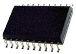
KEG SUFFIX (Pb-FREE)
20-LEAD SOIC
CASE 475A-02
ORDERING INFORMATION
Device
Temperature Range
Case No.
Package
MMA3221EG
–40 to +125°C
475A-02
SOIC-20
MMA3221EGR2
–40 to +125°C
475A-02
SOIC-20, Tape & Reel
MMA3221KEG*
–40 to +125°C
475A-02
SOIC-20
MMA3221KEGR2*
–40 to +125°C
475A-02
SOIC-20, Tape & Reel
*Part number sourced from a different facility.
AVDD
G-Cell
Sensor
ST
Self-Test
Integrator
Gain
Filter
Temp
VDD
N/C
1
20
GND
XOUT
N/C
2
19
N/C
N/C
3
18
N/C
N/C
4
17
N/C
ST
5
16
N/C
XOUT
6
15
N/C
STATUS
7
14
N/C
VSS
8
13
N/C
VDD
9
12
N/C
10
11
YOUT
YOUT
Control Logic &
EPROM
Trim Circuits
Oscillator
Clock
Gen.
Status
Figure 1. Simplified Accelerometer Functional Block Diagram
© 2011, 2012 Freescale Semiconductor, Inc. All rights reserved.
VSS
AVDD
Figure 2. Pin Connections
�Table 1. Maximum Ratings
(Maximum ratings are the limits to which the device can be exposed without causing permanent damage.)
Rating
Symbol
Value
Unit
Powered Acceleration (all axes)
Gpd
1500
g
Unpowered Acceleration (all axes)
Gupd
2000
g
Supply Voltage
VDD
–0.3 to +7.0
V
Drop Test (1)
Ddrop
1.2
m
Tstg
–40 to +125
°C
Storage Temperature Range
NOTES:
1. Dropped onto concrete surface from any axis.
ELECTRO STATIC DISCHARGE (ESD)
WARNING: This device is sensitive to electrostatic
discharge.
Although the Freescale accelerometers contain internal
2kV ESD protection circuitry, extra precaution must be taken
by the user to protect the chip from ESD. A charge of over
2000 volts can accumulate on the human body or associated
test equipment. A charge of this magnitude can alter the
performance or cause failure of the chip. When handling the
accelerometer, proper ESD precautions should be followed
to avoid exposing the device to discharges which may be
detrimental to its performance.
MMA3221KEG
2
Sensors
Freescale Semiconductor, Inc.
�Table 2. Operating Characteristics
(Unless otherwise noted: –40°C TA +105°C, 4.75 VDD 5.25, Acceleration = 0g, Loaded output.(1))
Characteristic
Symbol
Min
Typ
Max
Unit
VDD
IDD
TA
gFS
gFS
4.75
6
–40
—
—
5.00
8
—
112.5
33.75
5.25
10
+125
—
—
V
mA
°C
g
g
VOFF
VOFF
VOFF,V
VOFF,V
S
S
SV
SV
f–3dB
NLOUT
2.30
2.30
0.41 VDD
0.44 VDD
38
95
7.44
18.6
360
–1.0
2.5
2.5
0.50 VDD
0.50 VDD
40
100
8
20
400
—
2.70
2.70
0.56 VDD
0.56 VDD
42
105
8.56
21.4
440
+1.0
V
V
V
V
mV/g
mV/g
mV/g/V
mV/g/V
Hz
% FSO
nRMS
nPSD
nCLK
—
—
—
—
110
2.0
2.8
—
—
mVrms
V/(Hz1/2)
mVpk
Self-Test
Output Response(7)
Input Low
Input High
Input Loading(8)
Response Time(9)
gST
VIL
VIH
IIN
tST
9.6
VSS
0.7 VDD
–30
—
12
—
—
–100
2.0
14.4
0.3 VDD
VDD
–300
–
g
V
V
A
ms
Status(13)(14)
Output Low (Iload = 100 A)
Output High (Iload = 100 A)
VOL
VOH
—
VDD –0.8
—
—
0.4
—
V
V
Minimum Supply Voltage (LVD Trip)
VLVD
2.7
3.25
4.0
V
fmin
50
—
260
kHz
Output Stage Performance
Electrical Saturation Recovery Time(10)
Full Scale Output Range (IOUT = 200 A)
Capacitive Load Drive(11)
Output Impedance
tDELAY
VFSO
CL
ZO
—
0.25
—
—
0.2
—
—
300
—
VDD – 0.25
100
—
ms
V
pF
Mechanical Characteristics
Transverse Sensitivity(12)
Package Resonance
VXZ,YZ
fPKG
—
—
—
10
5.0
—
% FSO
kHz
(2)
(3)
Operating Range
Supply Voltage
Supply Current
Operating Temperature Range
Acceleration Range X-axis
Acceleration Range Y-axis
Output Signal
Zero g X-axis (TA = 25°C, VDD = 5.0 V)(4)
Zero g Y-axis (TA = 25°C, VDD = 5.0 V)(4)
Zero g X-axis
Zero g Y-axis
Sensitivity X-axis (TA = 25°C, VDD = 5.0 V)(5)
Sensitivity Y-axis (TA = 25°C, VDD = 5.0 V)(5)
Sensitivity X-axis
Sensitivity Y-axis
Bandwidth Response
Nonlinearity
Noise
RMS (.01 Hz – 1 kHz)
Power Spectral Density
Clock Noise (without RC load on output)(6)
Clock Monitor Fail Detection Frequency
NOTES:
1. For a loaded output the measurements are observed after an RC filter consisting of a 1 k resistor and a 0.01 F capacitor to ground.
2. These limits define the range of operation for which the part will meet specification.
3. Within the supply range of 4.75 and 5.25 volts, the device operates as a fully calibrated linear accelerometer. Beyond these supply limits
the device may operate as a linear device but is not guaranteed to be in calibration.
4. The device can measure both + and – acceleration. With no input acceleration the output is at mid-supply. For positive acceleration the
output will increase above VDD/2 and for negative acceleration the output will decrease below VDD/2.
5. The device is calibrated at 20g.
6. At clock frequency 70 kHz.
7. VOFF calculated with typical sensitivity.
8. The digital input pin has an internal pull-down current source to prevent inadvertent self test initiation due to external board level leakages.
9. Time for the output to reach 90% of its final value after a self-test is initiated.
10. Time for amplifiers to recover after an acceleration signal causing them to saturate.
11. Preserves phase margin (60°) to guarantee output amplifier stability.
12. A measure of the device's ability to reject an acceleration applied 90° from the true axis of sensitivity.
13. The Status pin output is not valid following power-up until at least one rising edge has been applied to the self-test pin. The Status pin is
high whenever the self-test input is high, as a means to check the connectivity of the self-test and Status pins in the application.
14. The Status pin output latches high if a Low Voltage Detection or Clock Frequency failure occurs, or the EPROM parity changes to odd. The
Status pin can be reset low if the self-test pin is pulsed with a high input for at least 100 s, unless a fault condition continues to exist.
MMA3221KEG
Sensors
Freescale Semiconductor, Inc.
3
�PRINCIPLE OF OPERATION
The Freescale accelerometer is a surface-micromachined
integrated-circuit accelerometer.
The device consists of a surface micromachined
capacitive sensing cell (g-cell) and a CMOS signal
conditioning ASIC contained in a single integrated circuit
package. The sensing element is sealed hermetically at the
wafer level using a bulk micromachined “cap'' wafer.
The g-cell is a mechanical structure formed from
semiconductor materials (polysilicon) using semiconductor
processes (masking and etching). It can be modeled as two
stationary plates with a moveable plate in-between. The
center plate can be deflected from its rest position by
subjecting the system to an acceleration (Figure 3).
When the center plate deflects, the distance from it to one
fixed plate will increase by the same amount that the distance
to the other plate decreases. The change in distance is a
measure of acceleration.
The g-cell plates form two back-to-back capacitors
(Figure 4). As the center plate moves with acceleration, the
distance between the plates changes and each capacitor's
value will change, (C = A/D). Where A is the area of the
plate, is the dielectric constant, and D is the distance
between the plates.
The CMOS ASIC uses switched capacitor techniques to
measure the g-cell capacitors and extract the acceleration
data from the difference between the two capacitors. The
ASIC also signal conditions and filters (switched capacitor)
the signal, providing a high level output voltage that is
ratiometric and proportional to acceleration.
Acceleration
Figure 3. Transducer
Physical Model
Figure 4. Equivalent
Circuit Model
SPECIAL FEATURES
Filtering
The Freescale accelerometers contain an onboard 2-pole
switched capacitor filter. A Bessel implementation is used
because it provides a maximally flat delay response (linear
phase) thus preserving pulse shape integrity. Because the
filter is realized using switched capacitor techniques, there is
no requirement for external passive components (resistors
and capacitors) to set the cut-off frequency.
Self-Test
The sensor provides a self-test feature that allows the
verification of the mechanical and electrical integrity of the
accelerometer at any time before or after installation. This
feature is critical in applications such as automotive airbag
systems where system integrity must be ensured over the life
of the vehicle. A fourth “plate'' is used in the g-cell as a selftest plate. When the user applies a logic high input to the selftest pin, a calibrated potential is applied across the self-test
plate and the moveable plate. The resulting electrostatic
2
1 V
force Fe = --- A ------ causes the center plate to deflect.
2 d2
The resultant deflection is measured by the accelerometer's
control ASIC and a proportional output voltage results. This
procedure assures that both the mechanical (g-cell) and
electronic sections of the accelerometer are functioning.
Status
Freescale accelerometers include fault detection circuitry
and a fault latch. The Status pin is an output from the fault
latch, OR'd with self-test, and is set high whenever the
following event occurs:
• Parity of the EPROM bits becomes odd in number.
The fault latch can be reset by a rising edge on the self-test
input pin, unless one (or more) of the fault conditions
continues to exist.
MMA3221KEG
4
Sensors
Freescale Semiconductor, Inc.
�BASIC CONNECTIONS
Pinout Description
PCB Layout
20
GND
N/C
2
19
N/C
N/C
3
18
N/C
N/C
4
17
N/C
ST
5
16
N/C
XOUT
6
15
N/C
STATUS
VSS
7
14
N/C
8
13
N/C
VDD
9
12
N/C
AVDD
11
10
P1
STATUS
Accelerometer
1
P0
ST
XOUT
A/D In
R
1 k C 0.01 F
YOUT
VSS
VDD
R
1 k
A/D In
C 0.01 F
Microcontroller
N/C
VSS
C
0.1 F
VDD
C 0.1 F
VRH
C 0.1 F
YOUT
Power Supply
Pin No.
Pin Name
Description
1 thru 3
—
Leave unconnected.
4
—
No internal connection. Leave
unconnected.
5
ST
Logic input pin used to initiate
self-test.
6
XOUT
Output voltage of the
accelerometer. X Direction.
7
STATUS
Logic output pin to indicate
fault.
8
VSS
The power supply ground.
9
VDD
The power supply input.
10
AVDD
Power supply input (Analog).
11
YOUT
Output voltage of the
accelerometer. Y Direction.
12 thru 16
—
Used for factory trim. Leave
unconnected.
17 thru 19
—
No internal connection. Leave
unconnected.
20
GND
Ground.
MMA3221KEG
VDD
Logic
Input
C1
0.1 F
5
ST
9
VDD
10
8
XOUT
AVDD
7
Status
R1
1 k
6
Figure 4. Recommended PCB Layout for Interfacing
Accelerometer to Microcontroller
NOTES:
• Use a 0.1 F capacitor on VDD to decouple the power
source.
• Physical coupling distance of the accelerometer to the
microcontroller should be minimal.
• Place a ground plane beneath the accelerometer to
reduce noise, the ground plane should be attached to all
of the open ended terminals shown in Figure 4.
• Use an RC filter of 1 k and 0.01 F on the output of the
accelerometer to minimize clock noise (from the switched
capacitor filter circuit).
• PCB layout of power and ground should not couple power
supply noise.
• Accelerometer and microcontroller should not be a high
current path.
• A/D sampling rate and any external power supply
switching frequency should be selected such that they do
not interfere with the internal accelerometer sampling
frequency. This will prevent aliasing errors.
X Output
Signal
C2
0.01 F
VSS
YOUT
11
R2
1 k
Y Output
Signal
C3
0.01 F
Figure 3. SOIC Accelerometer with Recommended
Connection Diagram
MMA3221KEG
Sensors
Freescale Semiconductor, Inc.
5
�Dynamic Acceleration Sensing Direction
Y
Acceleration of the
package in the X and
Y direction (center plates
move in the X and Y
direction) will result in an
increase in the X and Y
outputs.
X
N/C
1
20
GND
N/C
2
19
N/C
N/C
3
18
N/C
N/C
4
17
N/C
ST
5
16
N/C
XOUT
6
15
N/C
STATUS
7
14
N/C
VSS
8
13
N/C
VDD
9
12
N/C
AVDD
10
11
YOUT
X
Activation of Self test moves
the center plates in the X
and Y direction, resulting in
an increase in the X and Y
outputs.
Y
20-Pin SOIC Package
N/C pins are recommended to be left FLOATING
Top View
Static Acceleration Sensing Direction
10 9
8 7
6
5 4
3
2
1
Direction of Earth’s gravity field.*
11 12 13 14 15 16 17 18 19 20
Front View
Side View
* When positioned as shown, the Earth’s gravity will result in a positive 1g output in the X channel.
MMA3221KEG
6
Sensors
Freescale Semiconductor, Inc.
�MINIMUM RECOMMENDED FOOTPRINT FOR SURFACE MOUNTED APPLICATIONS
Surface mount board layout is a critical portion of the total
design. The footprint for the surface mount packages must be
the correct size to ensure proper solder connection interface
between the board and the package. With the correct
0.380 in.
9.65 mm
footprint, the packages will self-align when subjected to a
solder reflow process. It is always recommended to design
boards with a solder mask layer to avoid bridging and
shorting between solder pads.
0.050 in.
1.27 mm
0.024 in.
0.610 mm
0.080 in.
2.03 mm
Figure 5. Footprint SOIC-20 (Case 475A-02)
MMA3221KEG
Sensors
Freescale Semiconductor, Inc.
7
�PACKAGE DIMENSIONS
PAGE 1 OF 2
CASE 475A-02
ISSUE C
20-LEAD SOIC
MMA3221KEG
8
Sensors
Freescale Semiconductor, Inc.
�PACKAGE DIMENSIONS
PAGE 2 OF 2
CASE 475A-02
ISSUE C
20-LEAD SOIC
MMA3221KEG
Sensors
Freescale Semiconductor, Inc.
9
�Table 4. Revision History
Revision
number
Revision
date
1
11/2012
Description of changes
• Table 2. Operating Characteristics, added footnote for Self-Test Output Response, updated page
4: Principle of Operation
MMA3221KEG
Sensors
Freescale Semiconductor, Inc.
10
�How to Reach Us:
Information in this document is provided solely to enable system and software
implementers to use Freescale products. There are no express or implied copyright
Home Page:
freescale.com
Web Support:
freescale.com/support
licenses granted hereunder to design or fabricate any integrated circuits based on the
information in this document.
Freescale reserves the right to make changes without further notice to any products
herein. Freescale makes no warranty, representation, or guarantee regarding the
suitability of its products for any particular purpose, nor does Freescale assume any
liability arising out of the application or use of any product or circuit, and specifically
disclaims any and all liability, including without limitation consequential or incidental
damages. “Typical” parameters that may be provided in Freescale data sheets and/or
specifications can and do vary in different applications, and actual performance may
vary over time. All operating parameters, including “typicals,” must be validated for each
customer application by customer’s technical experts. Freescale does not convey any
license under its patent rights nor the rights of others. Freescale sells products pursuant
to standard terms and conditions of sale, which can be found at the following address:
freescale.com/salestermsandconditions.
Freescale, the Freescale logo, Energy Efficient Solutions logo, are trademarks of
Freescale Semiconductor, Inc., Reg. U.S. Pat. & Tm. Off. Xtrinsic is a trademark of
Freescale Semiconductor, Inc. All other product or service names are the property of
their respective owners.
© 2012 Freescale Semiconductor, Inc.
MMA3221KEG
Rev. 1
11/2012
�


 工商网监
湘ICP备2023018690号
工商网监
湘ICP备2023018690号
