Freescale Semiconductor
Document Number: MPC755EC
Rev. 8, 02/2006
Technical Data
MPC755
RISC Microprocessor
Hardware Specifications
This document is primarily concerned with the MPC755;
however, unless otherwise noted, all information here also
applies to the MPC745. The MPC755 and MPC745 are
reduced instruction set computing (RISC) microprocessors
that implement the PowerPC™ instruction set architecture.
This document describes pertinent physical characteristics of
the MPC755. For information on specific MPC755 part
numbers covered by this or other specifications, see
Section 10, “Ordering Information.” For functional
characteristics of the processor, refer to the MPC750 RISC
Microprocessor Family User’s Manual.
To locate any published errata or updates for this document,
refer to the website listed on the back cover of this document.
1
Overview
The MPC755 is targeted for low-cost, low-power systems
and supports the following power management
features—doze, nap, sleep, and dynamic power
management. The MPC755 consists of a processor core and
an internal L2 tag combined with a dedicated L2 cache
interface and a 60x bus. The MPC745 is identical to the
MPC755 except it does not support the L2 cache interface.
Figure 1 shows a block diagram of the MPC755.
© Freescale Semiconductor, Inc., 2006. All rights reserved.
1.
2.
3.
4.
5.
6.
7.
8.
9.
10.
Contents
Overview . . . . . . . . . . . . . . . . . . . . . . . . . . . . . . . . . . . 1
Features . . . . . . . . . . . . . . . . . . . . . . . . . . . . . . . . . . . . 3
General Parameters . . . . . . . . . . . . . . . . . . . . . . . . . . . 5
Electrical and Thermal Characteristics . . . . . . . . . . . . 6
Pin Assignments . . . . . . . . . . . . . . . . . . . . . . . . . . . . 25
Pinout Listings . . . . . . . . . . . . . . . . . . . . . . . . . . . . . 27
Package Description . . . . . . . . . . . . . . . . . . . . . . . . . 32
System Design Information . . . . . . . . . . . . . . . . . . . 36
Document Revision History . . . . . . . . . . . . . . . . . . . 50
Ordering Information . . . . . . . . . . . . . . . . . . . . . . . . 53
�2
Integer Unit 2
+
Integer Unit 1
+ × ÷
Reorder Buffer
(6-Entry)
Completion Unit
32-Bit
Reservation
Station
Reservation
Station
2 Instructions
• Time Base Counter/Decrementer
• Clock Multiplier
• JTAG/COP Interface
• Thermal/Power Management
• Performance Monitor
Additional Features
DTLB
SRs
(Original)
DBAT
Array
Data MMU
32-Bit
CR
System Register
Unit
Reservation
Station
Tags
PA
32-Kbyte
D Cache
17-Bit L2 Address Bus
64-Bit L2 Data Bus
Data Load Queue
L1 Castout Queue
Instruction Fetch Queue
32-Kbyte
I Cache
Reservation Station
Tags
L2CR
L2 Tags
Not in the MPC745
L2 Castout Queue
L2 Controller
FPSCR
FPSCR
+ × ÷
64-Bit Floating-Point
Unit
IBAT
Array
128-Bit
(4 Instructions)
L2 Bus Interface
Unit
Rename Buffers
(6)
FPR File
ITLB
SRs
(Shadow)
Instruction MMU
60x Bus Interface Unit
Store Queue
(EA Calculation)
+
Load/Store Unit 64-Bit
64-Bit
32-Bit
Reservation Station
(2-Entry)
32-Bit Address Bus
32-/64-Bit Data Bus
EA
CTR
LR
64-Bit
(2 Instructions)
BHT
BTIC
64-Entry
Branch Processing
Unit
Rename Buffers
(6)
GPR File
Dispatch Unit
Instruction Queue
(6-Word)
Fetcher
Instruction Unit
Overview
Figure 1. MPC755 Block Diagram
MPC755 RISC Microprocessor Hardware Specifications, Rev. 8
Freescale Semiconductor
�Features
2
Features
This section summarizes features of the MPC755 implementation of the PowerPC architecture. Major
features of the MPC755 are as follows:
• Branch processing unit
— Four instructions fetched per clock
— One branch processed per cycle (plus resolving two speculations)
— Up to one speculative stream in execution, one additional speculative stream in fetch
— 512-entry branch history table (BHT) for dynamic prediction
— 64-entry, four-way set-associative branch target instruction cache (BTIC) for eliminating
branch delay slots
• Dispatch unit
— Full hardware detection of dependencies (resolved in the execution units)
— Dispatch two instructions to six independent units (system, branch, load/store, fixed-point
unit 1, fixed-point unit 2, floating-point)
— Serialization control (predispatch, postdispatch, execution serialization)
• Decode
— Register file access
— Forwarding control
— Partial instruction decode
• Completion
— Six-entry completion buffer
— Instruction tracking and peak completion of two instructions per cycle
— Completion of instructions in program order while supporting out-of-order instruction
execution, completion serialization, and all instruction flow changes
• Fixed point units (FXUs) that share 32 GPRs for integer operands
— Fixed Point Unit 1 (FXU1)—multiply, divide, shift, rotate, arithmetic, logical
— Fixed Point Unit 2 (FXU2)—shift, rotate, arithmetic, logical
— Single-cycle arithmetic, shifts, rotates, logical
— Multiply and divide support (multi-cycle)
— Early out multiply
• Floating-point unit and a 32-entry FPR file
— Support for IEEE standard 754 single- and double-precision floating-point arithmetic
— Hardware support for divide
— Hardware support for denormalized numbers
— Single-entry reservation station
— Supports non-IEEE mode for time-critical operations
— Three-cycle latency, one-cycle throughput, single-precision multiply-add
MPC755 RISC Microprocessor Hardware Specifications, Rev. 8
Freescale Semiconductor
3
�Features
•
•
•
•
— Three-cycle latency, one-cycle throughput, double-precision add
— Four-cycle latency, two-cycle throughput, double-precision multiply-add
System unit
— Executes CR logical instructions and miscellaneous system instructions
— Special register transfer instructions
Load/store unit
— One-cycle load or store cache access (byte, half-word, word, double word)
— Effective address generation
— Hits under misses (one outstanding miss)
— Single-cycle unaligned access within double-word boundary
— Alignment, zero padding, sign extend for integer register file
— Floating-point internal format conversion (alignment, normalization)
— Sequencing for load/store multiples and string operations
— Store gathering
— Cache and TLB instructions
— Big- and little-endian byte addressing supported
Level 1 cache structure
— 32K, 32-byte line, eight-way set-associative instruction cache (iL1)
— 32K, 32-byte line, eight-way set-associative data cache (dL1)
— Cache locking for both instruction and data caches, selectable by group of ways
— Single-cycle cache access
— Pseudo least-recently-used (PLRU) replacement
— Copy-back or write-through data cache (on a page per page basis)
— MEI data cache coherency maintained in hardware
— Nonblocking instruction and data cache (one outstanding miss under hits)
— No snooping of instruction cache
Level 2 (L2) cache interface (not implemented on MPC745)
— Internal L2 cache controller and tags; external data SRAMs
— 256K, 512K, and 1 Mbyte two-way set-associative L2 cache support
— Copy-back or write-through data cache (on a page basis, or for all L2)
— Instruction-only mode and data-only mode
— 64-byte (256K/512K) or 128-byte (1M) sectored line size
— Supports flow through (register-buffer) synchronous BurstRAMs, pipelined (register-register)
synchronous BurstRAMs (3-1-1-1 or strobeless 4-1-1-1) and pipelined (register-register) late
write synchronous BurstRAMs
— L2 configurable to cache, private memory, or split cache/private memory
— Core-to-L2 frequency divisors of ÷1, ÷1.5, ÷2, ÷2.5, and ÷3 supported
— 64-bit data bus
MPC755 RISC Microprocessor Hardware Specifications, Rev. 8
4
Freescale Semiconductor
�General Parameters
•
•
•
•
•
3
— Selectable interface voltages of 2.5 and 3.3 V
— Parity checking on both L2 address and data
Memory management unit
— 128-entry, two-way set-associative instruction TLB
— 128-entry, two-way set-associative data TLB
— Hardware reload for TLBs
— Hardware or optional software tablewalk support
— Eight instruction BATs and eight data BATs
— Eight SPRGs, for assistance with software tablewalks
— Virtual memory support for up to 4 exabytes (252) of virtual memory
— Real memory support for up to 4 gigabytes (232) of physical memory
Bus interface
— Compatible with 60x processor interface
— 32-bit address bus
— 64-bit data bus, 32-bit mode selectable
— Bus-to-core frequency multipliers of 2x, 3x, 3.5x, 4x, 4.5x, 5x, 5.5x, 6x, 6.5x, 7x, 7.5x, 8x, 10x
supported
— Selectable interface voltages of 2.5 and 3.3 V
— Parity checking on both address and data buses
Power management
— Low-power design with thermal requirements very similar to MPC740/MPC750
— Three static power saving modes: doze, nap, and sleep
— Dynamic power management
Integrated thermal management assist unit
— On-chip thermal sensor and control logic
— Thermal management interrupt for software regulation of junction temperature
Testability
— LSSD scan design
— IEEE 1149.1 JTAG interface
General Parameters
The following list provides a summary of the general parameters of the MPC755:
Technology
0.22 µm CMOS, six-layer metal
Die size
6.61 mm × 7.73 mm (51 mm2)
Transistor count
6.75 million
Logic design
Fully-static
MPC755 RISC Microprocessor Hardware Specifications, Rev. 8
Freescale Semiconductor
5
�Electrical and Thermal Characteristics
Packages
Core power supply
I/O power supply
4
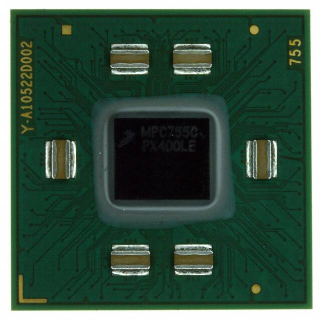
MPC745: Surface mount 255 plastic ball grid array (PBGA)
MPC755: Surface mount 360 ceramic ball grid array (CBGA)
Surface mount 360 plastic ball grid array (PBGA)
2.0 V ± 100 mV DC (nominal; some parts support core voltages down to
1.8 V; see Table 3 for recommended operating conditions)
2.5 V ± 100 mV DC or
3.3 V ± 165 mV DC (input thresholds are configuration pin selectable)
Electrical and Thermal Characteristics
This section provides the AC and DC electrical specifications and thermal characteristics for the MPC755.
4.1
DC Electrical Characteristics
Table 1 through Table 7 describe the MPC755 DC electrical characteristics. Table 1 provides the absolute
maximum ratings.
Table 1. Absolute Maximum Ratings1
Characteristic
Symbol
Maximum Value
Unit
Notes
Core supply voltage
VDD
–0.3 to 2.5
V
4
PLL supply voltage
AVDD
–0.3 to 2.5
V
4
L2AVDD
–0.3 to 2.5
V
4
OVDD
–0.3 to 3.6
V
3
L2OVDD
–0.3 to 3.6
V
3
Processor bus
Vin
–0.3 to OVDD + 0.3 V
V
2, 5
L2 bus
Vin
–0.3 to L2OVDD + 0.3 V
V
2, 5
JTAG signals
Vin
–0.3 to 3.6
V
Tstg
–55 to 150
°C
L2 DLL supply voltage
Processor bus supply voltage
L2 bus supply voltage
Input voltage
Storage temperature range
Notes:
1. Functional and tested operating conditions are given in Table 3. Absolute maximum ratings are stress ratings only, and
functional operation at the maximums is not guaranteed. Stresses beyond those listed may affect device reliability or cause
permanent damage to the device.
2. Caution: Vin must not exceed OVDD or L2OVDD by more than 0.3 V at any time including during power-on reset.
3. Caution: L2OVDD/OVDD must not exceed VDD/AVDD/L2AVDD by more than 1.6 V during normal operation. During power-on
reset and power-down sequences, L2OVDD/OVDD may exceed VDD/AVDD/L2AVDD by up to 3.3 V for up to 20 ms, or by 2.5 V
for up to 40 ms. Excursions beyond 3.3 V or 40 ms are not supported.
4. Caution: VDD/AVDD/L2AVDD must not exceed L2OVDD/OVDD by more than 0.4 V during normal operation. During power-on
reset and power-down sequences, VDD/AVDD/L2AVDD may exceed L2OVDD/OVDD by up to 1.0 V for up to 20 ms, or by 0.7 V
for up to 40 ms. Excursions beyond 1.0 V or 40 ms are not supported.
5. This is a DC specifications only. Vin may overshoot/undershoot to a voltage and for a maximum duration as shown in Figure 2.
MPC755 RISC Microprocessor Hardware Specifications, Rev. 8
6
Freescale Semiconductor
�Electrical and Thermal Characteristics
Figure 2 shows the allowable undershoot and overshoot voltage on the MPC755.
(L2)OVDD + 20%
(L2)OVDD + 5%
(L2)OVDD
VIH
VIL
GND
GND – 0.3 V
GND – 0.7 V
Not to Exceed 10%
of tSYSCLK
Figure 2. Overshoot/Undershoot Voltage
The MPC755 provides several I/O voltages to support both compatibility with existing systems and
migration to future systems. The MPC755 core voltage must always be provided at nominal 2.0 V (see
Table 3 for actual recommended core voltage). Voltage to the L2 I/Os and processor interface I/Os are
provided through separate sets of supply pins and may be provided at the voltages shown in Table 2. The
input voltage threshold for each bus is selected by sampling the state of the voltage select pins BVSEL and
L2VSEL during operation. These signals must remain stable during part operation and cannot change. The
output voltage will swing from GND to the maximum voltage applied to the OVDD or L2OVDD power
pins.
Table 2 describes the input threshold voltage setting.
Table 2. Input Threshold Voltage Setting
Part
Revision
BVSEL Signal
Processor Bus
Interface Voltage
L2VSEL Signal
L2 Bus
Interface Voltage
E
0
Not Available
0
Not Available
1
2.5 V/3.3 V
1
2.5 V/3.3 V
Caution: The input threshold selection must agree with the OVDD/L2OVDD voltages supplied.
Note: The input threshold settings above are different for all revisions prior to Rev. 2.8 (Rev. E). For more information,
refer to Section 10.2, “Part Numbers Not Fully Addressed by This Document.”
MPC755 RISC Microprocessor Hardware Specifications, Rev. 8
Freescale Semiconductor
7
�Electrical and Thermal Characteristics
Table 3 provides the recommended operating conditions for the MPC755.
Table 3. Recommended Operating Conditions 1
Recommended Value
Characteristic
Symbol
300 MHz, 350 MHz
400 MHz
Min
Max
Min
Max
Unit
Notes
Core supply voltage
VDD
1.80
2.10
1.90
2.10
V
3
PLL supply voltage
AVDD
1.80
2.10
1.90
2.10
V
3
L2AVDD
1.80
2.10
1.90
2.10
V
3
OVDD
2.375
2.625
2.375
2.625
V
2, 4
3.135
3.465
3.135
3.465
2.375
2.625
2.375
2.625
3.135
3.465
3.135
3.465
L2 DLL supply voltage
Processor bus supply
voltage
BVSEL = 1
L2 bus supply voltage
L2VSEL = 1
Input voltage
Die-junction temperature
L2OVDD
5
V
2, 4
5
Processor bus
Vin
GND
OVDD
GND
OVDD
V
L2 bus
Vin
GND
L2OVDD
GND
L2OVDD
V
JTAG signals
Vin
GND
OVDD
GND
OVDD
V
Tj
0
105
0
105
°C
Notes:
1. These are the recommended and tested operating conditions. Proper device operation outside of these conditions is not
guaranteed.
2. Revisions prior to Rev. 2.8 (Rev. E) offered different I/O voltage support. For more information, refer to Section 10.2, “Part
Numbers Not Fully Addressed by This Document.”
3. 2.0 V nominal.
4. 2.5 V nominal.
5. 3.3 V nominal.
Table 4 provides the package thermal characteristics for the MPC755 and MPC745. The MPC755 was
initially sampled in a CBGA package, but production units are currently provided in both a CBGA and a
PBGA package. Because of the better long-term device-to-board interconnect reliability of the PBGA
package, Freescale recommends use of a PBGA package except where circumstances dictate use of a
CBGA package. The MPC745 is offered in a PBGA package only.
MPC755 RISC Microprocessor Hardware Specifications, Rev. 8
8
Freescale Semiconductor
�Electrical and Thermal Characteristics
Table 4. Package Thermal Characteristics 6
Value
Characteristic
Symbol
MPC755
CBGA
MPC755
PBGA
MPC745
PBGA
Unit
Notes
Junction-to-ambient thermal resistance, natural
convection
RθJA
24
31
34
°C/W
1, 2
Junction-to-ambient thermal resistance, natural
convection, four-layer (2s2p) board
RθJMA
17
25
26
°C/W
1, 3
Junction-to-ambient thermal resistance, 200 ft/min
airflow, single-layer (1s) board
RθJMA
18
25
27
°C/W
1, 3
Junction-to-ambient thermal resistance, 200 ft/min
airflow, four-layer (2s2p) board
RθJMA
14
21
22
°C/W
1, 3
Junction-to-board thermal resistance
RθJB
8
17
17
°C/W
4
Junction-to-case thermal resistance
RθJC