Freescale Semiconductor
Document Number: MPC8308EC
Rev. 4, 12/2014
MPC8308 PowerQUICC II Pro
Processor Hardware Specification
This document provides an overview of the MPC8308
features and its hardware specifications, including a block
diagram showing the major functional components. The
MPC8308 is a cost-effective, low-power, highly integrated
host processor. The MPC8308 extends the PowerQUICC
family, adding higher CPU performance, additional
functionality, and faster interfaces while addressing the
requirements related to time-to-market, price, power
consumption, and package size.
© Freescale Semiconductor, Inc., 2011, 2014. All rights reserved.
1.
2.
3.
4.
5.
6.
7.
8.
9.
10.
11.
12.
13.
14.
15.
16.
17.
18.
19.
20.
21.
22.
23.
24.
25.
Contents
Overview . . . . . . . . . . . . . . . . . . . . . . . . . . . . . . . . . . . 2
Electrical Characteristics . . . . . . . . . . . . . . . . . . . . . . 2
Power characteristics . . . . . . . . . . . . . . . . . . . . . . . . . 6
Clock input timing . . . . . . . . . . . . . . . . . . . . . . . . . . . 7
RESET initialization . . . . . . . . . . . . . . . . . . . . . . . . . . 8
DDR2 SDRAM . . . . . . . . . . . . . . . . . . . . . . . . . . . . . 10
DUART . . . . . . . . . . . . . . . . . . . . . . . . . . . . . . . . . . . 14
Ethernet: Three-Speed Ethernet, MII management . 15
USB . . . . . . . . . . . . . . . . . . . . . . . . . . . . . . . . . . . . . . 23
High-Speed Serial interfaces (HSSI) . . . . . . . . . . . . 25
PCI Express . . . . . . . . . . . . . . . . . . . . . . . . . . . . . . . . 34
Enhanced Local Bus . . . . . . . . . . . . . . . . . . . . . . . . . 41
Enhanced Secure Digital Host Controller (eSDHC) . 44
JTAG . . . . . . . . . . . . . . . . . . . . . . . . . . . . . . . . . . . . . 50
I2C . . . . . . . . . . . . . . . . . . . . . . . . . . . . . . . . . . . . . . . 53
Timers . . . . . . . . . . . . . . . . . . . . . . . . . . . . . . . . . . . . 55
GPIO . . . . . . . . . . . . . . . . . . . . . . . . . . . . . . . . . . . . . 56
IPIC . . . . . . . . . . . . . . . . . . . . . . . . . . . . . . . . . . . . . . 57
SPI . . . . . . . . . . . . . . . . . . . . . . . . . . . . . . . . . . . . . . . 57
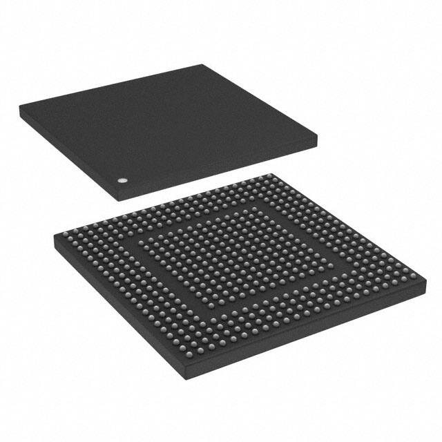
Package and Pin Listings . . . . . . . . . . . . . . . . . . . . . 59
Clocking . . . . . . . . . . . . . . . . . . . . . . . . . . . . . . . . . . 71
Thermal . . . . . . . . . . . . . . . . . . . . . . . . . . . . . . . . . . . 74
System Design Information . . . . . . . . . . . . . . . . . . . 77
Ordering Information . . . . . . . . . . . . . . . . . . . . . . . . 80
Revision history . . . . . . . . . . . . . . . . . . . . . . . . . . . . 82
�Overview
1
Overview
This figure shows the major functional units within the MPC8308. The e300 core in the MPC8308, with
its 16 Kbytes of instruction and 16 Kbytes of data cache, implements the Power Architecture user
instruction set architecture and provides hardware and software debugging support. In addition, the
MPC8308 offers a PCI Express controller, two three-speed 10, 100, 1000 Mbps Ethernet controllers
(eTSEC), a DDR2 SDRAM memory controller, a SerDes block, an enhanced local bus controller (eLBC),
an integrated programmable interrupt controller (IPIC), a general purpose DMA controller, two I2C
controllers, dual UART (DUART), GPIOs, USB, general purpose timers, and an SPI controller. The high
level of integration in the MPC8308 helps simplify board design and offers significant bandwidth and
performance.
This figure shows a block diagram of the device.
e300c3 Core with
Power Management
DUART
I2C
Timers
GPIO, SPI
Enhanced
Secure
Digital Host
Controller
16-Kbyte
I-Cache
Interrupt
Controller
16-Kbyte
D-Cache
FPU
DMA
USB 2.0 HS
Host/Device/OTG
PCI
Express
x1
ULPI
Enhanced
Local Bus
DDR2
Controller
eTSEC1
eTSEC2
RGMII,MII
RGMII,MII
Figure 1. MPC8308 Block Diagram
2
Electrical Characteristics
This section provides the AC and DC electrical specifications and thermal characteristics for the
MPC8308. The device is currently targeted to these specifications. Some of these specifications are
independent of the I/O cell, but are included for a more complete reference. These are not purely I/O buffer
design specifications.
2.1
Overall DC Electrical Characteristics
This section covers the ratings, conditions, and other characteristics.
MPC8308 PowerQUICC II Pro Processor Hardware Specification, Rev. 4
2
Freescale Semiconductor
�Electrical Characteristics
2.1.1
Absolute maximum ratings
This table lists the absolute maximum ratings.
Table 1. Absolute maximum ratings1
Characteristic
Symbol
Max Value
Unit
Notes
Core supply voltage
VDD
–0.3 to 1.26
V
—
PLL supply voltage
AVDD1, AVDD2
–0.3 to 1.26
V
—
DDR2 DRAM I/O voltage
GVDD
–0.3 to 1.9
V
—
Local bus, DUART, system control and power management,
eSDHC, I2C, USB, Interrupt, Ethernet management, SPI,
Miscellaneous and JTAG I/O voltage
NVDD
–0.3 to 3.6
V
7
SerDes PHY
XCOREVDD,
XPADVDD,
SDAVDD
–0.3 to 1.26
V
—
eTSEC I/O Voltage
LVDD1, LVDD2
–0.3 to 2.75 or
–0.3 to 3.6
V
6, 8
MVIN
–0.3 to (GVDD + 0.3)
V
2, 5
MVREF
–0.3 to (GVDD + 0.3)
V
2, 5
eTSEC
LVIN
–0.3 to (LVDD + 0.3)
V
4, 5,8
Local bus, DUART, system control and power
management, eSDHC, I2C, Interrupt,
Ethernet management, SPI, Miscellaneous
and JTAG I/O voltage
OVIN
–0.3 to (NVDD + 0.3)
V
3, 5,7
TSTG
–55 to 150
C
—
Input voltage
DDR2 DRAM signals
DDR2 DRAM reference
Storage temperature range
Notes:
1. Functional and tested operating conditions are given in Table 2. Absolute maximum ratings are stress ratings only, and
functional operation at the maximums is not guaranteed. Stresses beyond those listed may affect device reliability or cause
permanent damage to the device.
2. Caution: MVIN must not exceed GVDD by more than 0.3 V. This limit may be exceeded for a maximum of 20 ms during
power-on reset and power-down sequences.
3. Caution: OVIN must not exceed NVDD by more than 0.3 V. This limit may be exceeded for a maximum of 20 ms during
power-on reset and power-down sequences.
4. Caution: LVIN must not exceed LVDD by more than 0.3 V. This limit may be exceeded for a maximum of 20 ms during
power-on reset and power-down sequences.
5. (M, L, O)VIN and MVREF may overshoot/undershoot to a voltage and for a maximum duration as shown in Figure 2
6. The max value of supply voltage should be selected based on the RGMII mode. The lower range applies to RGMII mode.
7. NVDD here refers to NVDDA, NVDDB,NVDDG, NVDDH, NVDDJ, NVDDP_K from the ball map.
8. LVDD1 here refers to NVDDC and LVDD2 refers to NVDDF from the ball map
2.1.2
Power supply voltage specification
This table provides the recommended operating conditions for the device. Note that the values in this table
are the recommended and tested operating conditions. Proper device operation outside of these conditions
is not guaranteed.
MPC8308 PowerQUICC II Pro Processor Hardware Specification, Rev. 4
Freescale Semiconductor
3
�Electrical Characteristics
Table 2. Recommended operating conditions
Symbol
Recommended Value1
Unit
SerDes internal digital power
XCOREVDD
1.0 V ± 50 mV
V
SerDes internal digital power
XCOREVSS
0.0
V
SerDes I/O digital power
XPADVDD
1.0 V ± 50 mV
V
SerDes analog power for PLL
SDAVDD
1.0 V ± 50 mV
V
SerDes analog power for PLL
SDAVSS
0
V
SerDes I/O digital power
XPADVSS
0
V
VDD
1.0 V ± 50 mV
V
Analog supply for e300 core APLL2
AVDD1
1.0 V ± 50 mV
V
Analog supply for system APLL2
AVDD2
1.0 V ± 50 mV
V
DDR2 DRAM I/O voltage
GVDD
1.8 V ± 100 mV
V
Differential reference voltage for DDR controller
MVREF
GVDD/2 (0.49 GVDD to
0.51 GVDD)
V
Standard I/O voltage (Local bus, DUART, system control and power
management, eSDHC, USB, I2C, Interrupt, Ethernet management,
SPI, Miscellaneous and JTAG I/O voltage)3
NVDD
3.3 V ± 300 mV
V
LVDD1, LVDD2
2.5 V ± 125 mV
3.3 V ± 300 mV
V
VSS
0.0
V
TA/TJ
Standard = 0 to 105
Extended = -40 to 105
C
Characteristic
Core supply voltage
eTSEC IO supply4,5
Analog and digital ground
Operating temperature range6
Notes:
1
2
3
4
5
6
GVDD, NVDD, AVDD, and VDD must track each other and must vary in the same direction—either in the positive or negative
direction.
This voltage is the input to the filter discussed in Section 23.2, “PLL Power Supply Filtering,” and not necessarily the voltage
at the AVDD pin, which may be reduced from VDD by the filter.
NVDD here refers to NVDDA, NVDDB,NVDDG, NVDDH, NVDDJ and NVDDP_K from the ball map.
The max value of supply voltage should be selected based on the RGMII mode. The lower range applies to RGMII mode.
LVDD1 here refers to NVDDC and LVDD2 refers to NVDDF from the ball map.
Minimum temperature is specified with TA; Maximum temperature is specified with TJ.
MPC8308 PowerQUICC II Pro Processor Hardware Specification, Rev. 4
4
Freescale Semiconductor
�Electrical Characteristics
This figure shows the undershoot and overshoot voltages at the interfaces of the device.
G/L/NVDD + 20%
G/L/NVDD + 5%
G/L/NVDD
VIH
VSS
VSS – 0.3 V
VIL
VSS – 0.7 V
Not to Exceed 10%
of tinterface1
Note:
1. tinterface refers to the clock period associated with the bus clock interface.
Figure 2. Overshoot/Undershoot Voltage for GVDD/NVDD/LVDD
2.1.3
Output driver characteristics
This table provides information on the characteristics of the output driver strengths.
Table 3. Output Drive Capability
Driver Type
Output Impedance ()
Supply Voltage
42
NVDD = 3.3 V
18
GVDD = 1.8 V
DUART, system control, I2C, JTAG, eSDHC, GPIO,SPI, USB
42
NVDD = 3.3 V
eTSEC signals
42
LVDD = 2.5/3.3 V
Local bus interface utilities signals
DDR2
1
2.1.4
signals1
Output Impedance can also be adjusted through configurable options in DDR Control Driver Register (DDRCDR).
For more information, see the MPC8308 PowerQUICC II Pro Processor Reference Manual.
Power sequencing
It is required to apply the core supply voltage (VDD) before the I/O supply voltages (GVDD, LVDD, and
NVDD) and assert PORESET before the power supplies fully ramp up. The core voltage supply must rise
to 90% of its nominal value before the I/O supplies reach 0.7 V; see Figure 3.
If this recommendation is not observed and I/O voltages are supplied before the core voltage, there might
be a period of time that all input and output pins are actively driven and cause contention and excessive
current. To overcome side effects of this condition, the application environment may require tuning of
external pull-up or pull-down resistors on particular signals to lesser values.
MPC8308 PowerQUICC II Pro Processor Hardware Specification, Rev. 4
Freescale Semiconductor
5
�Power characteristics
The I/O power supply ramp-up slew rate should be slower than 4V/100 s, this requirement is for ESD
circuit. Note that there is no specific power down sequence requirement for the device. I/O voltage
supplies (GVDD, LVDD, and NVDD) do not have any ordering requirements with respect to one another.
I/O Voltage (GVDD, LVDD, and NVDD)
V
Core Voltage (VDD)
0.7 V
90%
t
0
PORESET
>= 32 tSYS_CLK_IN
Figure 3. Power-Up sequencing example
3
Power characteristics
The estimated typical power dissipation, not including I/O supply power for the device is shown in this
table. Table 5 shows the estimated typical I/O power dissipation.
Table 4. MPC8308 power dissipation1
Core Frequency (MHz)
CSB Frequency (MHz)
Typical2
Maximum 3
Unit
266
133
530
900
mW
333
133
565
950
mW
400
133
600
1000
mW
Note:
1
The values do not include I/O supply power but do include core (VDD) and PLL (AVDD1,
AVDD2, XCOREVDD, XPADVDD, and SDAVDD)
2 Typical power is based on best process, a voltage of V
DD = 1.0 V and ambient temperature
of TA = 25 C and an artificial smoker test.
3 Maximum power is estimated based on best process, a voltage of V
DD = 1.05 V, a junction
temperature of TJ = 105 C
MPC8308 PowerQUICC II Pro Processor Hardware Specification, Rev. 4
6
Freescale Semiconductor
�Clock input timing
This table describes a typical scenario where blocks with the stated percentage of utilization and
impedances consume the amount of power described.
1
Table 5. MPC8308 typical I/O power dissipation
GVDD
(1.8 V)
NVDD
(3.3 V)
LVDD/
(3.3 V)
LVDD
(2.5 V)
Unit
Comments
250 MHz
32 bits+ECC
266 MHz
32 bits+ECC
0.302
—
—
—
W
—
62.5 MHz
66 MHZ
—
0.038
0.040
—
—
W
—
MII, 25 MHz
—
—
0.008
—
W
2 controllers
RGMII, 125 MHz
—
—
0.078
0.044
W
eSDHC IO Load = 40 pF
50 MHz
—
—
0.008
—
W
—
USB IO Load = 20 pF
60 MHz
—
—
0.012
W
—
—
—
0.017
—
W
—
Interface
Parameter
DDR2
Rs = 22
Rt = 75
Local bus I/O load = 20 pF
TSEC I/O load = 20 pF
Other I/O
4
0.309
—
Clock input timing
This section provides the clock input DC and AC electrical characteristics for the device.
4.1
DC electrical characteristics
This table provides the system clock input (SYS_CLK_IN) DC electrical specifications for the device.
Table 6. SYS_CLK_IN DC Electrical Characteristics
Parameter
Condition
Symbol
Min
Max
Unit
Input high voltage
—
VIH
2.4
NVDD + 0.3
V
Input low voltage
—
VIL
–0.3
0.4
V
0 V VIN NVDD
IIN
—
±10
A
SYS_CLK_IN input current
This table provides the RTC clock input (RTC_PIT_CLOCK) DC electrical specifications for the device.
Table 7. RTC_PIT_CLOCK DC Electrical Characteristics
Parameter
4.2
Condition
Symbol
Min
Input high voltage
—
VIH
3.3 V – 400 mV
Input low voltage
—
VIL
0
Max
Unit
V
0.4
V
AC electrical characteristics
The primary clock source for the device is SYS_CLK_IN. This table provides the system clock input
(SYS_CLK_IN) AC timing specifications for the device.
MPC8308 PowerQUICC II Pro Processor Hardware Specification, Rev. 4
Freescale Semiconductor
7
�RESET initialization
Table 8. SYS_CLK_IN AC Timing Specifications
Parameter/
Symbol
Min
Typ
Max
Unit
Notes
SYS_CLK_IN frequency
fSYS_CLK_IN
24
—
66.67
MHz
1, 6
SYS_CLK_IN period
tSYS_CLK_IN
15
—
41.67
ns
—
tKH, tKL
0.6
1.2
ns
2
tKHK/tSYS_CLK_IN
40
—
60
%
3
—
—
—
±150
ps
4, 5
SYS_CLK_IN rise and fall time
SYS_CLK_IN duty cycle
SYS_CLK_IN jitter
Notes:
1. Caution: The system and core must not exceed their respective maximum or minimum operating frequencies.
2. Rise and fall times for SYS_CLK_IN are measured at 0.4 and 2.7 V.
3. Timing is guaranteed by design and characterization.
4. This represents the total input jitter—short term and long term—and is guaranteed by design.
5. The SYS_CLK_IN driver’s closed loop jitter bandwidth should be 1,000,000
baud
1
16
—
2
Oversample rate
Notes:
1. Actual attainable baud rate is limited by the latency of interrupt processing.
2. The middle of a start bit is detected as the 8th sampled 0 after the 1-to-0 transition of the start bit.
Subsequent bit values are sampled each 16th sample.
8
Ethernet: Three-Speed Ethernet, MII management
This section provides the AC and DC electrical characteristics for three-speed, 10/100/1000, and MII
management. MPC8308 supports dual Ethernet controllers.
8.1
Enhanced Three-Speed Ethernet Controller (eTSEC)
(10/100/1000 Mbps)—MII/RGMII electrical characteristics
The electrical characteristics specified here apply to all the media independent interface (MII) and reduced
gigabit media independent interface (RGMII), signals except management data input/output (MDIO) and
management data clock (MDC). The RGMII interface is defined for 2.5 V, while the MII interface can be
operated at 3.3 V. The RGMII interface follows the Hewlett-Packard reduced pin-count interface for
Gigabit Ethernet Physical Layer Device Specification Version 1.2a (9/22/2000). The electrical
characteristics for MDIO and MDC are specified in Section 8.3, “Ethernet Management interface
electrical characteristics.”
MPC8308 PowerQUICC II Pro Processor Hardware Specification, Rev. 4
Freescale Semiconductor
15
�Ethernet: Three-Speed Ethernet, MII management
8.1.1
eTSEC DC electrical characteristics
All MII and RGMII drivers and receivers comply with the DC parametric attributes specified in Table 21
and Table 22. The RGMII signals are based on a 2.5-V CMOS interface voltage as defined by JEDEC
EIA/JESD8-5.
Table 21. MII DC Electrical Characteristics
Parameter
Symbol
Conditions
Min
Max
Unit
Supply voltage 3.3 V
LVDD
—
3.0
3.6
V
Output high voltage
VOH
IOH = –4.0 mA
LVDD = Min
2.40
LVDD + 0.3
V
Output low voltage
VOL
IOL = 4.0 mA
LVDD= Min
VSS
0.50
V
Input high voltage
VIH
—
—
2.1
LVDD + 0.3
V
Input low voltage
VIL
—
—
–0.3
0.90
V
Input high current
IIH
VIN = LVDD
—
40
A
Input low current
IIL
VIN 1 = VSS
–600
—
A
1
Note:
1. The symbol VIN, in this case, represents the LVIN symbol referenced in Table 1 and Table 2.
Table 22. RGMII DC Electrical Characteristics
Parameters
Symbol
Conditions
Min
Max
Unit
Supply voltage 2.5 V
LVDD
—
2.37
2.63
V
Output high voltage
VOH
IOH = –1.0 mA
LVDD = Min
2.00
LVDD + 0.3
V
Output low voltage
VOL
IOL = 1.0 mA
LVDD= Min
VSS– 0.3
0.40
V
Input high voltage
VIH
—
LVDD = Min
1.7
LVDD + 0.3
V
Input low voltage
VIL
—
LVDD = Min
–0.3
0.70
V
Input high current
IIH
—
15
A
–15
—
A
Input low current
IIL
VIN 1 = LVDD
1
VIN = VSS
Note:
1. VIN, in this case, represents the LVIN symbol referenced in Table 1 and Table 2.
8.2
MII and RGMII AC timing specifications
The AC timing specifications for MII and RGMII are presented in this section.
8.2.1
MII AC timing specifications
This section describes the MII transmit and receive AC timing specifications.
MPC8308 PowerQUICC II Pro Processor Hardware Specification, Rev. 4
16
Freescale Semiconductor
�Ethernet: Three-Speed Ethernet, MII management
8.2.1.1
MII Transmit AC timing specifications
This table provides the MII transmit AC timing specifications.
Table 23. MII Transmit AC Timing Specifications
At recommended operating conditions with LVDDA/LVDDB /NVDD of 3.3 V ± 0.3V.
Symbol 1
Min
Typ
Max
Unit
TX_CLK clock period 10 Mbps
tMTX
—
400
—
ns
TX_CLK clock period 100 Mbps
tMTX
—
40
—
ns
tMTXH/tMTX
35
—
65
%
tMTKHDX
1
5
15
ns
TX_CLK data clock rise VIL(max) to VIH(min)
tMTXR
1.0
—
4.0
ns
TX_CLK data clock fall VIH(min) to VIL(max)
tMTXF
1.0
—
4.0
ns
Parameter/Condition
TX_CLK duty cycle
TX_CLK to MII data TXD[3:0], TX_ER, TX_EN delay
Note:
1. The symbols used for timing specifications follow the pattern of t(first two letters of functional block)(signal)(state) (reference)(state) for
inputs and t(first two letters of functional block)(reference)(state)(signal)(state) for outputs. For example, tMTKHDX symbolizes MII transmit
timing (MT) for the time tMTX clock reference (K) going high (H) until data outputs (D) are invalid (X). Note that, in general,
the clock reference symbol representation is based on two to three letters representing the clock of a particular functional.
For example, the subscript of tMTX represents the MII(M) transmit (TX) clock. For rise and fall times, the latter convention is
used with the appropriate letter: R (rise) or F (fall).
This figure shows the MII transmit AC timing diagram.
tMTXR
tMTX
TX_CLK
tMTXH
tMTXF
TXD[3:0]
TX_EN
TX_ER
tMTKHDX
Figure 8. MII Transmit AC Timing Diagram
8.2.1.2
MII Receive AC timing specifications
This table provides the MII receive AC timing specifications.
Table 24. MII Receive AC Timing Specifications
At recommended operating conditions with LVDD /NVDD of 3.3 V ± 0.3V.
Symbol 1
Min
Typ
Max
Unit
RX_CLK clock period 10 Mbps
tMRX
—
400
—
ns
RX_CLK clock period 100 Mbps
tMRX
—
40
—
ns
tMRXH/tMRX
35
—
65
%
tMRDVKH
10.0
—
—
ns
Parameter/Condition
RX_CLK duty cycle
RXD[3:0], RX_DV, RX_ER setup time to RX_CLK
MPC8308 PowerQUICC II Pro Processor Hardware Specification, Rev. 4
Freescale Semiconductor
17
�Ethernet: Three-Speed Ethernet, MII management
Table 24. MII Receive AC Timing Specifications (continued)
At recommended operating conditions with LVDD /NVDD of 3.3 V ± 0.3V.
Symbol 1
Min
Typ
Max
Unit
tMRDXKH
10.0
—
—
ns
RX_CLK clock rise VIL(max) to VIH(min)
tMRXR
1.0
—
4.0
ns
RX_CLK clock fall time VIH(min) to VIL(max)
tMRXF
1.0
—
4.0
ns
Parameter/Condition
RXD[3:0], RX_DV, RX_ER hold time to RX_CLK
Note:
1. The symbols used for timing specifications herein follow the pattern of t(first two letters of functional block)(signal)(state) (reference)(state)
for inputs and t(first two letters of functional block)(reference)(state)(signal)(state) for outputs. For example, tMRDVKH symbolizes MII
receive timing (MR) with respect to the time data input signals (D) reach the valid state (V) relative to the tMRX clock reference
(K) going to the high (H) state or setup time. Also, tMRDXKL symbolizes MII receive timing (GR) with respect to the time data
input signals (D) went invalid (X) relative to the tMRX clock reference (K) going to the low (L) state or hold time. Note that, in
general, the clock reference symbol representation is based on three letters representing the clock of a particular functional.
For example, the subscript of tMRX represents the MII (M) receive (RX) clock. For rise and fall times, the latter convention is
used with the appropriate letter: R (rise) or F (fall).
This figure shows the MII receive AC timing diagram.
tMRXR
tMRX
RX_CLK
tMRXF
tMRXH
RXD[3:0]
RX_DV
RX_ER
Valid Data
tMRDVKH
tMRDXKH
Figure 9. MII Receive AC Timing Diagram RMII AC Timing Specifications
This figure provides the AC test load.
Z0 = 50
Output
RL = 50
NVDD/2
or
LVDD/2
Figure 10. AC Test Load
8.2.2
RGMII AC timing specifications
This table presents the RGMII AC timing specifications.
Table 25. RGMII AC Timing Specifications
At recommended operating conditions with LVDD of 2.5 V ± 5%.
Parameter/Condition
Data to clock output skew (at transmitter)
Data to clock input skew (at receiver)
2
Symbol 1
Min
Typ
Max
Unit
tSKRGT_TX
–0.6
—
0.6
ns
tSKRGT_RX
1.0
—
2.6
ns
MPC8308 PowerQUICC II Pro Processor Hardware Specification, Rev. 4
18
Freescale Semiconductor
�Ethernet: Three-Speed Ethernet, MII management
Table 25. RGMII AC Timing Specifications (continued)
At recommended operating conditions with LVDD of 2.5 V ± 5%.
Clock cycle duration 3
tRGT
7.2
8.0
8.8
ns
tRGTH/tRGT
45
50
55
%
tRGTH/tRGT
40
50
60
%
Rise time (20%–80%)
tRGTR
—
—
0.75
ns
Fall time (20%–80%)
tRGTF
—
—
0.75
ns
6
—
8.0
—
ns
47
—
53
%
Duty cycle for 1000Base-T
4, 5
Duty cycle for 10BASE-T and 100BASE-TX
GTX_CLK125 reference clock period
GTX_CLK125 reference clock duty cycle
3, 5
tG12
tG125H/tG125
Notes:
1. In general, the clock reference symbol representation for this section is based on the symbols RGT to represent RGMII timing.
For example, the subscript of tRGT represents the RGMII receive (RX) clock. Note also that the notation for rise (R) and fall
(F) times follows the clock symbol that is being represented. For symbols representing skews, the subscript is skew (SK)
followed by the clock that is being skewed (RGT).
2. This implies that PC board design requires clocks to be routed such that an additional trace delay of greater than 1.5 ns is
added to the associated clock signal.
3. For 10 and 100 Mbps, tRGT scales to 400 ns ± 40 ns and 40 ns ± 4 ns, respectively.
4. Duty cycle may be stretched/shrunk during speed changes or while transitioning to a received packet's clock domains as long
as the minimum duty cycle is not violated and stretching occurs for no more than three tRGT of the lowest speed transitioned
between.
5. Duty cycle reference is 0.5*LVDD
6. This symbol is used to represent the external GTX_CLK125 and does not follow the original symbol naming convention.
MPC8308 PowerQUICC II Pro Processor Hardware Specification, Rev. 4
Freescale Semiconductor
19
�Ethernet: Three-Speed Ethernet, MII management
This figure shows the RGMII AC timing and multiplexing diagrams.
W5*7
W5*7+
*7;B&/.
�$W�0$&��RXWSXW��
W6.5*7B7;
7;'
6 >���@>���@�
7;'>���@>���@�
�$W�0$&��RXWSXW��
W6.5*7B7;
7;'>���@�
7;'>���@� 7;'>���@�
7;'>�@�
7;(1�
7;B&7/�
�$W�0$&��RXWSXW��
7;'>�@�
7;(55�
3+���@
�$W�3+���@� 5;'>���@�
3+