Freescale Semiconductor
Technical Data
MPC9993
Rev 3, 06/2005
Intelligent Dynamic Clock Switch
(IDCS) PLL Clock Driver
MPC9993
The MPC9993 is a PLL clock driver designed specifically for redundant clock
tree designs. The device receives two differential LVPECL clock signals from
which it generates 5 new differential LVPECL clock outputs. Two of the output
pairs regenerate the input signals frequency and phase while the other three
pairs generate 2x, phase aligned clock outputs.
INTELLIGENT DYNAMIC
CLOCK SWITCH
PLL CLOCK DRIVER
Features
•
•
•
•
•
•
•
Fully Integrated PLL
Intelligent Dynamic Clock Switch
LVPECL Clock Outputs
LVCMOS Control I/O
3.3 V Operation
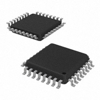
32-Lead LQFP Packaging
32-Lead Pb-Free Package Available
FA SUFFIX
32-LEAD LQFP PACKAGE
CASE 873A-04
Functional Description
The MPC9993 Intelligent Dynamic Clock Switch (IDCS) circuit continuously
monitors both input CLK signals. Upon detection of a failure (CLK stuck HIGH or
LOW for at least 1 period), the INP_BAD for that CLK will be latched (H). If that
CLK is the primary clock, the IDCS will switch to the good secondary clock and
phase/frequency alignment will occur with minimal output phase disturbance.
The typical phase bump caused by a failed clock is eliminated. (See Application
Information section).
AC SUFFIX
32-LEAD LQFP PACKAGE
Pb-FREE PACKAGE
CASE 873A-04
PLL_En
Clk_Selected
Inp1bad
Inp0bad
Man_Override
Dynamic
Switch
Logic
Alarm_Reset
Sel_Clk
Qb0
Qb0
OR
Qb1
Qb1
CLK0
CLK0
CLK1
CLK1
Ext_FB
Ext_FB
÷8
PLL
800 – 1600 MHz
MR
Figure 1. Block Diagram
© Freescale Semiconductor, Inc., 2005. All rights reserved.
÷16
Qb2
Qb2
Qa0
Qa0
Qa1
Qa1
�VCC
Qb0
Qb0
Qb1
Qb1
Qb2
Qb2
VCC
24
23
22
21
20
19
18
17
Qa1
25
16
VCC
Qa1
26
15
Inp0bad
Qa0
27
14
Inp1bad
Qa0
28
13
Clk_Selected
VCC
29
12
GND
VCC_PLL
30
11
Ext_FB
Man_Override
31
10
Ext_FB
PLL_EN
32
MPC9993
3
4
5
6
7
Alarm_Reset
CLK0
CLK0
Sel_Clk
CLK1
CLK1
GND
8
GND
2
MR
9
1
Figure 2. 32-Lead Pinout (Top View)
Table 1. Pin Descriptions
Pin Name
CLK0, CLK0
CLK1, CLK1
Ext_FB, Ext_FB
I/O
Pin Definition
LVPECL Input
LVPECL Input
Differential PLL clock reference (CLK0 pulldown, CLK0 pullup)
Differential PLL clock reference (CLK1 pulldown, CLK1 pullup)
LVPECL Input
Differential PLL feedback clock (Ext_FB pulldown, Ext_FB pullup)
Qa0:1, Qa0:1
LVPECL Output
Differential 1x output pairs
Qb0:2, Qb0:2
LVPECL Output
Differential 2x output pairs
Inp0bad
LVCMOS Output
Indicates detection of a bad input reference clock 0 with respect to the feedback signal. The output is
active HIGH and will remain HIGH until the alarm reset is asserted
Inp1bad
LVCMOS Output
Indicates detection of a bad input reference clock 1 with respect to the feedback signal. The output is
active HIGH and will remain HIGH until the alarm reset is asserted
Clk_Selected
LVCMOS Output
‘0' if clock 0 is selected, ‘1' if clock 1 is selected
Alarm_Reset
LVCMOS Input
‘0' will reset the input bad flags and align Clk_Selected with Sel_Clk. The input is “one-shotted”
(50 kΩ pullup)
Sel_Clk
LVCMOS Input
‘0' selects CLK0, ‘1' selects CLK1 (50 kΩ pulldown)
Manual_Override
LVCMOS Input
‘1' disables internal clock switch circuitry (50 kΩ pulldown)
PLL_En
LVCMOS Input
‘0' bypasses selected input reference around the phase-locked loop (50 kΩ pullup)
MR
LVCMOS Input
‘0' resets the internal dividers forcing Q outputs LOW. Asynchronous to the clock (50 kΩ pullup)
VCCA
Power Supply
PLL power supply
VCC
Power Supply
Digital power supply
GNDA
Power Supply
PLL ground
GND
Power Supply
Digital ground
MPC9993
2
Advanced Clock Drivers Device Data
Freescale Semiconductor
�Table 2. Absolute Maximum Ratings(1)
Symbol
Characteristics
Min
Max
Unit
VCC
Supply Voltage
–0.3
3.9
V
VIN
DC Input Voltage
–0.3
VCC+0.3
V
DC Output Voltage
–0.3
VCC+0.3
V
±20
mA
±50
mA
125
°C
VOUT
IIN
IOUT
TS
DC Input Current
DC Output Current
Storage Temperature
–65
Condition
1. Absolute maximum continuous ratings are those maximum values beyond which damage to the device may occur. Exposure to these
conditions or conditions beyond those indicated may adversely affect device reliability. Functional operation at absolute-maximum-rated
conditions is not implied.
Table 3. General Specifications
Symbol
Characteristics
Min
Typ
Max
VTT
Output termination voltage
MM
ESD Protection (Machine model)
175
V
HBM
ESD Protection (Human body model)
1500
V
CDM
ESD Protection (Charged device model
1000
V
100
LU
Latch-up Immunity
CIN
Input Capacitance
θJA
Thermal Resistance Junction to Ambient
JESD 51-3, single layer test board
JESD 51-6, 2S2P multilayer test board
θJC
Thermal Resistance Junction to Case
TJ
Operating Junction Temperature(1)
(continuous operation)
MTBF = 9.1 years
VCC – 2
Unit
Condition
V
mA
4.0
pF
Inputs
83.1
73.3
68.9
63.8
57.4
86.0
75.4
70.9
65.3
59.6
°C/W
°C/W
°C/W
°C/W
°C/W
Natural convection
100 ft/min
200 ft/min
400 ft/min
800 ft/min
59.0
54.4
52.5
50.4
47.8
60.6
55.7
53.8
51.5
48.8
°C/W
°C/W
°C/W
°C/W
°C/W
Natural convection
100 ft/min
200 ft/min
400 ft/min
800 ft/min
23.0
26.3
°C/W
MIL-SPEC 883E
Method 1012.1
110
°C
1. Operating junction temperature impacts device life time. Maximum continuous operating junction temperature should be selected according
to the application life time requirements (See application note AN1545 for more information). The device AC and DC parameters are
specified up to 110°C junction temperature allowing the MPC9993 to be used in applications requiring industrial temperature range. It is
recommended that users of the MPC9993 employ thermal modeling analysis to assist in applying the junction temperature specifications to
their particular application.
MPC9993
Advanced Clock Drivers Device Data
Freescale Semiconductor
3
�Table 4. DC Characteristics (VCC = 3.3 V ± 5%, TA = – 40° to +85°C)
Symbol
Characteristics
Min
Typ
Max
Unit
Condition
VCC + 0.3
V
0.8
V
±100
µA
VIN = VCC or GND
V
IOH = –24 mA
0.55
V
IOL = 24 mA
0.1
1.3
V
Differential operation
VCC –1.8
VCC –0.3
V
Differential operation
±100
µA
VIN = VCC or GND
LVCMOS control inputs (MR, PLL_En, Sel_Clk, Man_Override, Alarm_Reset)
VIH
Input High Voltage
VIL
Input Low Voltage
IIN
Input
2.0
Current(1)
LVCMOS control outputs (Clk_selected, Inp0bad, Inp1bad)
VOH
Output High Voltage
VOL
Output Low Voltage
LVPECL clock inputs (CLK0, CLK1,
VPP
VCMR
IIN
2.0
Ext_FB)(2)
DC Differential Input Voltage(3)
Differential Cross Point Voltage(4)
Input
Current(1)
LVPECL clock outputs (QA[1:0], QB[2:0])
VOH
Output High Voltage
VCC –1.20
VCC –0.95
VCC –0.70
V
Termination 50 Ω to VTT
VOL
Output Low Voltage
VCC –1.90
VCC –1.75
VCC –1.45
V
Termination 50 Ω to VTT
Maximum Power Supply Current
180
mA
GND Pins
Maximum PLL Supply Current
15
mA
VCC_PLL Pin
Supply Current
IGND
ICC_PLL
1.
2.
3.
4.
Inputs have internal pull-up/pull-down resistors affecting the input current.
Clock inputs driven by differential LVPECL compatible signals.
VPP is the minimum differential input voltage swing required to maintain AC characteristics.
VCMR (DC) is the crosspoint of the differential input signal. Functional operation is obtained when the crosspoint is within the VCMR (DC)
range and the input swing lies within the VPP (DC) specification.
MPC9993
4
Advanced Clock Drivers Device Data
Freescale Semiconductor
�Table 5. AC Characteristics (VCC = 3.3 V ± 5%, TA = –40°C to +85°C)(1)
Symbol
Characteristics
Min
Typ
Max
Unit
fref
Input Reference Frequency
÷16 feedback
50
100
MHz
fVCO
VCO Frequency Range(2)
÷16 feedback
800
1600
MHz
fMAX
Output Frequency
QA[1:0]
QB[2:0]
50
100
100
200
MHz
MHz
frefDC
Reference Input Duty Cycle
t(∅)
Propagation Delay
VPP
Differential Input Voltage(4)
25
75
%
(3)
SPO, static phase offset
CLK0, CLK1 to any Q
-2.0
0.9
+2.0
1.8
ns
ns
(peak-to-peak)
0.25
1.3
V
VCC-1.7
VCC-0.3
V
50
80
ps
ps
20
10
200
100
50
25
400
200
ps
ps
ps
ps
50
55
%
47
ps
10
ms
0.70
ns
(5)
VCMR
Differential Input Crosspoint Voltage
tsk(O)
Output-to-Output Skew
∆per/cycle
Rate of Change of Period
DC
Output Duty Cycle
tJIT(CC)
Cycle-to-Cycle Jitter
tLOCK
Maximum PLL Lock Time
tr, tf
Output Rise/Fall Time
within QA[2:0] or QB[1:0]
within device
QA[1:0](6)
QB[2:0](6)
QA[1:0](7)
QB[2:0](7)
45
RMS (1 σ)
0.05
Condition
PLL locked
PLL locked
PLL_EN=1
PLL_EN=0
20% to 80%
AC characteristics apply for parallel output termination of 50 Ω to VCC – 2 V.
The input reference frequency must match the VCO lock range divided by the feedback divider ratio (FB): fref = fVCO ÷ FB.
CLK0, CLK1 to Ext_FB.
VPP is the minimum differential input voltage swing required to maintain AC characteristics including SPO and device-to-device skew.
Applicable to CLK0, CLK1 and Ext_FB.
5. VCMR (AC) is the crosspoint of the differential input signal. Normal AC operation is obtained when the crosspoint is within the VCMR (AC)
range and the input swing lies within the V PP (AC) specification. Violation of VCMR (AC) or VPP (AC) impacts the SPO, device and part-to-part
skew. Applicable to CLK0, CLK1 and Ext_FB.
6. Specification holds for a clock switch between two input signals (CLK0, CLK1) no greater than 400 ps out of phase. Delta period change per
cycle is averaged over the clock switch excursion.
7. Specification holds for a clock switch between two input signals (CLK0, CLK1) at any phase difference (±180°). Delta period change per
cycle is averaged over the clock switch excursion.
1.
2.
3.
4.
MPC9993
Advanced Clock Drivers Device Data
Freescale Semiconductor
5
�APPLICATIONS INFORMATION
The MPC9993 is a dual clock PLL with on-chip Intelligent
Dynamic Clock Switch (IDCS) circuitry.
Definitions
primary clock: The input CLK selected by Sel_Clk.
secondary clock: The input CLK NOT selected by
Sel_Clk.
PLL reference signal: The CLK selected as the PLL
reference signal by Sel_Clk or IDCS. (IDCS can override
Sel_Clk).
Status Functions
Clk_Selected: Clk_Selected (L) indicates CLK0 is
selected as the PLL reference signal. Clk_Selected (H)
indicates CLK1 is selected as the PLL reference signal.
INP_BAD: Latched (H) when it's CLK is stuck (H) or (L) for
at least one Ext_FB period (Pos to Pos or Neg to Neg).
Cleared (L) on assertion of Alarm_Reset.
Control Functions
Sel_Clk: Sel_Clk (L) selects CLK0 as the primary clock.
Sel_Clk (H) selects CLK1 as the primary clock.
Alarm_Reset: Asserted by a negative edge. Generates a
one-shot reset pulse that clears INPUT_BAD latches and
Clk_Selected latch.
PLL_En: While (L), the PLL reference signal is substituted
for the VCO output.
MR: While (L), internal dividers are held in reset which
holds all Q outputs LOW.
Man Override (H)
(IDCS is disabled, PLL functions normally). PLL reference
signal (as indicated by Clk_Selected) will always be the CLK
selected by Sel_Clk. The status function INP_BAD is active
in Man Override (H) and (L).
Man Override (L)
(IDCS is enabled, PLL functions enhanced). The first CLK
to fail will latch it's INP_BAD (H) status flag and select the
other input as the Clk_Selected for the PLL reference clock.
Once latched, the Clk_Selected and INP_BAD remain
latched until assertion of Alarm_Reset which clears all
latches (INP_BADs are cleared and Clk_Selected = Sel_Clk).
NOTE: If both CLKs are bad when Alarm_Reset is asserted,
both INP_BADs will be latched (H) after one Ext_FB period
and Clk_Selected will be latched (L) indicating CLK0 is the
PLL reference signal. While neither INP_BAD is latched (H),
the Clk_Selected can be freely changed with Sel_Clk.
Whenever a CLK switch occurs, (manually or by IDCS),
following the next negative edge of the newly selected PLL
reference signal, the next positive edge pair of Ext_FB and
the newly selected PLL reference signal will slew to
alignment.
To calculate the overall uncertainty between the input
CLKs and the outputs from multiple MPC9993's, the following
procedure should be used. Assuming that the input CLKs to
all MPC9993's are exactly in phase, the total uncertainty will
be the sum of the static phase offset, max I/O jitter, and output
to output skew.
During a dynamic switch, the output phase between two
devices may be increased for a short period of time. If the two
input CLKs are 400 ps out of phase, a dynamic switch of an
MPC9993 will result in an instantaneous phase change of
400 ps to the PLL reference signal without a corresponding
change in the output phase (due to the limited response of
the PLL). As a result, the I/O phase of a device, undergoing
this switch, will initially be 400 ps and diminish as the PLL
slews to its new phase alignment. This transient timing issue
should be considered when analyzing the overall skew
budget of a system.
Hot insertion and withdrawal
In PECL applications, a powered up driver will experience
a low impedance path through an MPC9993 input to its
powered down VCC pins. In this case, a 100 ohm series
resistance should be used in front of the input pins to limit the
driver current. The resistor will have minimal impact on the
rise and fall times of the input signals.
Acquiring Frequency Lock
1. While the MPC9993 is receiving a valid CLK signal,
assert Man_Override HIGH.
2. The PLL will phase and frequency lock within the
specified lock time.
3. Apply a HIGH to LOW transition to Alarm_Reset to reset
Input Bad flags.
4. De-assert Man_Override LOW to enable Intelligent
Dynamic Clock Switch mode.
MPC9993
6
Advanced Clock Drivers Device Data
Freescale Semiconductor
�PACKAGE DIMENSIONS
PAGE 1 OF 3
CASE 873A-04
ISSUE C
32-LEAD LQFP PACKAGE
MPC9993
Advanced Clock Drivers Device Data
Freescale Semiconductor
7
�PACKAGE DIMENSIONS
PAGE 2 OF 3
CASE 873A-04
ISSUE C
32-LEAD LQFP PACKAGE
MPC9993
8
Advanced Clock Drivers Device Data
Freescale Semiconductor
�PACKAGE DIMENSIONS
PAGE 3 OF 3
CASE 873A-04
ISSUE C
32-LEAD LQFP PACKAGE
MPC9993
Advanced Clock Drivers Device Data
Freescale Semiconductor
9
�NOTES
MPC9993
10
Advanced Clock Drivers Device Data
Freescale Semiconductor
�NOTES
MPC9993
Advanced Clock Drivers Device Data
Freescale Semiconductor
11
�How to Reach Us:
Home Page:
www.freescale.com
E-mail:
support@freescale.com
USA/Europe or Locations Not Listed:
Freescale Semiconductor
Technical Information Center, CH370
1300 N. Alma School Road
Chandler, Arizona 85224
+1-800-521-6274 or +1-480-768-2130
support@freescale.com
Europe, Middle East, and Africa:
Freescale Halbleiter Deutschland GmbH
Technical Information Center
Schatzbogen 7
81829 Muenchen, Germany
+44 1296 380 456 (English)
+46 8 52200080 (English)
+49 89 92103 559 (German)
+33 1 69 35 48 48 (French)
support@freescale.com
Japan:
Freescale Semiconductor Japan Ltd.
Headquarters
ARCO Tower 15F
1-8-1, Shimo-Meguro, Meguro-ku,
Tokyo 153-0064
Japan
0120 191014 or +81 3 5437 9125
support.japan@freescale.com
Asia/Pacific:
Freescale Semiconductor Hong Kong Ltd.
Technical Information Center
2 Dai King Street
Tai Po Industrial Estate
Tai Po, N.T., Hong Kong
+800 2666 8080
support.asia@freescale.com
For Literature Requests Only:
Freescale Semiconductor Literature Distribution Center
P.O. Box 5405
Denver, Colorado 80217
1-800-441-2447 or 303-675-2140
Fax: 303-675-2150
LDCForFreescaleSemiconductor@hibbertgroup.com
MPC9993
Rev. 3
06/2005
Information in this document is provided solely to enable system and software
implementers to use Freescale Semiconductor products. There are no express or
implied copyright licenses granted hereunder to design or fabricate any integrated
circuits or integrated circuits based on the information in this document.
Freescale Semiconductor reserves the right to make changes without further notice to
any products herein. Freescale Semiconductor makes no warranty, representation or
guarantee regarding the suitability of its products for any particular purpose, nor does
Freescale Semiconductor assume any liability arising out of the application or use of any
product or circuit, and specifically disclaims any and all liability, including without
limitation consequential or incidental damages. “Typical” parameters that may be
provided in Freescale Semiconductor data sheets and/or specifications can and do vary
in different applications and actual performance may vary over time. All operating
parameters, including “Typicals”, must be validated for each customer application by
customer’s technical experts. Freescale Semiconductor does not convey any license
under its patent rights nor the rights of others. Freescale Semiconductor products are
not designed, intended, or authorized for use as components in systems intended for
surgical implant into the body, or other applications intended to support or sustain life,
or for any other application in which the failure of the Freescale Semiconductor product
could create a situation where personal injury or death may occur. Should Buyer
purchase or use Freescale Semiconductor products for any such unintended or
unauthorized application, Buyer shall indemnify and hold Freescale Semiconductor and
its officers, employees, subsidiaries, affiliates, and distributors harmless against all
claims, costs, damages, and expenses, and reasonable attorney fees arising out of,
directly or indirectly, any claim of personal injury or death associated with such
unintended or unauthorized use, even if such claim alleges that Freescale
Semiconductor was negligent regarding the design or manufacture of the part.
Freescale™ and the Freescale logo are trademarks of Freescale Semiconductor, Inc.
All other product or service names are the property of their respective owners.
© Freescale Semiconductor, Inc. 2005. All rights reserved.
�