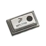
MPL115A1S
Miniature SPI digital barometer, 50 kPa to 115 kPa
Rev. 1.3 — 17 May 2024
Product data sheet
1 General description
The MPL115A1S is an absolute pressure sensor with a digital SPI output targeting low-cost applications. A
miniature 5 x 3 x 1.2 mm LGA package is ideally suited for the space constrained requirements of portable
electronic devices. Low current consumptions of 5 μA during Active mode and 1 μA during Shutdown (Sleep)
mode are essential when focusing on low-power applications. The wide operating temperature range spans
from –40 °C to +105 °C to fit demanding environment conditions.
The MPL115A1S employs a MEMS pressure sensor with a conditioning IC to provide accurate pressure
measurements from 50 kPa to 115 kPa. An integrated ADC converts pressure and temperature sensor readings
to digitized outputs via a SPI port. Factory calibration data is stored internally in an onboard ROM. Utilizing the
raw sensor output and calibration data, the host microcontroller executes a compensation algorithm to render
Compensated Absolute Pressure with ±1 kPa accuracy.
The MPL115A1S pressure sensor’s small form factor, low-power capability, precision, and digital output
optimize it for barometric measurement applications.
2 Features
• Digitized pressure and temperature information together with programmed calibration coefficients for host
micro use.
• Factory calibrated
• 50 kPa to 115 kPa absolute pressure
• ±1 kPa accuracy
• 2.375 V to 5.5 V supply
• Integrated ADC
• SPI Interface
• Monotonic pressure and temperature data outputs
• Surface mount RoHS compliant package
3 Applications
•
•
•
•
•
•
•
Barometry (portable and desktop)
Altimeters
Weather stations
Hard-disk drives (HDD)
Industrial equipment
Health monitoring
Air control systems
�MPL115A1S
NXP Semiconductors
Miniature SPI digital barometer, 50 kPa to 115 kPa
4 Ordering information
Table 1. Ordering information
Type number
MPL115A1S
Package
Name
Description
Version
TSON8
LGA 8 I/O, 3 X 5 X 1.25 PITCH, SENSOR 1.2MAX MM PKG
SOT1769-1
4.1 Ordering options
Table 2. Ordering options
Device Name
Package Options
# of Ports
None
MPL115A1ST1
Tape and Reel (1000)
Single
Pressure Type
Dual
Gauge
Differential
Absolute
•
Digital
Interface
•
SPI
5 Block diagram
VDD
1 µF
ADDR
Coefficient
Storage
ADDR
ADDR
MUX
Diff
Amp
Temp
Sensor
ADC
ADDR
CAP
Pressure
ADDR Temperature
1 µF
SHDN
SCLK
SPI
Interface
DIN
µC
Microcontroller
DOUT
CS
GND
aaa-044101
Figure 1. Block diagram of MPL115A1S
MPL115A1S
Product data sheet
All information provided in this document is subject to legal disclaimers.
Rev. 1.3 — 17 May 2024
© 2024 NXP B.V. All rights reserved.
2 / 23
�MPL115A1S
NXP Semiconductors
Miniature SPI digital barometer, 50 kPa to 115 kPa
6 Pinning information
6.1 Pinning
MPL115A1S
VDD
1
8
SCLK
CAP
2
7
DIN
GND
3
6
DOUT
SHDN
4
5
CS
transparent top view
aaa-044124
Figure 2. Pin configuration
6.2 Pin description
Table 3. Pin description
Pin
Name
Function
1
VDD
Power Supply Connection. VDD range is 2.375 V to 5.5 V.
2
CAP
External Capacitor: Output decoupling capacitor for main internal regulator. Connect a 1 μF
ceramic capacitor to ground.
3
GND
Ground
4
SHDN
5
CS
6
DOUT
7
DIN
8
SCLK
Shutdown: Connect to GND to disable the device. When in shutdown, the part draws no
more than 1 μA supply current and all communications pins (CS, SCLK, DOUT, DIN) are high
impedance. Connect to VDD for normal operation.
Chip Select line.
Serial data output
Serial data input
Serial clock input.
7 Handling and board mount Recommendations
The sensor die is sensitive to light exposure. Direct light exposure through the port hole can lead to varied
accuracy of pressure measurement. Avoid such exposure to the port during normal operation.
7.1 Methods of handling
Components can be picked from the carrier tape using either the vacuum assist or the mechanical type
pickup heads. A vacuum assist nozzle type is most common due to its lower cost of maintenance and ease of
operation. The recommended vacuum nozzle configuration should be designed to make contact with the device
directly on the metal cover and avoid vacuum port location directly over the vent hole in the metal cover of the
device. Multiple vacuum ports within the nozzle may be required to effectively handle the device and prevent
shifting during movement to placement position.
Vacuum pressure required to adequately support the component should be approximately 25 inches Hg
(85 kPa). This level is typical of in-house vacuum supply. Pickup nozzles are available in various sizes and
MPL115A1S
Product data sheet
All information provided in this document is subject to legal disclaimers.
Rev. 1.3 — 17 May 2024
© 2024 NXP B.V. All rights reserved.
3 / 23
�MPL115A1S
NXP Semiconductors
Miniature SPI digital barometer, 50 kPa to 115 kPa
configurations to suit a variety of component geometries. To select the nozzle best suited for the specific
application, NXP recommends that the customer consult their pick and place equipment supplier to determine
the correct nozzle. In some cases, it may be necessary to fabricate a special nozzle depending on the
equipment and speed of operation.
Tweezers or other mechanical forms of handling that have a sharp point are not recommended since they can
inadvertently be inserted into the vent hole of the device. These handling methods can lead to a puncture of the
MEMS element that renders the device inoperable.
7.2 Board mount recommendations
Components can be mounted using solder paste stencil, screen printed or dispensed onto the PCB pads prior
to placement of the component. The volume of solder paste applied to the PCB is normally sufficient to secure
the component during transport to the subsequent reflow soldering process. Use of adhesives to secure the
component is not recommended, but where necessary can be applied to the underside of the device.
Solder pastes are available in variety of metal compositions, particle size, and flux types. The solder paste
consists of metals and flux required for a reliable connection between the component lead and the PCB pad.
Flux aids the removal of oxides that may be present on PCB pads and prevents further oxidation from occurring
during the solder process.
The use of a No-Clean (NC) flux is recommended for exposed cavity components. Using pressure spray, wire
brush, or other methods of cleaning is not recommended since it can puncture the MEMS device and render
it unusable. If cleaning of the PCB is performed, Water Soluble (WS) flux can be used. NXP recommends
protecting the component cavity using adhesive Kapton tape, vinyl cap, or other means prior to the cleaning
process. This covering prevents damage to the MEMS device, contamination, and foreign materials from being
introduced into device cavity as result of cleaning processes.
Ultrasonic cleaning is not recommended as the frequencies can damage wire bond interconnections and the
MEMS device.
MPL115A1S
Product data sheet
All information provided in this document is subject to legal disclaimers.
Rev. 1.3 — 17 May 2024
© 2024 NXP B.V. All rights reserved.
4 / 23
�MPL115A1S
NXP Semiconductors
Miniature SPI digital barometer, 50 kPa to 115 kPa
8 Functional description
Initial
powerup
Reading
coefficient data
Data
conversion
Compensated
pressure reading
Shutdown
aaa-044102
Figure 3. Sequence flowchart
The MPL115A interfaces to a host (or system) microcontroller in the user’s application. All communications are
via SPI. A typical usage sequence is as follows:
Initial power-up
All circuit elements are active. SPI port pins are high impedance and associated registers are cleared. The
device then enters Standby mode.
Reading coefficient data
The user then typically accesses the part and reads the coefficient data. The main circuits within the client
device are disabled during read activity. The coefficients are usually stored in the host microcontroller local
memory but can be re-read at any time.
Reading of the coefficients may be executed only once and the values stored in the host microcontroller. It is not
necessary to read this multiple times because the coefficients within a device are constant and do not change.
However, note that the coefficients are different from device to device, and cannot be used for another part.
Data conversion
This is the first step that is performed each time a new pressure reading is required which is initiated by the
host sending the CONVERT command. The main system circuits are activated (wake) in response to the
command and after the conversion completes, the result is placed into the Pressure and Temperature ADC
output registers.
The conversion completes within the maximum conversion time, tc (see row 6, in Table 11). The device then
enters Standby mode.
MPL115A1S
Product data sheet
All information provided in this document is subject to legal disclaimers.
Rev. 1.3 — 17 May 2024
© 2024 NXP B.V. All rights reserved.
5 / 23
�MPL115A1S
NXP Semiconductors
Miniature SPI digital barometer, 50 kPa to 115 kPa
Compensated pressure reading
After the conversion has been given sufficient time to complete, the host microcontroller reads the result from
the ADC output registers and calculates the Compensated Pressure, a barometric/atmospheric pressure
value which is compensated for changes in temperature and pressure sensor linearity. This is done using the
coefficient data from the MPL115A and the raw sampled pressure and temperature ADC output values, in a
compensation equation (detailed later). Note that this is an absolute pressure measurement with a vacuum as a
reference.
From this step, the host controller may either wait and then return to the Data Conversion step to obtain the next
pressure reading or it may go to the Shutdown step.
Shutdown
For longer periods of inactivity, the user may assert the SHDN input by driving this pin low to reduce system
power consumption. This removes power from all internal circuits, including any registers. In the shutdown
state, the Pressure and Temperature registers are reset, losing any previous ADC output values.
This step is exited by taking the SHDN pin high. Wait for the maximum wake-up time, tw (see row 7, in
Table 11), after which another pressure reading can be taken by transitioning to the data Conversion step.
Table 4. Device memory map
Address
Name
Description
00h
Padc_MSB
10-bit Pressure ADC output value MSB
01h
Padc_LSB
10-bit Pressure ADC output value LSB
02h
Tadc_MSB
10-bit Temperature ADC output value MSB
03h
Tacd_LSB
10-bit Temperature ADC output value LSB
04h
a0_MSB
a0 coefficient MSB
05h
a0_LSB
a0 coefficient LSB
06h
b1_MSB
b1 coefficient MSB
07h
b1_LSB
b1 coefficient LSB
08h
b2_MSB
b2 coefficient MSB
09h
b2_LSB
b2 coefficient LSB
0Ah
c12_MSB
c12 coefficient MSB
0Bh
c12_LSB
c12 coefficient LSB
0Ch
0Dh
0Eh
[1]
—
[1]
—
[1]
—
[1]
reserved
reserved
reserved
0Fh
reserved
—
10h
reserved
—
11h
reserved
—
12h
CONVERT
Start Pressure and Temperature Conversion
[1]
This register is set to 00h. It is reserved, and was previously utilized as Coefficient values, c11 and c22, which were always 00h.
For values with less than 16 bits, the lower LSBs are zero. For example, c12 is 14 bits and is stored into 2 bytes
as follows:
MPL115A1S
Product data sheet
All information provided in this document is subject to legal disclaimers.
Rev. 1.3 — 17 May 2024
© 2024 NXP B.V. All rights reserved.
6 / 23
�MPL115A1S
NXP Semiconductors
Miniature SPI digital barometer, 50 kPa to 115 kPa
c12 MSB = c12[13:6] = [c12b13 , c12b12 , c12b11 , c12b10 , c12b9 , c12b8 , c12b7 , c12b6]
c12 LSB = c12[5:0] & "00" = [c12b5 , c12b4 , c12b3 , c12b2 , c12b1 , c12b0 , 0 , 0]
8.1 Pressure, temperature, and coefficient bit-width specifications
The table below specifies the initial coefficient bit-width specifications for the compensation algorithm and the
specifications for Pressure and Temperature ADC values.
Table 5. Pressure, temperature, and compensation coefficient specifications
a0
b1
b2
c12
Padc
Tadc
Total Bits
16
16
16
14
10
10
Sign Bits
1
1
1
1
0
0
Integer Bits
12
2
1
0
10
10
Fractional Bits
3
13
14
13
0
0
dec pt zero pad
0
0
0
9
0
0
Example Binary Format Definitions:
a0 Signed, Integer Bits = 12, Fractional Bits = 3 :
Coeff a0 = S I11 I10 I9 I8 I7 I6 I5 I4 I3 I2 I1 I0 . F2 F1 F0
b1 Signed, Integer Bits = 2, Fractional Bits = 13 :
Coeff b1 = S I1 I0 . F12 F11 F10 F9 F8 F7 F6 F5 F4 F3 F2 F1 F0
b2 Signed, Integer Bits = 1, Fractional Bits = 14 :
Coeff b2 = S I0 . F13 F12 F11 F10 F9 F8 F7 F6 F5 F4 F3 F2 F1 F0
c12 Signed, Integer Bits = 0, Fractional Bits = 13, dec pt zero pad = 9 :
Coeff c12 = S 0 . 000 000 000 F12 F11 F10 F9 F8 F7 F6 F5 F4 F3 F2 F1 F0
Padc Unsigned, Integer Bits = 10 :
Padc U = I9 I8 I7 I6 I5 I4 I3 I2 I1 I0
Tadc Unsigned, Integer Bits =10 :
Tadc U = I9 I8 I7 I6 I5 I4 I3 I2 I1 I0
Note: Negative coefficients are coded in two’s complement notation.
8.2 Compensation
The 10-bit compensated pressure output, Pcomp, is calculated as follows:
(1)
Where:
Padc is the 10-bit pressure ADC output of the MPL115A
Tadc is the 10-bit temperature ADC output of the MPL115A
a0 is the pressure offset coefficient
b1 is the pressure sensitivity coefficient
b2 is the temperature coefficient of offset (TCO)
c12 is the temperature coefficient of sensitivity (TCS)
Pcomp produces a value of 0 with an input pressure of 50 kPa and produces a full-scale value of 1023 with an
input pressure of 115 kPa.
(2)
MPL115A1S
Product data sheet
All information provided in this document is subject to legal disclaimers.
Rev. 1.3 — 17 May 2024
© 2024 NXP B.V. All rights reserved.
7 / 23
�MPL115A1S
NXP Semiconductors
Miniature SPI digital barometer, 50 kPa to 115 kPa
8.3 Evaluation sequence, arithmetic circuits
The following is an example of the calculation for Pcomp, the compensated pressure output. Input values are in
bold.
c12x2 = c12 * Tadc
a1 = b1 + c12x2
a1x1 = a1 * Padc
y1 = a0 + a1x1
a2x2 = b2 * Tadc
Pcomp = y1 + a2x2
This can be calculated as a succession of Multiply Accumulates (MACs) operations of the form y = a + b * x:
a
y
+
b
X
x
aaa-044109
The polynomial can be evaluated (Equation 1) as a sequence of 3 MACs:
b1
c12
a1
Tadc
y1
a0
Padc
y
b2
PComp
Tadc
aaa-044110
Refer to NXP application note AN3785 for more detailed notes on implementation.
8.4 SPI device read/write operations
All device read/write operations are memory mapped. Device actions, for example, "Start Conversions" are
controlled by writing to the appropriate memory address location. All memory address locations are 6-bit (see
Table 2).
The 8-bit command word comprises:
MPL115A1S
Product data sheet
All information provided in this document is subject to legal disclaimers.
Rev. 1.3 — 17 May 2024
© 2024 NXP B.V. All rights reserved.
8 / 23
�MPL115A1S
NXP Semiconductors
Miniature SPI digital barometer, 50 kPa to 115 kPa
• the most significant bit which is the Read/Write identifier which is '1' for read operations and '0' for write
operations.
• the 6-bit address (from Table 4);
• the least significant bit which is not used and is don't care (X).
The device write commands are shown in Table 6.
Table 6. SPI write command
Legend: X = don't care
Command
Binary
Start Conversions
[1]
HEX
0010010X
[1]
24h
The command byte must be paired with a 00h as part of the SPI exchange to complete the passing of Start Conversions.
The actions taken by the part in response to each command are as follows:
Table 7. SPI Write command description
Command
Action taken
Wake main circuits. Start clock. Allow supply stabilization time. Select pressure
sensor input. Apply positive sensor excitation and perform A to D conversion. Select
temperature input. Perform A to D conversion. Load the Pressure and Temperature
registers with the result. Shut down main circuits and clock.
Start Conversions
SPI Read operations are performed by sending the required address with a leading Read bit set to ‘1’. SPI
operations require that each byte be addressed individually. All data is transmitted most significant bit first.
Table 8. Example SPI Read Commands
Legend: X = don't care
Command
Binary
HEX
[1]
Read Pressure MSB
1000000X
80h
Read Pressure LSB
1000001X
82h
Read Temperature MSB
1000010X
84h
Read Temperature LSB
1000011X
86h
Read Coefficient data byte 1
1000100X
88h
[1]
The command byte must be paired with a 00h as part of the SPI exchange to complete the passing of stated command.
8.5 SPI timing
Table 9 and Figure 4 describe the timing requirements for the SPI system.
Table 9. SPI timing
Ref
Symbol
Function
Min
Max
Unit
1
Of
Operating Frequency
—
8
MHz
2
tSCLK
SCLK Period
125
—
ns
3
tCLKH
SCLK High time
62.5
—
ns
4
tCLKL
SCLK Low time
62.5
—
ns
5
tSCS
Enable lead time
125
—
ns
MPL115A1S
Product data sheet
All information provided in this document is subject to legal disclaimers.
Rev. 1.3 — 17 May 2024
© 2024 NXP B.V. All rights reserved.
9 / 23
�MPL115A1S
NXP Semiconductors
Miniature SPI digital barometer, 50 kPa to 115 kPa
Table 9. SPI timing...continued
Ref
Symbol
Function
Min
Max
Unit
6
tHCS
Enable lag time
125
—
ns
7
tSET
Data setup time
30
—
ns
8
tHOLD
Data hold time
30
—
ns
9
tDDLY
Data valid (after SCLK low edge)
—
32
ns
10
tWCS
Width CS High
30
—
ns
tWCS
CS
SCS
tSCLK
tCLKH
tCLKL
tHCS
SCLK
DIN
tHOLD
tDDLY
DOUT
aaa-044103
Figure 4. SPI timing diagram
8.6 Example of SPI reading of coefficients
These are MPL115A1S SPI commands to read coefficients, execute Pressure and Temperature conversions,
and to read Pressure and Temperature data. The sequence of the commands for the interaction is given
as an example to operate the MPL115A1S. Utilizing this gathered data, an example of the calculating the
Compensated Pressure reading is given in floating point notation.
SPI Commands (simplified for communication)
Command to Write "Convert Pressure and Temperature" = 24h
Command to Read "Pressure ADC High byte" = 80h
Command to Read "Pressure ADC Low byte" = 82h
Command to Read "Temperature ADC High byte" = 84h
Command to Read "Temperature ADC Low byte" = 86h
Command to Read "Coefficient data byte 1 High byte" = 88h
Read coefficients:
[CS=0], [88h], [00h], [8Ah], [00h], [8Ch], [00h], [8Eh], [00h], [90h], [00h], [92h], [00h], [94h], [00h], [96h], [00h],
[00h], [CS=1]
Start pressure and temperature conversion, read raw pressure:
[CS=0], [24h], [00h], [CS=1], [3 ms Delay]
[CS=0], [80h], [00h], [82h], [00h], [84h], [00h], [86h], [00h], [00h], [CS=1]
Note: Extra [00h] at the end of each sequence to output the last data byte on the client side of the SPI.
MPL115A1S
Product data sheet
All information provided in this document is subject to legal disclaimers.
Rev. 1.3 — 17 May 2024
© 2024 NXP B.V. All rights reserved.
10 / 23
�MPL115A1S
NXP Semiconductors
Miniature SPI digital barometer, 50 kPa to 115 kPa
SPI
88
00
8A
00
8C
00
8E
00
90
00
92
00
94
00
96
00
00
00
41
00
DF
00
B0
00
28
00
BE
00
AD
00
38
00
CC
00
DIN
DOUT
CLK
CSB
aaa-044104
Figure 5. SPI read coefficient datagram
a0 coefficient MSB
=
41h
a0 coefficient LSB
=
DFh
b1 coefficient MSB
=
B0h
b1 coefficient LSB
=
28h
b2 coefficient MSB
=
BEh
b2 coefficient LSB
=
ADh
c12 coefficient MSB
=
38h
c12 coefficient LSB
=
CCh
a0 coefficient
=
41DFh
=
2107.875
b1 coefficient
=
B028h
=
–2.49512
b2 coefficient
=
BEADh
=
–1.02069
c12 coefficient
=
38CCh
=
0.00086665
SPI
24
00
00
00
DIN
DOUT
CLK
CSB
aaa-044105
Figure 6. SPI start conversion datagram
Command to start pressure and temperature conversion, 24h.
MPL115A1S
Product data sheet
All information provided in this document is subject to legal disclaimers.
Rev. 1.3 — 17 May 2024
© 2024 NXP B.V. All rights reserved.
11 / 23
�MPL115A1S
NXP Semiconductors
Miniature SPI digital barometer, 50 kPa to 115 kPa
SPI
80
00
82
00
84
00
86
00
00
00
67
00
C0
00
80
00
40
00
DIN
DOUT
CLK
CSB
aaa-044106
Figure 7. SPI read results datagram
Pressure MSB
= 67h
Pressure LSB
= C0h
Pressure
= 67C0h
= 0110 0111 11 00 0000
= 415 ADC counts
Temperature MSB
= 80h
Temperature LSB
= 40h
Temperature
= 8040h
= 1000 0000 01 00 0000
= 513 ADC counts
8.7 Example of pressure compensated calculation in floating-point notation
a0 coefficient
=
2107.875
b1 coefficient
=
–2.49512
b2 coefficient
=
–1.02069
c12 coefficient =
0.00086665
Pressure
=
415 ADC counts
Temperature
=
513 ADC counts
Pressure compensation
Using the evaluation sequence
The evaluation sequence is located in Section 8.3.
c12x2
= c12 * Tadc
a1
= b1 + c12x2 = –2.49512 + 0.44459
= –2.05052
a1x1
= a1 * Padc
= –2.05052 * 415
= –850.96785
y1
= a0 + a1x1
= 2107.875 + (–850.96785)
= 1256.90715
a2x2
= b2 * Tadc
= –1.02069 * 513
= –523.61444
PComp
= y1 + a2x2
= 1256.90715 + (–523.61444)
= 733.29270
MPL115A1S
Product data sheet
= 0.00086665 * 513
= 0.44459
All information provided in this document is subject to legal disclaimers.
Rev. 1.3 — 17 May 2024
© 2024 NXP B.V. All rights reserved.
12 / 23
�MPL115A1S
NXP Semiconductors
Miniature SPI digital barometer, 50 kPa to 115 kPa
9 Maximum ratings
Table 10. Maximum ratings
Voltage (with respect to GND unless otherwise noted)
Symbol
Value
Units
–0.3 to +5.5
V
–0.3 to VDD + 0.3
V
Operating Temperature Range
–40 to +105
°C
Storage Temperature Range
–40 to +125
°C
1000
kPa
VDD
SHDN, SCLK, CS, DIN, DOUT
Overpressure
10 Mechanical and electrical characteristics
Table 11. Mechanical and electrical characteristics
VDD = 2.375 V to 5.5 V, TA = –40 °C to +105 °C, unless otherwise noted. Typical values are at VDD = 3.3 V, TA = +25 °C.
Ref
Parameters
Symbol
1
Operating Supply Voltage
VDD
2
Supply Current
IDD
Conditions
Min
Typ
Max
Units
2.375
3.3
5.5
V
Shutdown (SHDN = GND)
—
—
1
μA
Standby
—
3.5
10
μA
Average – at one measurement per
second
—
5
—
μA
Pressure Sensor
3
Range
50
—
115
kPa
4
Resolution
—
0.15
—
kPa
5
Accuracy
–20 ºC to 85 ºC
—
—
±1
kPa
6
Conversion Time
(Start Pressure and
Temperature Conversion)
tc
Time between start convert command
and data available in the Pressure and
Temperature registers
—
1.6
3
ms
7
Wake-up Time
tw
Time between leaving Shutdown
mode (SHDN goes high) and
communicating with the device to
issue a command or read data.
—
3
5
ms
SPI Inputs: SCLK, CS, DIN
MPL115A1S
Product data sheet
All information provided in this document is subject to legal disclaimers.
Rev. 1.3 — 17 May 2024
© 2024 NXP B.V. All rights reserved.
13 / 23
�MPL115A1S
NXP Semiconductors
Miniature SPI digital barometer, 50 kPa to 115 kPa
Table 11. Mechanical and electrical characteristics...continued
VDD = 2.375 V to 5.5 V, TA = –40 °C to +105 °C, unless otherwise noted. Typical values are at VDD = 3.3 V, TA = +25 °C.
Ref
Parameters
Symbol
Conditions
[1]
Min
Typ
Max
Units
—
—
8
MHz
8
SCLK Clock Frequency
fSCLK
9
Low-level Input Voltage
VIL
—
—
0.3VDD
V
10
High-level Input Voltage
VIH
0.7VDD
—
—
V
V
SPI Outputs: DOUT
11
12
[1]
Low-level Output Voltage
High-level Output Voltage
VOL1
At 3 mA sink current
0
—
0.4
VOL2
At 6 mA sink current
0
—
0.6
VOH1
At 3 mA source current
VDD
– 0.4
—
—
Nominal maximum SPI clock frequency.
MPL115A1S
Product data sheet
All information provided in this document is subject to legal disclaimers.
Rev. 1.3 — 17 May 2024
© 2024 NXP B.V. All rights reserved.
14 / 23
�MPL115A1S
NXP Semiconductors
Miniature SPI digital barometer, 50 kPa to 115 kPa
11 Package outline
Figure 8. Package outline SOT1769-1 (TSON8)
MPL115A1S
Product data sheet
All information provided in this document is subject to legal disclaimers.
Rev. 1.3 — 17 May 2024
© 2024 NXP B.V. All rights reserved.
15 / 23
�MPL115A1S
NXP Semiconductors
Miniature SPI digital barometer, 50 kPa to 115 kPa
Figure 9. Package outline notes SOT1769-1 (TSON8)
MPL115A1S
Product data sheet
All information provided in this document is subject to legal disclaimers.
Rev. 1.3 — 17 May 2024
© 2024 NXP B.V. All rights reserved.
16 / 23
�MPL115A1S
NXP Semiconductors
Miniature SPI digital barometer, 50 kPa to 115 kPa
12 Packing information
Y
0.3 ± 0.05
P2
2.00 ± 0.10 (l)
E1
1.75 ± 0.10
Po
4.00 ± 0.10 (ll)
Do
Ø 1.55 ± 0.05
Bo
REF. 6°
F (lll)
D1
Ø 1.50 min
W
X
REF. 30°
X
Typ. R 0.25
Ao
P1
Ko
Y
REF. 30°
SECTION Y-Y
SCALE 3.5 : 1
REF. 6°
SECTION X-X
SCALE 3.5 : 1
P1
8.00 ± 0.10
Measured from centerline of sprocket hole to
centerline of pocket.
(lI) Cumulative tolerance of 10 sprocket holes is
± 0.20.
(lIl) Measured from centerline of sprocket hole to
centerline of pocket.
(lV) Other material available.
W
12.00 ± 0.10
Dimensions are in millimeters.
Ao
3.35 ± 0.10
Bo
5.35 ± 0.10
Ko
1.20 ± 0.10
F
5.50 ± 0.10
(I)
aaa-044107
Figure 10. LGA (3 x 5) embossed carrier tape dimensions
Pin 1 Index Area
aaa-044108
Figure 11. Device orientation in chip carrier
MPL115A1S
Product data sheet
All information provided in this document is subject to legal disclaimers.
Rev. 1.3 — 17 May 2024
© 2024 NXP B.V. All rights reserved.
17 / 23
�MPL115A1S
NXP Semiconductors
Miniature SPI digital barometer, 50 kPa to 115 kPa
13 Soldering
1. Use SAC solder alloy, Sn-Ag-Cu, with a melting point of about 217 °C. NXP recommends using SAC305,
Sn-3.0 wt.% Ag-0.5 wt.% Cu.
2. Reflow
• Ramp up rate: 2 °C/s to 3 °C/s.
• Preheat flat (soak): 110 s to 130 s.
• Reflow peak temperature: 250 °C to 260 °C (depends on exact SAC alloy composition).
• Time above 217°C: 40 s to 90 s (depends on board type, thermal mass of the board/quantities in the
reflow).
• Ramp down: 5 °C/s to 6 °C/s.
• Using an inert reflow environment (with O2 level about 5 ppm to 15 ppm).
Note: The stress level and signal offset of the device also depends on the board type, board core material,
board thickness, and metal finishing of the board.
14 Soldering/landing pad information
The LGA package is compliant with the RoHS standard. NXP recommends using a no-clean solder paste to
reduce cleaning exposure to high pressure and chemical agents that can damage or reduce life span of the
Pressure sensing element.
pin 1 index area
8
1
0.55 (8x)
0.625 (2x)
1.25 (6x)
0.10 (8x)
5
0.5 ± 0.05
(8x)
0.8 ± 0.05
(8x)
4
0.05 (8x)
1.0
(8x)
BLACK for Package Outline
RED for PCB Landing Pattern
aaa-046324
Figure 12. Recommended PCB landing pattern
MPL115A1S
Product data sheet
All information provided in this document is subject to legal disclaimers.
Rev. 1.3 — 17 May 2024
© 2024 NXP B.V. All rights reserved.
18 / 23
�MPL115A1S
NXP Semiconductors
Miniature SPI digital barometer, 50 kPa to 115 kPa
15 Revision history
Table 12. Revision history
Document ID
Release date
Description
MPL115A1S v.1.3
17 May 2024
• MPL115A1S v.1.3 supercedes MPL115A1S v.1.2.
• MPL115A1S v.1.3 is a product data sheet.
• Updated the document formatting, revision history and legal
information sections to comply with new NXP documentation
guidelines.
• Section 12, Figure 10, revised dimension "T" from "0.25 ± 0.05"
to "0.3 ± 0.05".
MPL115A1S v.1.2
8 May 2023
• MPL115A1S v.1.2 supercedes MPL115A1S v.1.1.
• MPL115A1S v.1.1 is a product data sheet, updated the data
sheet status from "Objective" to "Product".
MPL115A1S v.1.1
16 May 2022
• MPL115A1S v.1.1 supercedes MPL115A1S v.1.
• MPL115A1S v.1.1 is an objective data sheet.
• Global changes as follows:
– Revised cover page image.
– Performed minor grammatical and typographical corrections
throughout.
– Updated all images to conform to NXP image standards.
– Changed all references of "slave" to "client" to conform to the
NXP inclusive language intiative.
• Section 4, Table 2: Removed the row "MPL115A1S" with "Tray"
in the "Package Options" column.
• Section 11, split the package outline images into separate
figures.
MPL115A1S v.1
7 October 2021
• MPL115A1S v.1 is an objective data sheet.
Initial release.
MPL115A1S
Product data sheet
All information provided in this document is subject to legal disclaimers.
Rev. 1.3 — 17 May 2024
© 2024 NXP B.V. All rights reserved.
19 / 23
�MPL115A1S
NXP Semiconductors
Miniature SPI digital barometer, 50 kPa to 115 kPa
Legal information
Data sheet status
Document status
[1][2]
Product status
[3]
Definition
Objective [short] data sheet
Development
This document contains data from the objective specification for product
development.
Preliminary [short] data sheet
Qualification
This document contains data from the preliminary specification.
Product [short] data sheet
Production
This document contains the product specification.
[1]
[2]
[3]
Please consult the most recently issued document before initiating or completing a design.
The term 'short data sheet' is explained in section "Definitions".
The product status of device(s) described in this document may have changed since this document was published and may differ in case of multiple
devices. The latest product status information is available on the Internet at URL https://www.nxp.com.
Definitions
Draft — A draft status on a document indicates that the content is still
under internal review and subject to formal approval, which may result
in modifications or additions. NXP Semiconductors does not give any
representations or warranties as to the accuracy or completeness of
information included in a draft version of a document and shall have no
liability for the consequences of use of such information.
Short data sheet — A short data sheet is an extract from a full data sheet
with the same product type number(s) and title. A short data sheet is
intended for quick reference only and should not be relied upon to contain
detailed and full information. For detailed and full information see the
relevant full data sheet, which is available on request via the local NXP
Semiconductors sales office. In case of any inconsistency or conflict with the
short data sheet, the full data sheet shall prevail.
Product specification — The information and data provided in a Product
data sheet shall define the specification of the product as agreed between
NXP Semiconductors and its customer, unless NXP Semiconductors and
customer have explicitly agreed otherwise in writing. In no event however,
shall an agreement be valid in which the NXP Semiconductors product
is deemed to offer functions and qualities beyond those described in the
Product data sheet.
Disclaimers
Limited warranty and liability — Information in this document is believed
to be accurate and reliable. However, NXP Semiconductors does not give
any representations or warranties, expressed or implied, as to the accuracy
or completeness of such information and shall have no liability for the
consequences of use of such information. NXP Semiconductors takes no
responsibility for the content in this document if provided by an information
source outside of NXP Semiconductors.
In no event shall NXP Semiconductors be liable for any indirect, incidental,
punitive, special or consequential damages (including - without limitation lost profits, lost savings, business interruption, costs related to the removal
or replacement of any products or rework charges) whether or not such
damages are based on tort (including negligence), warranty, breach of
contract or any other legal theory.
Notwithstanding any damages that customer might incur for any reason
whatsoever, NXP Semiconductors’ aggregate and cumulative liability
towards customer for the products described herein shall be limited in
accordance with the Terms and conditions of commercial sale of NXP
Semiconductors.
Applications — Applications that are described herein for any of these
products are for illustrative purposes only. NXP Semiconductors makes no
representation or warranty that such applications will be suitable for the
specified use without further testing or modification.
Customers are responsible for the design and operation of their
applications and products using NXP Semiconductors products, and NXP
Semiconductors accepts no liability for any assistance with applications or
customer product design. It is customer’s sole responsibility to determine
whether the NXP Semiconductors product is suitable and fit for the
customer’s applications and products planned, as well as for the planned
application and use of customer’s third party customer(s). Customers should
provide appropriate design and operating safeguards to minimize the risks
associated with their applications and products.
NXP Semiconductors does not accept any liability related to any default,
damage, costs or problem which is based on any weakness or default
in the customer’s applications or products, or the application or use by
customer’s third party customer(s). Customer is responsible for doing all
necessary testing for the customer’s applications and products using NXP
Semiconductors products in order to avoid a default of the applications
and the products or of the application or use by customer’s third party
customer(s). NXP does not accept any liability in this respect.
Limiting values — Stress above one or more limiting values (as defined in
the Absolute Maximum Ratings System of IEC 60134) will cause permanent
damage to the device. Limiting values are stress ratings only and (proper)
operation of the device at these or any other conditions above those
given in the Recommended operating conditions section (if present) or the
Characteristics sections of this document is not warranted. Constant or
repeated exposure to limiting values will permanently and irreversibly affect
the quality and reliability of the device.
Terms and conditions of commercial sale — NXP Semiconductors
products are sold subject to the general terms and conditions of commercial
sale, as published at https://www.nxp.com/profile/terms, unless otherwise
agreed in a valid written individual agreement. In case an individual
agreement is concluded only the terms and conditions of the respective
agreement shall apply. NXP Semiconductors hereby expressly objects to
applying the customer’s general terms and conditions with regard to the
purchase of NXP Semiconductors products by customer.
No offer to sell or license — Nothing in this document may be interpreted
or construed as an offer to sell products that is open for acceptance or
the grant, conveyance or implication of any license under any copyrights,
patents or other industrial or intellectual property rights.
Export control — This document as well as the item(s) described herein
may be subject to export control regulations. Export might require a prior
authorization from competent authorities.
Right to make changes — NXP Semiconductors reserves the right to
make changes to information published in this document, including without
limitation specifications and product descriptions, at any time and without
notice. This document supersedes and replaces all information supplied prior
to the publication hereof.
MPL115A1S
Product data sheet
All information provided in this document is subject to legal disclaimers.
Rev. 1.3 — 17 May 2024
© 2024 NXP B.V. All rights reserved.
20 / 23
�MPL115A1S
NXP Semiconductors
Miniature SPI digital barometer, 50 kPa to 115 kPa
Suitability for use in non-automotive qualified products — Unless
this document expressly states that this specific NXP Semiconductors
product is automotive qualified, the product is not suitable for automotive
use. It is neither qualified nor tested in accordance with automotive testing
or application requirements. NXP Semiconductors accepts no liability for
inclusion and/or use of non-automotive qualified products in automotive
equipment or applications.
In the event that customer uses the product for design-in and use in
automotive applications to automotive specifications and standards,
customer (a) shall use the product without NXP Semiconductors’ warranty
of the product for such automotive applications, use and specifications, and
(b) whenever customer uses the product for automotive applications beyond
NXP Semiconductors’ specifications such use shall be solely at customer’s
own risk, and (c) customer fully indemnifies NXP Semiconductors for any
liability, damages or failed product claims resulting from customer design and
use of the product for automotive applications beyond NXP Semiconductors’
standard warranty and NXP Semiconductors’ product specifications.
Suitability for use in industrial applications (functional safety) — This
NXP product has been qualified for use in industrial applications. It has
been developed in accordance with IEC 61508, and has been SIL-classified
accordingly. If this product is used by customer in the development of, or for
incorporation into, products or services (a) used in safety critical applications
or (b) in which failure could lead to death, personal injury, or severe physical
or environmental damage (such products and services hereinafter referred
to as “Critical Applications”), then customer makes the ultimate design
decisions regarding its products and is solely responsible for compliance with
all legal, regulatory, safety, and security related requirements concerning
its products, regardless of any information or support that may be provided
by NXP. As such, customer assumes all risk related to use of any products
in Critical Applications and NXP and its suppliers shall not be liable for
any such use by customer. Accordingly, customer will indemnify and hold
NXP harmless from any claims, liabilities, damages and associated costs
and expenses (including attorneys’ fees) that NXP may incur related to
customer’s incorporation of any product in a Critical Application.
Translations — A non-English (translated) version of a document, including
the legal information in that document, is for reference only. The English
version shall prevail in case of any discrepancy between the translated and
English versions.
NXP B.V. — NXP B.V. is not an operating company and it does not distribute
or sell products.
Security — Customer understands that all NXP products may be subject to
unidentified vulnerabilities or may support established security standards or
specifications with known limitations. Customer is responsible for the design
and operation of its applications and products throughout their lifecycles
to reduce the effect of these vulnerabilities on customer’s applications
and products. Customer’s responsibility also extends to other open and/or
proprietary technologies supported by NXP products for use in customer’s
applications. NXP accepts no liability for any vulnerability. Customer should
regularly check security updates from NXP and follow up appropriately.
Customer shall select products with security features that best meet rules,
regulations, and standards of the intended application and make the
ultimate design decisions regarding its products and is solely responsible
for compliance with all legal, regulatory, and security related requirements
concerning its products, regardless of any information or support that may be
provided by NXP.
NXP has a Product Security Incident Response Team (PSIRT) (reachable
at PSIRT@nxp.com) that manages the investigation, reporting, and solution
release to security vulnerabilities of NXP products.
MPL115A1S
Product data sheet
Trademarks
Notice: All referenced brands, product names, service names, and
trademarks are the property of their respective owners.
NXP — wordmark and logo are trademarks of NXP B.V.
All information provided in this document is subject to legal disclaimers.
Rev. 1.3 — 17 May 2024
© 2024 NXP B.V. All rights reserved.
21 / 23
�MPL115A1S
NXP Semiconductors
Miniature SPI digital barometer, 50 kPa to 115 kPa
Tables
Tab. 1.
Tab. 2.
Tab. 3.
Tab. 4.
Tab. 5.
Tab. 6.
Ordering information ..........................................2
Ordering options ................................................2
Pin description ...................................................3
Device memory map ......................................... 6
Pressure, temperature, and compensation
coefficient specifications ....................................7
SPI write command ...........................................9
Tab. 7.
Tab. 8.
Tab. 9.
Tab. 10.
Tab. 11.
Tab. 12.
SPI Write command description ........................ 9
Example SPI Read Commands ........................ 9
SPI timing ..........................................................9
Maximum ratings ............................................. 13
Mechanical and electrical characteristics ........ 13
Revision history ...............................................19
Fig. 8.
Fig. 9.
Package outline SOT1769-1 (TSON8) ............ 15
Package outline notes SOT1769-1
(TSON8) .......................................................... 16
LGA (3 x 5) embossed carrier tape
dimensions ...................................................... 17
Device orientation in chip carrier .....................17
Recommended PCB landing pattern ............... 18
Figures
Fig. 1.
Fig. 2.
Fig. 3.
Fig. 4.
Fig. 5.
Fig. 6.
Fig. 7.
Block diagram of MPL115A1S .......................... 2
Pin configuration ............................................... 3
Sequence flowchart ...........................................5
SPI timing diagram ..........................................10
SPI read coefficient datagram ......................... 11
SPI start conversion datagram ........................11
SPI read results datagram .............................. 12
MPL115A1S
Product data sheet
Fig. 10.
Fig. 11.
Fig. 12.
All information provided in this document is subject to legal disclaimers.
Rev. 1.3 — 17 May 2024
© 2024 NXP B.V. All rights reserved.
22 / 23
�MPL115A1S
NXP Semiconductors
Miniature SPI digital barometer, 50 kPa to 115 kPa
Contents
1
2
3
4
4.1
5
6
6.1
6.2
7
7.1
7.2
8
8.1
8.2
8.3
8.4
8.5
8.6
8.7
9
10
11
12
13
14
15
General description ......................................... 1
Features ............................................................ 1
Applications ..................................................... 1
Ordering information .......................................2
Ordering options ................................................ 2
Block diagram ..................................................2
Pinning information .........................................3
Pinning ............................................................... 3
Pin description ................................................... 3
Handling and board mount
Recommendations ...........................................3
Methods of handling .......................................... 3
Board mount recommendations .........................4
Functional description .................................... 5
Pressure, temperature, and coefficient bitwidth specifications ............................................7
Compensation ....................................................7
Evaluation sequence, arithmetic circuits ............8
SPI device read/write operations ....................... 8
SPI timing .......................................................... 9
Example of SPI reading of coefficients ............ 10
Example of pressure compensated
calculation in floating-point notation .................12
Maximum ratings ........................................... 13
Mechanical and electrical characteristics ... 13
Package outline ............................................. 15
Packing information ...................................... 17
Soldering ........................................................ 18
Soldering/landing pad information .............. 18
Revision history .............................................19
Legal information ...........................................20
Please be aware that important notices concerning this document and the product(s)
described herein, have been included in section 'Legal information'.
© 2024 NXP B.V.
All rights reserved.
For more information, please visit: https://www.nxp.com
Date of release: 17 May 2024
Document identifier: MPL115A1S
�