MPX5010-MPXV5010-MPVZ5010
Integrated silicon pressure sensor on-chip signal conditioned, temperature
compensated and calibrated
Rev. 14 — 17 May 2024
Product data sheet
1 General description
The MPxx5010 series piezoresistive transducers are state-of-the-art monolithic silicon pressure sensors
designed for a wide range of applications, but particularly those employing a microcontroller or microprocessor
with A/D inputs. This transducer combines advanced micromachining techniques, thin-film metallization, and
bipolar processing to provide an accurate, high level analog output signal that is proportional to the applied
pressure. The axial port has been modified to accommodate industrial grade tubing.
2 Features and benefits
•
•
•
•
•
•
•
5.0% maximum error over 0° to 85° C
Ideally suited for microprocessor or microcontroller-based systems
Durable epoxy unibody and thermoplastic (PPS) surface mount package
Temperature compensated over –40° to +125° C
Patented silicon shear stress strain gauge
Available in differential and gauge configurations
Available in surface mount (SMT) or through-hole (DIP) configurations
3 Applications
•
•
•
•
•
•
•
Hospital beds
HVAC
Respiratory systems
Process control
Washing machine water level measurement (Reference AN1950)
Ideally suited for microprocessor or microcontroller-based systems
Appliance liquid level and pressure measurement
�MPX5010-MPXV5010-MPVZ5010
NXP Semiconductors
Integrated silicon pressure sensor on-chip signal conditioned, temperature compensated and
calibrated
4 Ordering information
Table 1. Ordering information
Type number
Package
Name
Description
Version
Unibody package (MPX5010 series)
MPX5010DP
SENSOR4F sensor package, 6 terminals, 2.54 mm pitch, 17.78 mm x 29.48 mm x
10.67 body
SOT1756-1
MPX5010GP
SENSOR6F sensor package, 6 terminals, 2.54 mm pitch, 17.78 mm x 29.47 mm x
8.01 mm body
SOT1852-1
Small outline package (MPXV5010 series)
MPXV5010DP
S08
plastic, small outline package, 8 terminals, 2.54 mm pitch, 12.06. mm x
12.06 mm x 7.62 mm body
SOT1693-1
MPXV5010GC6T1 S08
plastic, small outline package, 8 terminals, 2.54 mm pitch, 10.67. mm x
10.67 mm x 12.96 mm body
SOT1854-1
MPXV5010GC7U
S08
plastic, small outline package, 8 terminals, 2.54 mm pitch, 10.67. mm x
10.67 mm x 12.96 mm body
SOT1863-1
MPXV5010GP
S08
plastic, small outline package, 8 terminals, 2.54 mm pitch, 12.06. mm x
12.06 mm x 7.62 mm body
SOT1693-3
Small outline package (Media resistant gel) (MPVZ5010 series)
MPVZ5010GW6U
S08
plastic, small outline package, 8 terminals, 2.54 mm pitch, 1.07 mm x 1.07 SOT1691-2
mm x 1.99 mm body
MPVZ5010GW7U
S08
plastic, small outline package, 8 terminals, 2.54 mm pitch, 1.07 mm x 1.07 SOT1691-1
mm x 1.99 mm body
4.1 Ordering options
Table 2. Ordering options
ORDERING INFORMATION
Device Name
Case No.
# of Ports
None
Single
Pressure Type
Dual
Gauge
Differential Absolute
Device
Marking
Unibody Package (MPX5010 Series)
MPX5010DP
867C
MPX5010GP
867B
•
•
•
•
MPX5010DP
MPX5010GP
Small Outline Package (MPXV5010 Series)
MPXV5010DP
1351
•
•
MPXV5010DP
MPXV5010GC6T1
482A
•
•
MPXV5010G
MPXV5010GC7U
482C
•
•
MPXV5010G
MPXV5010GP
1369
•
•
MPXV5010GP
Small Outline Package (Media Resistant Gel) (MPVZ5010 Series)
MPVZ5010GW6U
1735
•
•
MZ5010GW
MPVZ5010GW7U
1560
•
•
MZ5010GW
MPX5010
Product data sheet
All information provided in this document is subject to legal disclaimers.
Rev. 14 — 17 May 2024
© 2024 NXP B.V. All rights reserved.
2 / 32
�MPX5010-MPXV5010-MPVZ5010
NXP Semiconductors
Integrated silicon pressure sensor on-chip signal conditioned, temperature compensated and
calibrated
5 Block diagram
Figure 1 shows a block diagram of the internal circuitry integrated on a pressure sensor chip.
VS
Thin film
temperature
compensation
and
gain stage #1
Sensing
element
GND
Gain stage #2
and ground
reference
shift circuitry
Vout
Pins 4, 5 and 6 are NO CONNECTS
for unibody device
Pins 1, 5, 6, 7 and 8 are NO CONNECTS
for small outline package device
aaa-051151
Figure 1. Fully Integrated Pressure Sensor Schematic
6 Pinning information
6.1 Pinning - Unibody packages
1 2 3 4 5 6
VOUT
GND
VS
n.c.
n.c.
n.c.
aaa-055124
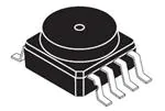
Figure 2. MPX5010DP - SOT1756-1 - Case 867C-05
1 2 3 4 5 6
VOUT
GND
VS
n.c.
n.c.
n.c.
aaa-054997
Figure 3. MPX5010GP - SOT1852-1 - Case 867B-04
MPX5010
Product data sheet
All information provided in this document is subject to legal disclaimers.
Rev. 14 — 17 May 2024
© 2024 NXP B.V. All rights reserved.
3 / 32
�MPX5010-MPXV5010-MPVZ5010
NXP Semiconductors
Integrated silicon pressure sensor on-chip signal conditioned, temperature compensated and
calibrated
6.2 Pin description - Unibody packages
Table 3. Pin descriptions - Unibody pacakages
This table defines the pin configuration for the Unibody packages indentified in Table 1.
Symbol
Pin
Description
VOUT
1
VOUT
GND
2
Ground
VS
3
Supply voltage
N.C.
4
No connect
N.C.
5
No connect
N.C.
6
No connect
6.3 Pinning - Small Outline packages
n.c.
1
8
n.c.
Vs
2
7
n.c.
GND
3
6
n.c.
Vout
4
5
n.c.
aaa-051259
Figure 4. MPXV5010DP - SOT1693-1 - Case 1351-01
n.c.
1
8
n.c.
VS
2
7
n.c.
GND
3
6
n.c.
VOUT
4
5
n.c.
aaa-051261
Figure 5. MPXV5010GC6T1 - SOT1854-1 - Case 482A-01
n.c.
1
8
n.c.
VS
2
7
n.c.
GND
3
6
n.c.
VOUT
4
5
n.c.
aaa-051261
Figure 6. MPXV5010GC7U - SOT1863-1 - Case 482C-03
MPX5010
Product data sheet
All information provided in this document is subject to legal disclaimers.
Rev. 14 — 17 May 2024
© 2024 NXP B.V. All rights reserved.
4 / 32
�MPX5010-MPXV5010-MPVZ5010
NXP Semiconductors
Integrated silicon pressure sensor on-chip signal conditioned, temperature compensated and
calibrated
n.c.
1
8
n.c.
VS
2
7
n.c.
GND
3
6
n.c.
VOUT
4
5
n.c.
aaa-051260
Figure 7. MPXV5010GP - SOT1693-3 - Case 1369-01
n.c.
1
8
n.c.
VS
2
7
n.c.
GND
3
6
n.c.
VOUT
4
5
n.c.
aaa-055550
Figure 8. MPVZ5010GW6U - SOT1691-2 - Case 1735-01
n.c. 1
8 n.c.
VS 2
7 n.c.
GND 3
6 n.c.
VOUT 4
5 n.c.
aaa-055551
Figure 9. MPVZ5010GW7U - SOT1691-1 - Case 1560-02
6.4 Pin description - Small Outline packages
Table 4. Pin descriptions - Small Outline packages
This table defines the pin configuration for the Small Outline packages indentified in Table 1.
Symbol
Pin
Description
N.C.
1
No connect
VS
2
Supply voltage
GND
3
Ground
VOUT
4
VOUT
N.C.
5
No connect
N.C.
6
No connect
N.C.
7
No connect
N.C.
8
No connect
MPX5010
Product data sheet
All information provided in this document is subject to legal disclaimers.
Rev. 14 — 17 May 2024
© 2024 NXP B.V. All rights reserved.
5 / 32
�MPX5010-MPXV5010-MPVZ5010
NXP Semiconductors
Integrated silicon pressure sensor on-chip signal conditioned, temperature compensated and
calibrated
7 Limiting values
Table 5. Limiting values
[1]
Rating
Symbol
Value
Unit
Maximum Pressure (P1 > P2)
Pmax
40
kPa
Storage Temperature
Tstg
–40 to +125
°C
Operating Temperature
TA
–40 to +125
°C
[1]
Exposure beyond the specified limits may cause permanent damage or degradation to the device.
8 Recommended operating conditions
Table 6. Recommended operating conditions
VS = 5.0 Vdc, TA = 25°C unless otherwise noted, P1 > P2. Decoupling circuit shown in Figure 11 required to meet
specification.)
Characteristic
Symbol
Min
Typ
Max
Unit
POP
0
—
10
1019.78
kPa
mm H2O
VS
4.75
5.0
5.25
Vdc
Io
—
5.0
10
mAdc
Voff
0
0.2
0.425
Vdc
VFSO
4.475
4.7
4.925
Vdc
VFSS
4.275
4.5
4.725
Vdc
—
—
—
±5.0
%VFSS
V/P
—
450
4.413
—
mV/kPa
mV/
kPA H2O
Response Time
tR
—
1.0
—
ms
Output Source Current at Full Scale Output
IO+
—
0.1
—
mAdc
—
—
20
—
ms
—
—
± 0.5
—
%VFSS
Pressure Range
[1]
Supply Voltage
Supply Current
Minimum Pressure Offset
@ VS = 5.0 Volts
[2]
(0 to 85°C)
[3]
Full Scale Output (0 to 85°C)
@ VS = 5.0 Volts
[4]
Full Scale Span (0 to 85°C)
@ VS = 5.0 Volts
[5]
Accuracy (0 to 85°C)
Sensitivity
[6]
[7]
Warm-Up Time
Offset Stability
[1]
[2]
[3]
[4]
[5]
[8]
Device is ratiometric within this specified excitation range.
Offset (Voff) is defined as the output voltage at the minimum rated pressure.
Full Scale Output (VFSO) is defined as the output voltage at the maximum or full rated pressure.
Full Scale Span (VFSS) is defined as the algebraic difference between the output voltage at full rated pressure and the output voltage at the minimum rated
pressure.
Accuracy (error budget) consists of the following:
Linearity: Output deviation from a straight line relationship with pressure over the specified pressure range.
Temperature Hysteresis: Output deviation at any temperature within the operating temperature range, after the temperature is cycled to and from the
minimum or maximum operating temperature points, with zero differential pressure applied.
Pressure Hysteresis: Output deviation at any pressure within the specified range, when this pressure is cycled to and from the minimum or
maximum rated pressure, at 25°C.
TcSpan: Output deviation over the temperature range of 0° to 85°C, relative to 25°C.
TcOffset: Output deviation with minimum rated pressure applied, over the temperature range of 0° to 85°C, relative to 25°C.
Variation from Nominal:The variation from nominal values, for Offset or Full Scale Span, as a percent of VFSS, at 25°C.
MPX5010
Product data sheet
All information provided in this document is subject to legal disclaimers.
Rev. 14 — 17 May 2024
© 2024 NXP B.V. All rights reserved.
6 / 32
�MPX5010-MPXV5010-MPVZ5010
NXP Semiconductors
Integrated silicon pressure sensor on-chip signal conditioned, temperature compensated and
calibrated
[6]
[7]
[8]
Response Time is defined as the time for the incremental change in the output to go from 10% to 90% of its final value when subjected to a specified step
change in pressure.
Warm-up Time is defined as the time required for the product to meet the specified output voltage after the Pressure has been stabilized.
Offset Stability is the product's output deviation when subjected to 1000 hours of Pulsed Pressure, Temperature Cycling with Bias Test.
9 On-chip temperature compensation and calibration
The performance over temperature is achieved by integrating the shear-stress strain gauge, temperature
compensation, calibration and signal conditioning circuitry onto a single monolithic chip.
Figure 10 illustrates the differential or gauge configuration in the basic chip carrier (Case 482). A fluorosilicone
gel isolates the die surface and wire bonds from the environment, while allowing the pressure signal to be
transmitted to the sensor diaphragm.
The MPxx5010G series pressure sensor operating characteristics, and internal reliability and qualification tests
are based on use of dry air as the pressure media. Media, other than dry air, may have adverse effects on
sensor performance and long-term reliability. Contact the factory for information regarding media compatibility in
your application.
Figure 11 shows the recommended decoupling circuit for interfacing the integrated sensor to the A/D input of a
microprocessor or microcontroller. Proper decoupling of the power supply is recommended.
Figure 12 shows the sensor output signal relative to pressure input. Typical, minimum, and maximum output
curves are shown for operation over a temperature range of 0° to 85°C using the decoupling circuit shown in
Figure 11. The output will saturate outside of the specified pressure range.
Fluoro silicone
gel die coat
Die
Stainless
steel cap
P1
Thermoplastic
case
Wire bond
Lead frame
P2
Differential sensing element
Die bond
aaa-054999
Figure 10. Cross-sectional diagram SOP (not to scale)
+5 V
OUTPUT
Vout
VS
IPS
1.0 µF
0.01 µF
GND
470 pF
aaa-040608
Figure 11. Recommended power supply decoupling and output filtering
Note: For additional output filtering, please refer to Application Note AN1646.
MPX5010
Product data sheet
All information provided in this document is subject to legal disclaimers.
Rev. 14 — 17 May 2024
© 2024 NXP B.V. All rights reserved.
7 / 32
�MPX5010-MPXV5010-MPVZ5010
NXP Semiconductors
Integrated silicon pressure sensor on-chip signal conditioned, temperature compensated and
calibrated
aaa-055000
5.0
Transfer function (kPa):
Vout = VS × (0.09 × P + 0.04) ± 5.0 VFSS
VS = 5.0 Vdc
TEMP = 0 to 85°C
Output
(V)
4.0
3.0
Max
Typical
2.0
Min
1.0
0
0
2.0
4.0
6.0
8.0
Differential pressure (kPa)
10.0
Figure 12. Output vs. Pressure Differential
Nominal Transfer Value:
4
Temperature
error
factor 3
2
Temp
Multiplier
-40
0 to 85
+125
3
1
3
1
0
-40
-20
0
20
40
60
80
100
120
140
Temperature in °C
aaa-051150
Figure 13. Temperature error band
MPX5010
Product data sheet
All information provided in this document is subject to legal disclaimers.
Rev. 14 — 17 May 2024
© 2024 NXP B.V. All rights reserved.
8 / 32
�MPX5010-MPXV5010-MPVZ5010
NXP Semiconductors
Integrated silicon pressure sensor on-chip signal conditioned, temperature compensated and
calibrated
0.5
0.4
0.3
0.2
0.1
Pressure
error
0.0
(kPa)
-0.1
0
1
2
3
4
5
6
7
8
9
10
Pressure (kPa)
-0.2
-0.3
-0.4
-0.5
Pressure
Error (max)
0 to 10 (kPa)
± 0.5 (kPa)
aaa-055001
Figure 14. Pressure error band
10 Pressure (P1) / Vacuum (P2) side identification table
NXP designates the two sides of the pressure sensor as the Pressure (P1) side and the Vacuum (P2) side. The
Pressure (P1) side is the side containing fluorosilicone gel which protects the die from harsh media. The MPX
pressure sensor is designed to operate with positive differential pressure applied, P1 > P2.
The Pressure (P1) side may be identified by using Table 7.
Table 7. Pressure (P1) side identification
Part Number
Case Type
Pressure (P1) Side Identifier
MPX5010DP
867C
Side with Part Marking
MPX5010GP
867B
Side with Port Attached
MPXV5010DP
1351
Side with Part Marking
MPXV5010GC6T1
482A
Side with Port Attached
MPXV5010GC7U
482C
Side with Port Attached
MPXV5010GP
1369
Side with Port Attached
MPVZ5010GW6U
1735
Vertical Port Attached
MPVZ5010GW7U
1560
Vertical Port Attached
MPX5010
Product data sheet
All information provided in this document is subject to legal disclaimers.
Rev. 14 — 17 May 2024
© 2024 NXP B.V. All rights reserved.
9 / 32
�NXP Semiconductors
MPX5010-MPXV5010-MPVZ5010
Integrated silicon pressure sensor on-chip signal conditioned, temperature compensated and
calibrated
11 Minimum recommended footprint for surface mounted applications
Surface mount board layout is a critical portion of the total design. The footprint for the surface mount packages
must be the correct size to ensure proper solder connection interface between the board and the package.
With the correct footprint, the packages will self align when subjected to a solder reflow process. It is always
recommended to design boards with a solder mask layer to avoid bridging and shorting between solder pads.
0.100 TYP 8X
2.54
0.660
16.76
0.060 TYP 8X
1.52
0.300
7.62
0.100 TYP 8X
2.54
inch
mm
SCALE 2:1
aaa-040612
Figure 15. SOP Footprint (Case 482)
MPX5010
Product data sheet
All information provided in this document is subject to legal disclaimers.
Rev. 14 — 17 May 2024
© 2024 NXP B.V. All rights reserved.
10 / 32
�MPX5010-MPXV5010-MPVZ5010
NXP Semiconductors
Integrated silicon pressure sensor on-chip signal conditioned, temperature compensated and
calibrated
12 Package outline
Figure 16. SOT1691-1 Package Outline
MPX5010
Product data sheet
All information provided in this document is subject to legal disclaimers.
Rev. 14 — 17 May 2024
© 2024 NXP B.V. All rights reserved.
11 / 32
�MPX5010-MPXV5010-MPVZ5010
NXP Semiconductors
Integrated silicon pressure sensor on-chip signal conditioned, temperature compensated and
calibrated
Figure 17. SOT1691-1 Package Outline Detail
MPX5010
Product data sheet
All information provided in this document is subject to legal disclaimers.
Rev. 14 — 17 May 2024
© 2024 NXP B.V. All rights reserved.
12 / 32
�MPX5010-MPXV5010-MPVZ5010
NXP Semiconductors
Integrated silicon pressure sensor on-chip signal conditioned, temperature compensated and
calibrated
Figure 18. SOT1691-1 Package Outline Notes
MPX5010
Product data sheet
All information provided in this document is subject to legal disclaimers.
Rev. 14 — 17 May 2024
© 2024 NXP B.V. All rights reserved.
13 / 32
�MPX5010-MPXV5010-MPVZ5010
NXP Semiconductors
Integrated silicon pressure sensor on-chip signal conditioned, temperature compensated and
calibrated
Figure 19. SOT1691-2 Package Outline
MPX5010
Product data sheet
All information provided in this document is subject to legal disclaimers.
Rev. 14 — 17 May 2024
© 2024 NXP B.V. All rights reserved.
14 / 32
�MPX5010-MPXV5010-MPVZ5010
NXP Semiconductors
Integrated silicon pressure sensor on-chip signal conditioned, temperature compensated and
calibrated
Figure 20. SOT1691-2 Package Outline Detail
MPX5010
Product data sheet
All information provided in this document is subject to legal disclaimers.
Rev. 14 — 17 May 2024
© 2024 NXP B.V. All rights reserved.
15 / 32
�MPX5010-MPXV5010-MPVZ5010
NXP Semiconductors
Integrated silicon pressure sensor on-chip signal conditioned, temperature compensated and
calibrated
Figure 21. SOT1691-2 Package Outline Notes
MPX5010
Product data sheet
All information provided in this document is subject to legal disclaimers.
Rev. 14 — 17 May 2024
© 2024 NXP B.V. All rights reserved.
16 / 32
�MPX5010-MPXV5010-MPVZ5010
NXP Semiconductors
Integrated silicon pressure sensor on-chip signal conditioned, temperature compensated and
calibrated
Figure 22. SOT1693-1 Package Outline
MPX5010
Product data sheet
All information provided in this document is subject to legal disclaimers.
Rev. 14 — 17 May 2024
© 2024 NXP B.V. All rights reserved.
17 / 32
�MPX5010-MPXV5010-MPVZ5010
NXP Semiconductors
Integrated silicon pressure sensor on-chip signal conditioned, temperature compensated and
calibrated
Figure 23. SOT1693-1 Package Outline Notes
MPX5010
Product data sheet
All information provided in this document is subject to legal disclaimers.
Rev. 14 — 17 May 2024
© 2024 NXP B.V. All rights reserved.
18 / 32
�MPX5010-MPXV5010-MPVZ5010
NXP Semiconductors
Integrated silicon pressure sensor on-chip signal conditioned, temperature compensated and
calibrated
Figure 24. SOT1693-3 Package Outline
MPX5010
Product data sheet
All information provided in this document is subject to legal disclaimers.
Rev. 14 — 17 May 2024
© 2024 NXP B.V. All rights reserved.
19 / 32
�MPX5010-MPXV5010-MPVZ5010
NXP Semiconductors
Integrated silicon pressure sensor on-chip signal conditioned, temperature compensated and
calibrated
Figure 25. SOT1693-3 Package Outline Notes
MPX5010
Product data sheet
All information provided in this document is subject to legal disclaimers.
Rev. 14 — 17 May 2024
© 2024 NXP B.V. All rights reserved.
20 / 32
�MPX5010-MPXV5010-MPVZ5010
NXP Semiconductors
Integrated silicon pressure sensor on-chip signal conditioned, temperature compensated and
calibrated
Figure 26. SOT1756-1 Package Outline
MPX5010
Product data sheet
All information provided in this document is subject to legal disclaimers.
Rev. 14 — 17 May 2024
© 2024 NXP B.V. All rights reserved.
21 / 32
�MPX5010-MPXV5010-MPVZ5010
NXP Semiconductors
Integrated silicon pressure sensor on-chip signal conditioned, temperature compensated and
calibrated
Figure 27. SOT1852-1 Package Outline
MPX5010
Product data sheet
All information provided in this document is subject to legal disclaimers.
Rev. 14 — 17 May 2024
© 2024 NXP B.V. All rights reserved.
22 / 32
�MPX5010-MPXV5010-MPVZ5010
NXP Semiconductors
Integrated silicon pressure sensor on-chip signal conditioned, temperature compensated and
calibrated
Figure 28. SOT1852-1 Package Outline Notes
MPX5010
Product data sheet
All information provided in this document is subject to legal disclaimers.
Rev. 14 — 17 May 2024
© 2024 NXP B.V. All rights reserved.
23 / 32
�MPX5010-MPXV5010-MPVZ5010
NXP Semiconductors
Integrated silicon pressure sensor on-chip signal conditioned, temperature compensated and
calibrated
Figure 29. SOT1854-1 Package Outline
MPX5010
Product data sheet
All information provided in this document is subject to legal disclaimers.
Rev. 14 — 17 May 2024
© 2024 NXP B.V. All rights reserved.
24 / 32
�MPX5010-MPXV5010-MPVZ5010
NXP Semiconductors
Integrated silicon pressure sensor on-chip signal conditioned, temperature compensated and
calibrated
Figure 30. SOT1854-1 Package Outline Notes
MPX5010
Product data sheet
All information provided in this document is subject to legal disclaimers.
Rev. 14 — 17 May 2024
© 2024 NXP B.V. All rights reserved.
25 / 32
�MPX5010-MPXV5010-MPVZ5010
NXP Semiconductors
Integrated silicon pressure sensor on-chip signal conditioned, temperature compensated and
calibrated
Figure 31. SOT1863-1 Package Outline
MPX5010
Product data sheet
All information provided in this document is subject to legal disclaimers.
Rev. 14 — 17 May 2024
© 2024 NXP B.V. All rights reserved.
26 / 32
�MPX5010-MPXV5010-MPVZ5010
NXP Semiconductors
Integrated silicon pressure sensor on-chip signal conditioned, temperature compensated and
calibrated
Figure 32. SOT1863-1 Package Outline Notes
MPX5010
Product data sheet
All information provided in this document is subject to legal disclaimers.
Rev. 14 — 17 May 2024
© 2024 NXP B.V. All rights reserved.
27 / 32
�MPX5010-MPXV5010-MPVZ5010
NXP Semiconductors
Integrated silicon pressure sensor on-chip signal conditioned, temperature compensated and
calibrated
13 Revision history
Table 8. Revision history
Document ID
Release date
Description
MPX5010 v.14
17 May 2024
• The format of this data sheet has been redesigned to comply with the new identity
guidelines of NXP Semiconductors. Legal texts have been adapted to the new
company name where appropriate.
• Section 4, Table 1 and Section 4.1 Table 2, removed devices MPX5010GS,
MPX5010GSX, MPXV5010G6U, MPXV5010GC6U, MPVZ5010G7U, and MPVZ5010
G6U.
• Section 8, Table 6, Sensitivity Unit: Revised "mV/mm" to "mV/kPa".
MPX5010 v.13
October 2012
• Deleted references to device number MPVZ5010G6T1, MPVZ5010G6U/T1 and
MPVZ5010G6U/6T1 throughout the document.
MPX5010
Product data sheet
All information provided in this document is subject to legal disclaimers.
Rev. 14 — 17 May 2024
© 2024 NXP B.V. All rights reserved.
28 / 32
�MPX5010-MPXV5010-MPVZ5010
NXP Semiconductors
Integrated silicon pressure sensor on-chip signal conditioned, temperature compensated and
calibrated
Legal information
Data sheet status
Document status
[1][2]
Product status
[3]
Definition
Objective [short] data sheet
Development
This document contains data from the objective specification for product
development.
Preliminary [short] data sheet
Qualification
This document contains data from the preliminary specification.
Product [short] data sheet
Production
This document contains the product specification.
[1]
[2]
[3]
Please consult the most recently issued document before initiating or completing a design.
The term 'short data sheet' is explained in section "Definitions".
The product status of device(s) described in this document may have changed since this document was published and may differ in case of multiple
devices. The latest product status information is available on the Internet at URL https://www.nxp.com.
Definitions
Draft — A draft status on a document indicates that the content is still
under internal review and subject to formal approval, which may result
in modifications or additions. NXP Semiconductors does not give any
representations or warranties as to the accuracy or completeness of
information included in a draft version of a document and shall have no
liability for the consequences of use of such information.
Short data sheet — A short data sheet is an extract from a full data sheet
with the same product type number(s) and title. A short data sheet is
intended for quick reference only and should not be relied upon to contain
detailed and full information. For detailed and full information see the
relevant full data sheet, which is available on request via the local NXP
Semiconductors sales office. In case of any inconsistency or conflict with the
short data sheet, the full data sheet shall prevail.
Product specification — The information and data provided in a Product
data sheet shall define the specification of the product as agreed between
NXP Semiconductors and its customer, unless NXP Semiconductors and
customer have explicitly agreed otherwise in writing. In no event however,
shall an agreement be valid in which the NXP Semiconductors product
is deemed to offer functions and qualities beyond those described in the
Product data sheet.
Disclaimers
Limited warranty and liability — Information in this document is believed
to be accurate and reliable. However, NXP Semiconductors does not give
any representations or warranties, expressed or implied, as to the accuracy
or completeness of such information and shall have no liability for the
consequences of use of such information. NXP Semiconductors takes no
responsibility for the content in this document if provided by an information
source outside of NXP Semiconductors.
In no event shall NXP Semiconductors be liable for any indirect, incidental,
punitive, special or consequential damages (including - without limitation lost profits, lost savings, business interruption, costs related to the removal
or replacement of any products or rework charges) whether or not such
damages are based on tort (including negligence), warranty, breach of
contract or any other legal theory.
Notwithstanding any damages that customer might incur for any reason
whatsoever, NXP Semiconductors’ aggregate and cumulative liability
towards customer for the products described herein shall be limited in
accordance with the Terms and conditions of commercial sale of NXP
Semiconductors.
Right to make changes — NXP Semiconductors reserves the right to
make changes to information published in this document, including without
limitation specifications and product descriptions, at any time and without
notice. This document supersedes and replaces all information supplied prior
to the publication hereof.
MPX5010
Product data sheet
Suitability for use — NXP Semiconductors products are not designed,
authorized or warranted to be suitable for use in life support, life-critical or
safety-critical systems or equipment, nor in applications where failure or
malfunction of an NXP Semiconductors product can reasonably be expected
to result in personal injury, death or severe property or environmental
damage. NXP Semiconductors and its suppliers accept no liability for
inclusion and/or use of NXP Semiconductors products in such equipment or
applications and therefore such inclusion and/or use is at the customer’s own
risk.
Applications — Applications that are described herein for any of these
products are for illustrative purposes only. NXP Semiconductors makes no
representation or warranty that such applications will be suitable for the
specified use without further testing or modification.
Customers are responsible for the design and operation of their
applications and products using NXP Semiconductors products, and NXP
Semiconductors accepts no liability for any assistance with applications or
customer product design. It is customer’s sole responsibility to determine
whether the NXP Semiconductors product is suitable and fit for the
customer’s applications and products planned, as well as for the planned
application and use of customer’s third party customer(s). Customers should
provide appropriate design and operating safeguards to minimize the risks
associated with their applications and products.
NXP Semiconductors does not accept any liability related to any default,
damage, costs or problem which is based on any weakness or default
in the customer’s applications or products, or the application or use by
customer’s third party customer(s). Customer is responsible for doing all
necessary testing for the customer’s applications and products using NXP
Semiconductors products in order to avoid a default of the applications
and the products or of the application or use by customer’s third party
customer(s). NXP does not accept any liability in this respect.
Limiting values — Stress above one or more limiting values (as defined in
the Absolute Maximum Ratings System of IEC 60134) will cause permanent
damage to the device. Limiting values are stress ratings only and (proper)
operation of the device at these or any other conditions above those
given in the Recommended operating conditions section (if present) or the
Characteristics sections of this document is not warranted. Constant or
repeated exposure to limiting values will permanently and irreversibly affect
the quality and reliability of the device.
Terms and conditions of commercial sale — NXP Semiconductors
products are sold subject to the general terms and conditions of commercial
sale, as published at https://www.nxp.com/profile/terms, unless otherwise
agreed in a valid written individual agreement. In case an individual
agreement is concluded only the terms and conditions of the respective
agreement shall apply. NXP Semiconductors hereby expressly objects to
applying the customer’s general terms and conditions with regard to the
purchase of NXP Semiconductors products by customer.
No offer to sell or license — Nothing in this document may be interpreted
or construed as an offer to sell products that is open for acceptance or
the grant, conveyance or implication of any license under any copyrights,
patents or other industrial or intellectual property rights.
All information provided in this document is subject to legal disclaimers.
Rev. 14 — 17 May 2024
© 2024 NXP B.V. All rights reserved.
29 / 32
�MPX5010-MPXV5010-MPVZ5010
NXP Semiconductors
Integrated silicon pressure sensor on-chip signal conditioned, temperature compensated and
calibrated
Quick reference data — The Quick reference data is an extract of the
product data given in the Limiting values and Characteristics sections of this
document, and as such is not complete, exhaustive or legally binding.
Export control — This document as well as the item(s) described herein
may be subject to export control regulations. Export might require a prior
authorization from competent authorities.
Suitability for use in non-automotive qualified products — Unless
this document expressly states that this specific NXP Semiconductors
product is automotive qualified, the product is not suitable for automotive
use. It is neither qualified nor tested in accordance with automotive testing
or application requirements. NXP Semiconductors accepts no liability for
inclusion and/or use of non-automotive qualified products in automotive
equipment or applications.
In the event that customer uses the product for design-in and use in
automotive applications to automotive specifications and standards,
customer (a) shall use the product without NXP Semiconductors’ warranty
of the product for such automotive applications, use and specifications, and
(b) whenever customer uses the product for automotive applications beyond
NXP Semiconductors’ specifications such use shall be solely at customer’s
own risk, and (c) customer fully indemnifies NXP Semiconductors for any
liability, damages or failed product claims resulting from customer design and
use of the product for automotive applications beyond NXP Semiconductors’
standard warranty and NXP Semiconductors’ product specifications.
Translations — A non-English (translated) version of a document, including
the legal information in that document, is for reference only. The English
version shall prevail in case of any discrepancy between the translated and
English versions.
MPX5010
Product data sheet
Security — Customer understands that all NXP products may be subject to
unidentified vulnerabilities or may support established security standards or
specifications with known limitations. Customer is responsible for the design
and operation of its applications and products throughout their lifecycles
to reduce the effect of these vulnerabilities on customer’s applications
and products. Customer’s responsibility also extends to other open and/or
proprietary technologies supported by NXP products for use in customer’s
applications. NXP accepts no liability for any vulnerability. Customer should
regularly check security updates from NXP and follow up appropriately.
Customer shall select products with security features that best meet rules,
regulations, and standards of the intended application and make the
ultimate design decisions regarding its products and is solely responsible
for compliance with all legal, regulatory, and security related requirements
concerning its products, regardless of any information or support that may be
provided by NXP.
NXP has a Product Security Incident Response Team (PSIRT) (reachable
at PSIRT@nxp.com) that manages the investigation, reporting, and solution
release to security vulnerabilities of NXP products.
NXP B.V. — NXP B.V. is not an operating company and it does not distribute
or sell products.
Trademarks
Notice: All referenced brands, product names, service names, and
trademarks are the property of their respective owners.
NXP — wordmark and logo are trademarks of NXP B.V.
All information provided in this document is subject to legal disclaimers.
Rev. 14 — 17 May 2024
© 2024 NXP B.V. All rights reserved.
30 / 32
�MPX5010-MPXV5010-MPVZ5010
NXP Semiconductors
Integrated silicon pressure sensor on-chip signal conditioned, temperature compensated and
calibrated
Tables
Tab. 1.
Tab. 2.
Tab. 3.
Tab. 4.
Ordering information ..........................................2
Ordering options ................................................2
Pin descriptions - Unibody pacakages .............. 4
Pin descriptions - Small Outline packages ........ 5
Tab. 5.
Tab. 6.
Tab. 7.
Tab. 8.
Limiting values .................................................. 6
Recommended operating conditions ................. 6
Pressure (P1) side identification ....................... 9
Revision history ...............................................28
Fig. 13.
Fig. 14.
Fig. 15.
Fig. 16.
Fig. 17.
Fig. 18.
Fig. 19.
Fig. 20.
Fig. 21.
Fig. 22.
Fig. 23.
Fig. 24.
Fig. 25.
Fig. 26.
Fig. 27.
Fig. 28.
Fig. 29.
Fig. 30.
Fig. 31.
Fig. 32.
Temperature error band .................................... 8
Pressure error band .......................................... 9
SOP Footprint (Case 482) .............................. 10
SOT1691-1 Package Outline .......................... 11
SOT1691-1 Package Outline Detail ................ 12
SOT1691-1 Package Outline Notes ................ 13
SOT1691-2 Package Outline .......................... 14
SOT1691-2 Package Outline Detail ................ 15
SOT1691-2 Package Outline Notes ................ 16
SOT1693-1 Package Outline .......................... 17
SOT1693-1 Package Outline Notes ................ 18
SOT1693-3 Package Outline .......................... 19
SOT1693-3 Package Outline Notes ................ 20
SOT1756-1 Package Outline .......................... 21
SOT1852-1 Package Outline .......................... 22
SOT1852-1 Package Outline Notes ................ 23
SOT1854-1 Package Outline .......................... 24
SOT1854-1 Package Outline Notes ................ 25
SOT1863-1 Package Outline .......................... 26
SOT1863-1 Package Outline Notes ................ 27
Figures
Fig. 1.
Fig. 2.
Fig. 3.
Fig. 4.
Fig. 5.
Fig. 6.
Fig. 7.
Fig. 8.
Fig. 9.
Fig. 10.
Fig. 11.
Fig. 12.
Fully Integrated Pressure Sensor
Schematic ..........................................................3
MPX5010DP - SOT1756-1 - Case 867C-05 ......3
MPX5010GP - SOT1852-1 - Case 867B-04 ......3
MPXV5010DP - SOT1693-1 - Case
1351-01 ............................................................. 4
MPXV5010GC6T1 - SOT1854-1 - Case
482A-01 ............................................................. 4
MPXV5010GC7U - SOT1863-1 - Case
482C-03 .............................................................4
MPXV5010GP - SOT1693-3 - Case
1369-01 ............................................................. 5
MPVZ5010GW6U - SOT1691-2 - Case
1735-01 ............................................................. 5
MPVZ5010GW7U - SOT1691-1 - Case
1560-02 ............................................................. 5
Cross-sectional diagram SOP (not to scale) ......7
Recommended power supply decoupling
and output filtering ............................................ 7
Output vs. Pressure Differential ........................ 8
MPX5010
Product data sheet
All information provided in this document is subject to legal disclaimers.
Rev. 14 — 17 May 2024
© 2024 NXP B.V. All rights reserved.
31 / 32
�NXP Semiconductors
MPX5010-MPXV5010-MPVZ5010
Integrated silicon pressure sensor on-chip signal conditioned, temperature compensated and
calibrated
Contents
1
2
3
4
4.1
5
6
6.1
6.2
6.3
6.4
7
8
9
10
11
12
13
General description ......................................... 1
Features and benefits ..................................... 1
Applications ..................................................... 1
Ordering information .......................................2
Ordering options ................................................ 2
Block diagram ..................................................3
Pinning information .........................................3
Pinning - Unibody packages ..............................3
Pin description - Unibody packages .................. 4
Pinning - Small Outline packages ......................4
Pin description - Small Outline packages .......... 5
Limiting values ................................................ 6
Recommended operating conditions .............6
On-chip temperature compensation and
calibration .........................................................7
Pressure (P1) / Vacuum (P2) side
identification table ........................................... 9
Minimum recommended footprint for
surface mounted applications ...................... 10
Package outline ............................................. 11
Revision history .............................................28
Legal information ...........................................29
Please be aware that important notices concerning this document and the product(s)
described herein, have been included in section 'Legal information'.
© 2024 NXP B.V.
All rights reserved.
For more information, please visit: https://www.nxp.com
Date of release: 17 May 2024
Document identifier: MPX5010
�