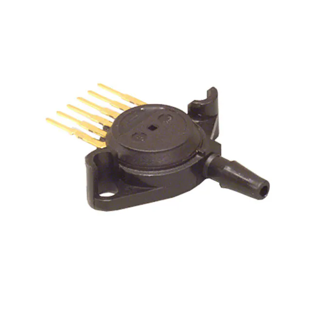
MPX4250A, MPXA4250A
20 to 250 kPa, Manifold absolute pressure sensor, on-chip
signal conditioned, temperature compensated and calibrated
Rev. 8.0 — 25 July 2017
1
Data sheet: technical data
General description
The MPX4250A/MPXA4250A Manifold Absolute Pressure (MAP) sensor for engine
control is designed to sense absolute air pressure within the intake manifold. This
measurement can be used to compute the amount of fuel required for each cylinder.
The MPX4250A/MPXA4250A piezoresistive transducer is a state-of-the-art monolithic
silicon pressure sensor designed for a wide range of applications, particularly those
employing a microcontroller or microprocessor with A/D inputs. This transducer combines
advanced micromachining techniques, thin-film metallization, and bipolar processing to
provide an accurate, high-level analog output signal that is proportional to the applied
pressure. The small form factor and high reliability of on-chip integration make the NXP
sensor a logical and economical choice for the automotive system engineer.
2
Features
• 1.5 % maximum error over 0 °C to 85 °C
• Specifically designed for intake manifold absolute pressure sensing in engine control
systems
• Patented silicon shear stress strain gauge
• Temperature compensated over –40 °C to +125 °C
• Offers reduction in weight and volume compared to existing hybrid modules
• Durable epoxy unibody element or thermoplastic small outline, surface mount package
• Ideal for non-automotive applications
• Available in three small outline packages and two unibody packages
MPXA4250A6U
98ASB17756C
CASE 482-01
MPXA4250AC6U/C6T1
98ASB17757C
CASE 482A-01
MPX4250A
98ASB42793B
CASE 867-08
Figure 1. Small outline and unibody packages
3
Typical applications
• Turbo boost engine control
• Ideally suited for microprocessor or microcontroller-based systems
MPX4250AP
98ASB42796B
CASE 867B-04
�MPX4250A, MPXA4250A
NXP Semiconductors
20 to 250 kPa, Manifold absolute pressure sensor, on-chip signal conditioned, temperature
compensated and calibrated
4
Ordering information
Table 1. Ordering information
Device name
Package
Options
# of Ports
Package
Name
None
Single
Pressure type
Dual
Gauge
Differential
Device
marking
Absolute
Small outline package (MPXA4250A series)
MPXA4250A6U
Rail
98ASB17756C
MPXA4250AC6U
Rail
98ASB17757C
MPXA4250AC6T1
Tape and Reel
98ASB17757C
•
•
MPXA4250A
•
•
MPXA4250A
•
•
MPXA4250A
•
MPX4250A
•
MPX4250A
Unibody package (MPX4250A series)
MPX4250A
Tray
98ASB42793B
MPX4250AP
Tray
98ASB42796B
5
•
•
Block diagram
VCC
2 (Small outline package)
3 (Unibody)
Sensing
Element
Gain Stage #2
and Ground
Reference
Shift
Circuitry
Thin Film
Temperature
Compensation
and
Gain Stage #1
2 (Unibody)
GND 3 (Small outline package)
VOUT
1 (Unibody)
4 (Small outline package)
Pins 4, 5 and 6 are NO CONNECTS
for unibody package devices.
Pins 1, 5, 6, 7, and 8 are NO CONNECTS
for small outline package devices.
Figure 2. Block diagram
6
Pinning information
6.1 Pinning
MPX4250A
(unibody)
5
DNC
1
5
DNC
VCC
2
6
DNC
GND
3
7
DNC
VOUT
4
8
DNC
6
DNC
4
DNC
VCC
GND
VOUT
3
DNC
2
1
MPXA4250A
(SOP)
Figure 3. Pinning diagram
MPx4250A
Data sheet: technical data
All information provided in this document is subject to legal disclaimers.
Rev. 8.0 — 25 July 2017
© NXP B.V. 2017. All rights reserved.
2 / 16
�MPX4250A, MPXA4250A
NXP Semiconductors
20 to 250 kPa, Manifold absolute pressure sensor, on-chip signal conditioned, temperature
compensated and calibrated
6.2 Pin description
Table 2. Pin descriptions — Unibody package
Symbol
Pin
Description
VOUT
1
Output voltage
GND
2
Ground
VCC
3
Voltage supply
DNC
4
Do not connect to external circuitry or ground
DNC
5
Do not connect to external circuitry or ground
DNC
6
Do not connect to external circuitry or ground
Table 3. Pin descriptions — Small outline package
Symbol
7
Pin
Description
DNC
1
Do no connect to external circuitry or ground
VCC
2
Voltage supply
GND
3
Ground
VOUT
4
Output voltage
DNC
5
Do not connect to external circuitry or ground
DNC
6
Do not connect to external circuitry or ground
DNC
7
Do not connect to external circuitry or ground
DNC
8
Do not connect to external circuitry or ground
Mechanical and electrical specifications
7.1 Maximum ratings
Table 4. Maximum ratings
TA = 25 °C unless otherwise noted. Exposure beyond the specified limits may cause permanent
damage or degradation to the device.
Rating
Symbol
Value
Unit
Maximum pressure (P1 > P2)
PMAX
1000
kPa
Storage temperature
TSTG
–40 to +125
°C
TA
–40 to +125
°C
Operating temperature
Figure 2 shows a block diagram of the internal circuitry integrated on a pressure sensor
chip.
MPx4250A
Data sheet: technical data
All information provided in this document is subject to legal disclaimers.
Rev. 8.0 — 25 July 2017
© NXP B.V. 2017. All rights reserved.
3 / 16
�MPX4250A, MPXA4250A
NXP Semiconductors
20 to 250 kPa, Manifold absolute pressure sensor, on-chip signal conditioned, temperature
compensated and calibrated
7.2 Operating characteristics
Table 5. Operating characteristics
(VCC = 5.1 Vdc, TA = 25 °C unless otherwise noted, P1 > P2. Decoupling circuit shown in Figure 5
required to meet electrical specifications.)
Symbol
POP
Supply voltage
Io
Supply current
[8]
[9]
8
[2]
[3]
Minimum pressure offset
[4]
Full scale output
VFSS
[5]
Full scale span
[6]
—
Accuracy
ΔV/ΔP
Sensitivity
(0 °C to 85 °C)
(0 °C to 85 °C)
(0 °C to 85 °C)
(0 °C to 85 °C)
[7]
Min
Typ
Max
Unit
20
—
250
kPa
4.85
5.1
5.35
Vdc
—
7.0
10
mAdc
0.133
0.204
0.274
Vdc
4.826
4.896
4.966
Vdc
—
4.692
—
Vdc
—
—
±1.5
%VFSS
—
20
—-
mV/kPa
tR
Response time
—
1.0
—-
ms
Io+
Output source current at full scale output
—
[7]
[1]
VFSO
—
[6]
Pressure range
VCC
Voff
[1]
[2]
[3]
[4]
[5]
Characteristic
—
0.1
—-
mAdc
[8]
—
20
—-
ms
[9]
—
± 0.5
—-
%VFSS
Warm-up time
Offset stability
1.0 kPa (kiloPascal) equals 0.145 psi.
Device is ratiometric within this specified excitation range.
Offset (Voff) is defined as the output voltage at the minimum rated pressure.
Full scale output (VFSO) is defined as the output voltage at the maximum or full rated pressure.
Full scale span (VFSS) is defined as the algebraic difference between the output voltage at full rated pressure and the
output voltage at the minimum rated pressure.
Accuracy (error budget) consists of the following:
• Linearity: Output deviation from a straight line relationship with pressure over the specified pressure range.
• Temperature hysteresis: Output deviation at any temperature within the operating temperature range, after the
temperature is cycled to and from the minimum or maximum operating temperature points, with zero pressure applied.
• Pressure hysteresis: Output deviation at any pressure within the specified range, when this pressure is cycled to and
from the minimum or maximum rated pressure, at 25 °C.
• TcSpan: Output deviation over the temperature range of 0 °C to 85 °C, relative to 25 °C.
• TcOffset: Output deviation with minimum rated pressure applied, over the temperature range of 0 °C to 85 °C, relative
to 25 °C.
Variation from nominal: The variation from nominal values, for offset or full scale span, as a percent of VFSS, at 25 °C.
Response time is defined as the time for the incremental change in the output to go from 10 % to 90 % of its final value
when subjected to a specified step change in pressure.
Warm-up time is defined as the time required for the product to meet the specified output voltage after the pressure has
been stabilized.
Offset stability is the product's output deviation when subjected to 1000 hours of pulsed pressure, temperature cycling
with bias test.
On-chip temperature compensation and calibration
Figure 4 illustrates the absolute pressure sensing chip in the basic chip carrier
(98ASB42793B). A fluorosilicone gel isolates the die surface and wire bonds from
the environment, while allowing the pressure signal to be transmitted to the sensor
diaphragm.
The MPX4250A/MPXA4250A pressure sensor operating characteristics and internal
reliability and qualification tests are based on use of dry air as the pressure media.
Media, other than dry air, may have adverse effects on sensor performance and long-
MPx4250A
Data sheet: technical data
All information provided in this document is subject to legal disclaimers.
Rev. 8.0 — 25 July 2017
© NXP B.V. 2017. All rights reserved.
4 / 16
�MPX4250A, MPXA4250A
NXP Semiconductors
20 to 250 kPa, Manifold absolute pressure sensor, on-chip signal conditioned, temperature
compensated and calibrated
term reliability. Contact the factory for information regarding media compatibility in your
application.
Figure 5 shows the recommended decoupling circuit for interfacing the output of the
integrated sensor to the A/D input of a microprocessor or microcontroller.
Figure 6 shows the sensor output signal relative to pressure input. Typical, minimum, and
maximum output curves are shown for operation over a temperature range of 0 °C to 85
°C using the decoupling circuit shown in Figure 5. The output will saturate outside of the
specified pressure range.
Fluoro silicone
die coat
Stainless steel
metal cover
Die
P1
Wire bond
Epoxy case
RTV die bond
Lead frame
Sealed vacuum reference
Figure 4. Cross sectional diagram (not to scale)
+5.1 V
Output
Vout
VCC
IPS
1.0 µF
GND
0.01 µF
470 pF
For additional output filtering, please refer to Application Note AN1646
Figure 5. Recommended power supply decoupling and output filtering
5.0
4.5
4.0
Output (Volts)
3.5
Transfer Function:
Vout = VCC x (P x 0.004 – 0.04) ± Error
VCC = 5.1 Vdc
Temperature = 0 °C to 85 °C
TYP
3.0
2.5
MAX
2.0
1.5
MIN
1.0
0.5
0
10
20
30
40
50
60
70
80
90
0
100
110
120
130
140
150
160
170
180
190
200
210
220
230
240
250
260
0
Pressure in kPa
Figure 6. Output versus absolute pressure
MPx4250A
Data sheet: technical data
All information provided in this document is subject to legal disclaimers.
Rev. 8.0 — 25 July 2017
© NXP B.V. 2017. All rights reserved.
5 / 16
�MPX4250A, MPXA4250A
NXP Semiconductors
20 to 250 kPa, Manifold absolute pressure sensor, on-chip signal conditioned, temperature
compensated and calibrated
Nominal transfer value:
VOUT = VCC x (P × 0.004 – 0.04) ± (Pressure error × Temp. Factor × 0.004 x V CC )
VCC = 5.1 ± 0.25 Vdc
Figure 7. Transfer function
4.0
Temp °C Multiplier
3.0
Temperature
error
factor
2.0
–40
0 to 85
3
1
+125
3
1.0
0.0
–40
–20
0
20
40
60
80
100
120
140
Temperature in °C
Note: The temperature multiplier is a linear response from 0°C to –40°C and from 85°C to 125°C.
Figure 8. Temperature error band
Figure 9. Pressure error band
9
Package information
9.1 Minimum recommended footprint for surface mounted applications
Surface mount board layout is a critical portion of the total design. The footprint for the
surface mount packages must be the correct size to ensure proper solder connection
interface between the board and the package. With the correct Footprint, the packages
will self align when subjected to a solder reflow process. It is always recommended to
design boards with a solder mask layer to avoid bridging and shorting between solder
pads.
MPx4250A
Data sheet: technical data
All information provided in this document is subject to legal disclaimers.
Rev. 8.0 — 25 July 2017
© NXP B.V. 2017. All rights reserved.
6 / 16
�MPX4250A, MPXA4250A
NXP Semiconductors
20 to 250 kPa, Manifold absolute pressure sensor, on-chip signal conditioned, temperature
compensated and calibrated
0.100 TYP 8X
2.54
0.660
16.76
0.060 TYP 8X
1.52
0.300
7.62
0.100 TYP 8X
2.54
inch
mm
SCALE 2:1
Figure 10. SOP footprint (Case 482)
MPx4250A
Data sheet: technical data
All information provided in this document is subject to legal disclaimers.
Rev. 8.0 — 25 July 2017
© NXP B.V. 2017. All rights reserved.
7 / 16
�MPX4250A, MPXA4250A
NXP Semiconductors
20 to 250 kPa, Manifold absolute pressure sensor, on-chip signal conditioned, temperature
compensated and calibrated
9.2 Package description
Figure 11. Package name 98ASB15576C, Case 482-01 Issue O, Small outline package
MPx4250A
Data sheet: technical data
All information provided in this document is subject to legal disclaimers.
Rev. 8.0 — 25 July 2017
© NXP B.V. 2017. All rights reserved.
8 / 16
�MPX4250A, MPXA4250A
NXP Semiconductors
20 to 250 kPa, Manifold absolute pressure sensor, on-chip signal conditioned, temperature
compensated and calibrated
–A–
D 8 PL
4
0.25 (0.010)
5
M
T B
S
A
NOTES:
1. DIMENSIONING AND TOLERANCING PER ANSI
Y14.5M, 1982.
2. CONTROLLING DIMENSION: INCH.
3. DIMENSION A AND B DO NOT INCLUDE MOLD
PROTRUSION.
4. MAXIMUM MOLD PROTRUSION 0.15 (0.006).
5. ALL VERTICAL SURFACES 5 TYPICAL DRAFT.
S
N –B–
G
8
1
S
DIM
A
B
C
D
G
H
J
K
M
N
S
V
W
W
V
C
H
J
INCHES
MIN
MAX
0.415
0.425
0.415
0.425
0.500
0.520
0.038
0.042
0.100 BSC
0.002
0.010
0.009
0.011
0.061
0.071
0
7
0.444
0.448
0.709
0.725
0.245
0.255
0.115
0.125
MILLIMETERS
MIN
MAX
10.54
10.79
10.54
10.79
12.70
13.21
0.96
1.07
2.54 BSC
0.05
0.25
0.23
0.28
1.55
1.80
0
7
11.28
11.38
18.01
18.41
6.22
6.48
2.92
3.17
–T–
M
K
PIN 1 IDENTIFIER
SEATING
PLANE
Figure 12. Package name 98ASB17757C, Case 482A-01, Issue A, small outline package
Figure 13. Package name 98ASB42793B, Case 867-08, Issue N, unibody package
MPx4250A
Data sheet: technical data
All information provided in this document is subject to legal disclaimers.
Rev. 8.0 — 25 July 2017
© NXP B.V. 2017. All rights reserved.
9 / 16
�NXP Semiconductors
MPX4250A, MPXA4250A
20 to 250 kPa, Manifold absolute pressure sensor, on-chip signal conditioned, temperature
compensated and calibrated
MPx4250A
Data sheet: technical data
All information provided in this document is subject to legal disclaimers.
Rev. 8.0 — 25 July 2017
© NXP B.V. 2017. All rights reserved.
10 / 16
�NXP Semiconductors
MPX4250A, MPXA4250A
20 to 250 kPa, Manifold absolute pressure sensor, on-chip signal conditioned, temperature
compensated and calibrated
Figure 14. Package name 98ASB42796B, Case 867B-04, Issue J
MPx4250A
Data sheet: technical data
All information provided in this document is subject to legal disclaimers.
Rev. 8.0 — 25 July 2017
© NXP B.V. 2017. All rights reserved.
11 / 16
�MPX4250A, MPXA4250A
NXP Semiconductors
20 to 250 kPa, Manifold absolute pressure sensor, on-chip signal conditioned, temperature
compensated and calibrated
10 Revision history
Table 6. Revision history
Document ID
Release date
Data sheet status
Change notice
Supercedes
MPX4250A v.8.0
20170725
Technical data
—
MPX4250A v.7.0
Modifications:
• The format of this data sheet has been redesigned to comply with the new identity guidelines of
NXP Semiconductors.
• Legal texts have been adapted to the new company name where appropriate.
• Updated the document title from "Integrated Silicon Pressure Sensor On-Chip Signal
Conditioned, Temperature Compensated and Calibrated" to "0 to 250 kPa, Differential, gauge
pressure sensor, on-chip signal conditioned, temperature compensated."
• Added Figure 1 "Small outline and unibody packages" in Section 2 "Features".
• Updated Table 1 "Ordering information" in Section 4 "Ordering information".
• Revised Figure 2 "Block diagram " in Section 5 "Block diagram" as follows:
– Changed VS to VCC
• Added pinning illustration as Figure 3 "Pinning diagram" in Section 6.1
• Added pin descriptions in Table 2 "Pin descriptions — Unibody package" and Table 3 "Pin
descriptions — Small outline package" in Section 6.2.
• Changed VS to VCC in the description and within the body of Table 5 "Operating characteristics"
in Section 7.2 "Operating characteristics".
• Updated the figures in Section 8 "On-chip temperature compensation and calibration" as
follows:
– Figure 4 "Cross sectional diagram (not to scale)"
– Figure 5 "Recommended power supply decoupling and output filtering"
– Figure 6 "Output versus absolute pressure"
– Figure 7 "Transfer function"
– Figure 9 "Pressure error band"
• Updated the figures and figure titles in Section 9.2 "Package description" as follows:
– Figure 11 "Package name 98ASB15576C, Case 482-01 Issue O, Small outline package"
– Figure 12 "Package name 98ASB17757C, Case 482A-01, Issue A, small outline package"
– Figure 13 "Package name 98ASB42793B, Case 867-08, Issue N, unibody package"
– Figure 14 "Package name 98ASB42796B, Case 867B-04, Issue J"
MPX4250A v.7.0
20090131
MPx4250A
Data sheet: technical data
Technical data
—
All information provided in this document is subject to legal disclaimers.
Rev. 8.0 — 25 July 2017
MPX4250A v.6.0
© NXP B.V. 2017. All rights reserved.
12 / 16
�MPX4250A, MPXA4250A
NXP Semiconductors
20 to 250 kPa, Manifold absolute pressure sensor, on-chip signal conditioned, temperature
compensated and calibrated
11 Legal information
11.1 Data sheet status
Document status
[1][2]
Product status
[3]
Definition
[short] Data sheet: product_preview
Development
This document contains certain information on a product under development.
NXP reserves the right to change or discontinue this product without notice.
{short] Data sheet: advance information
Qualification
This document contains information on a new product. Specifications and
information herein are subject to change without notice.
[short] Data sheet: technical data
Production
This document contains the product specification. NXP Semiconductors
reserves the right to change the detail specifications as may be required to
permit improvements in the design of its products.
[1]
[2]
[3]
Please consult the most recently issued document before initiating or completing a design.
The term 'short data sheet' is explained in section "Definitions".
The product status of device(s) described in this document may have changed since this document was published and may differ in case of multiple
devices. The latest product status information is available on the Internet at URL http://www.nxp.com.
limitation specifications and product descriptions, at any time and without
notice. This document supersedes and replaces all information supplied prior
to the publication hereof.
11.2 Definitions
Draft — The document is a draft version only. The content is still under
internal review and subject to formal approval, which may result in
modifications or additions. NXP Semiconductors does not give any
representations or warranties as to the accuracy or completeness of
information included herein and shall have no liability for the consequences
of use of such information.
Short data sheet — A short data sheet is an extract from a full data sheet
with the same product type number(s) and title. A short data sheet is
intended for quick reference only and should not be relied upon to contain
detailed and full information. For detailed and full information see the
relevant full data sheet, which is available on request via the local NXP
Semiconductors sales office. In case of any inconsistency or conflict with the
short data sheet, the full data sheet shall prevail.
Product specification — The information and data provided in a
technical data data sheet shall define the specification of the product as
agreed between NXP Semiconductors and its customer, unless NXP
Semiconductors and customer have explicitly agreed otherwise in writing.
In no event however, shall an agreement be valid in which the NXP
Semiconductors product is deemed to offer functions and qualities beyond
those described in the technical data data sheet.
11.3 Disclaimers
Limited warranty and liability — Information in this document is believed
to be accurate and reliable. However, NXP Semiconductors does not
give any representations or warranties, expressed or implied, as to the
accuracy or completeness of such information and shall have no liability
for the consequences of use of such information. NXP Semiconductors
takes no responsibility for the content in this document if provided by an
information source outside of NXP Semiconductors. In no event shall NXP
Semiconductors be liable for any indirect, incidental, punitive, special or
consequential damages (including - without limitation - lost profits, lost
savings, business interruption, costs related to the removal or replacement
of any products or rework charges) whether or not such damages are based
on tort (including negligence), warranty, breach of contract or any other
legal theory. Notwithstanding any damages that customer might incur for
any reason whatsoever, NXP Semiconductors’ aggregate and cumulative
liability towards customer for the products described herein shall be limited
in accordance with the Terms and conditions of commercial sale of NXP
Semiconductors.
Right to make changes — NXP Semiconductors reserves the right to
make changes to information published in this document, including without
MPx4250A
Data sheet: technical data
Applications — Applications that are described herein for any of these
products are for illustrative purposes only. NXP Semiconductors makes
no representation or warranty that such applications will be suitable
for the specified use without further testing or modification. Customers
are responsible for the design and operation of their applications and
products using NXP Semiconductors products, and NXP Semiconductors
accepts no liability for any assistance with applications or customer product
design. It is customer’s sole responsibility to determine whether the NXP
Semiconductors product is suitable and fit for the customer’s applications
and products planned, as well as for the planned application and use of
customer’s third party customer(s). Customers should provide appropriate
design and operating safeguards to minimize the risks associated with
their applications and products. NXP Semiconductors does not accept any
liability related to any default, damage, costs or problem which is based
on any weakness or default in the customer’s applications or products, or
the application or use by customer’s third party customer(s). Customer is
responsible for doing all necessary testing for the customer’s applications
and products using NXP Semiconductors products in order to avoid a
default of the applications and the products or of the application or use by
customer’s third party customer(s). NXP does not accept any liability in this
respect.
Limiting values — Stress above one or more limiting values (as defined in
the Absolute Maximum Ratings System of IEC 60134) will cause permanent
damage to the device. Limiting values are stress ratings only and (proper)
operation of the device at these or any other conditions above those
given in the Recommended operating conditions section (if present) or the
Characteristics sections of this document is not warranted. Constant or
repeated exposure to limiting values will permanently and irreversibly affect
the quality and reliability of the device.
Terms and conditions of commercial sale — NXP Semiconductors
products are sold subject to the general terms and conditions of commercial
sale, as published at http://www.nxp.com/profile/terms, unless otherwise
agreed in a valid written individual agreement. In case an individual
agreement is concluded only the terms and conditions of the respective
agreement shall apply. NXP Semiconductors hereby expressly objects to
applying the customer’s general terms and conditions with regard to the
purchase of NXP Semiconductors products by customer.
No offer to sell or license — Nothing in this document may be interpreted
or construed as an offer to sell products that is open for acceptance or
the grant, conveyance or implication of any license under any copyrights,
patents or other industrial or intellectual property rights.
Suitability for use in automotive applications — This NXP
Semiconductors product has been qualified for use in automotive
All information provided in this document is subject to legal disclaimers.
Rev. 8.0 — 25 July 2017
© NXP B.V. 2017. All rights reserved.
13 / 16
�MPX4250A, MPXA4250A
NXP Semiconductors
20 to 250 kPa, Manifold absolute pressure sensor, on-chip signal conditioned, temperature
compensated and calibrated
applications. Unless otherwise agreed in writing, the product is not designed,
authorized or warranted to be suitable for use in life support, life-critical or
safety-critical systems or equipment, nor in applications where failure or
malfunction of an NXP Semiconductors product can reasonably be expected
to result in personal injury, death or severe property or environmental
damage. NXP Semiconductors and its suppliers accept no liability for
inclusion and/or use of NXP Semiconductors products in such equipment or
applications and therefore such inclusion and/or use is at the customer's own
risk.
Export control — This document as well as the item(s) described herein
may be subject to export control regulations. Export might require a prior
authorization from competent authorities.
MPx4250A
Data sheet: technical data
Translations — A non-English (translated) version of a document is for
reference only. The English version shall prevail in case of any discrepancy
between the translated and English versions.
11.4 Trademarks
Notice: All referenced brands, product names, service names and
trademarks are the property of their respective owners.
Freescale — is a trademark of NXP B.V.
NXP — is a trademark of NXP B.V.
All information provided in this document is subject to legal disclaimers.
Rev. 8.0 — 25 July 2017
© NXP B.V. 2017. All rights reserved.
14 / 16
�MPX4250A, MPXA4250A
NXP Semiconductors
20 to 250 kPa, Manifold absolute pressure sensor, on-chip signal conditioned, temperature
compensated and calibrated
Tables
Tab. 1.
Tab. 2.
Tab. 3.
Ordering information ..........................................2
Pin descriptions — Unibody package ................3
Pin descriptions — Small outline package ........ 3
Tab. 4.
Tab. 5.
Tab. 6.
Maximum ratings ...............................................3
Operating characteristics ...................................4
Revision history ...............................................12
Fig. 10.
Fig. 11.
SOP footprint (Case 482) ..................................7
Package name 98ASB15576C, Case
482-01 Issue O, Small outline package .............8
Package name 98ASB17757C, Case
482A-01, Issue A, small outline package .......... 9
Package name 98ASB42793B, Case
867-08, Issue N, unibody package ....................9
Package name 98ASB42796B, Case
867B-04, Issue J ............................................. 10
Figures
Fig. 1.
Fig. 2.
Fig. 3.
Fig. 4.
Fig. 5.
Fig. 6.
Fig. 7.
Fig. 8.
Fig. 9.
Small outline and unibody packages .................1
Block diagram ................................................... 2
Pinning diagram ................................................ 2
Cross sectional diagram (not to scale) .............. 5
Recommended power supply decoupling
and output filtering ............................................ 5
Output versus absolute pressure ...................... 5
Transfer function ............................................... 6
Temperature error band .................................... 6
Pressure error band .......................................... 6
MPx4250A
Data sheet: technical data
Fig. 12.
Fig. 13.
Fig. 14.
All information provided in this document is subject to legal disclaimers.
Rev. 8.0 — 25 July 2017
© NXP B.V. 2017. All rights reserved.
15 / 16
�NXP Semiconductors
MPX4250A, MPXA4250A
20 to 250 kPa, Manifold absolute pressure sensor, on-chip signal conditioned, temperature
compensated and calibrated
Contents
1
2
3
4
5
6
6.1
6.2
7
7.1
7.2
8
9
9.1
9.2
10
11
General description ............................................ 1
Features ............................................................... 1
Typical applications ............................................1
Ordering information .......................................... 2
Block diagram ..................................................... 2
Pinning information ............................................ 2
Pinning ............................................................... 2
Pin description ................................................... 3
Mechanical and electrical specifications .......... 3
Maximum ratings ............................................... 3
Operating characteristics ................................... 4
On-chip temperature compensation and
calibration ............................................................ 4
Package information ...........................................6
Minimum recommended footprint for surface
mounted applications .........................................6
Package description .......................................... 8
Revision history ................................................ 12
Legal information .............................................. 13
Please be aware that important notices concerning this document and the product(s)
described herein, have been included in section 'Legal information'.
© NXP B.V. 2017.
All rights reserved.
For more information, please visit: http://www.nxp.com
For sales office addresses, please send an email to: salesaddresses@nxp.com
Date of release: 25 July 2017
Document identifier: MPx4250A
�