NXP Semiconductors
Data Sheet: Technical Data
Document Number: MPXH6400A
Rev. 6, 03/2017
MPXH6400A, 20 to 400 kPa, Absolute,
Integrated Pressure Sensor
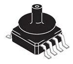
MPXH6400A
The NXP MPXxx6400A series sensor integrates on-chip, bipolar op amp circuitry
and thin film resistor networks to provide a high output signal and temperature
compensation. The small form factor and high reliability of on-chip integration
make this pressure sensor a logical and economical choice for the system
designer.
The MPXxx6400A series piezoresistive transducer is a state-of-the-art,
monolithic, signal conditioned, silicon pressure sensor. This sensor combines
advanced micromachining techniques, thin film metallization, and bipolar
semiconductor processing to provide an accurate, high level analog output signal
that is proportional to applied pressure.
Features
Super small outline package
MPXHZ6400A6T1 MPXH6400AC6U/6T1/
Case 98ARH99066A MPXHZ6400AC6T1
Case 98ARH99089A
•
Improved accuracy at high temperature
•
Available in super small outline package
•
1.5% maximum error over 0 °C to 85 °C
•
Fully calibrated and compensated
•
Ideally suited for microprocessor or microcontroller-based systems
DNC 5
•
Temperature compensated from -40 °C to +125 °C
4 VOUT
DNC 6
3 GND
•
Durable thermoplastic surface mount package
•
Package porting and mounting options enable tube attachment for liquefied
natural gas (LPG) or remote sensing applications
DNC 7
DNC 8
2 VS
1 DNC
Top view
Typical applications
•
Fuel injected car engines
•
Vehicles powered by green gases (for example LPG and CNG)
•
Small engines
•
Industrial controls
Pin 1 identification,
chamfered corner.
Pinout
Ordering information
Part number
Shipping
Package
# of Ports
None
Single
Pressure type
Dual
Gauge
Differential
Absolute
Device
marking
•
MPXH6400A
Super Small Outline Package (Media resistant gel)
MPXH6400AC6U
Rail
98ARH99089A
MPXH6400AC6T1
Tape and Reel
98ARH99089A
MPXHZ6400A6T1
Tape and Reel
98ARH99066A
MPXHZ6400AC6T1
Tape and Reel
98ARH99089A
•
•
•
•
NXP reserves the right to change the detail specifications as may be required to permit
improvements in the design of its products.
© NXP B.V. 2017
•
MPXH6400A
•
MPXHZ6400A
•
MPXHZ6400A
�Contents
1
2
3
4
5
General Description . . . . . . . . . . . . . . . . . . . . . . . . . . . . . . . . . . . . . . . . . . . . . . . . . . . . . . . . . . . . . . . . . . . . . . . . . . . . . . 3
1.1 Block diagram . . . . . . . . . . . . . . . . . . . . . . . . . . . . . . . . . . . . . . . . . . . . . . . . . . . . . . . . . . . . . . . . . . . . . . . . . . . . . . . 3
1.2 Pinout . . . . . . . . . . . . . . . . . . . . . . . . . . . . . . . . . . . . . . . . . . . . . . . . . . . . . . . . . . . . . . . . . . . . . . . . . . . . . . . . . . . . . 3
Mechanical and Electrical Specifications. . . . . . . . . . . . . . . . . . . . . . . . . . . . . . . . . . . . . . . . . . . . . . . . . . . . . . . . . . . . . 4
2.1 Maximum ratings. . . . . . . . . . . . . . . . . . . . . . . . . . . . . . . . . . . . . . . . . . . . . . . . . . . . . . . . . . . . . . . . . . . . . . . . . . . . . 4
2.2 Operating characteristics . . . . . . . . . . . . . . . . . . . . . . . . . . . . . . . . . . . . . . . . . . . . . . . . . . . . . . . . . . . . . . . . . . . . . . 4
On-chip Temperature Compensation and Calibration . . . . . . . . . . . . . . . . . . . . . . . . . . . . . . . . . . . . . . . . . . . . . . . . . . 5
Package Information. . . . . . . . . . . . . . . . . . . . . . . . . . . . . . . . . . . . . . . . . . . . . . . . . . . . . . . . . . . . . . . . . . . . . . . . . . . . . . 8
4.1 Minimum recommended footprint for surface mounted applications . . . . . . . . . . . . . . . . . . . . . . . . . . . . . . . . . . . . . 8
4.2 Package Dimensions . . . . . . . . . . . . . . . . . . . . . . . . . . . . . . . . . . . . . . . . . . . . . . . . . . . . . . . . . . . . . . . . . . . . . . . . . 9
Revision History . . . . . . . . . . . . . . . . . . . . . . . . . . . . . . . . . . . . . . . . . . . . . . . . . . . . . . . . . . . . . . . . . . . . . . . . . . . . . . . . 14
Related Documentation
The MPXxx6400A device features and operations are described in a variety of reference manuals, user guides, and application
notes. To find the most-current versions of these documents:
1.
2.
Go to the MPXx6400 web page at http://www.nxp.com/products/:MPXx6400.
Click the Documentation tab.
MPXH6400A
2
Sensors
NXP B.V.
�1
General Description
1.1
Block diagram
Figure 1 shows a block diagram of the internal circuitry integrated on a pressure sensor chip.
VS
Thin Film
Temperature
Compensation
and Gain
Stage #1
Sensing
Element
GND
Gain Stage #2
and
Ground
Reference
Shift Circuitry
VOUT
Pins 1, 5, 6, 7, and 8 are internal device connections.
Do not connect to external circuitry or ground.
Figure 1. Integrated pressure sensor block diagram
1.2
Pinout
DNC 5
4 VOUT
DNC 6
3 GND
DNC 7
DNC 8
2 VS
1 DNC
Pin 1 identification,
chamfered corner.
Figure 2. Device pinout (top view)
Table 1. Pin functions
Pin
Name
1
DNC
Function
Do not connect to external circuitry or ground. Pin 1 is notated by chamfered corner.
Voltage supply
2
VS
3
GND
Ground
4
VOUT
Output voltage
5
DNC
Do not connect to external circuitry or ground.
6
DNC
Do not connect to external circuitry or ground.
7
DNC
Do not connect to external circuitry or ground.
8
DNC
Do not connect to external circuitry or ground.
MPXH6400A
Sensors
NXP B.V.
3
�2
Mechanical and Electrical Specifications
2.1
Maximum ratings
Table 2. Maximum ratings(1)
Parametrics
Symbol
Value
Units
Maximum pressure (P1 > P2)
PMAX
1600
kPa
Storage temperature
TSTG
-40° to +125°
°C
TA
-40° to +125°
°C
IO +
0.5
mAdc
IO -
-0.5
mAdc
Operating temperature
Output source current @ full-scale output(2)
Output sink current @ minimum pressure
offset(2)
1.Exposure beyond the specified limits may cause permanent damage or degradation to the device.
2.Maximum output current is controlled by effective impedance from VOUT to GND or VOUT to VS in the application circuit.
2.2
Operating characteristics
Table 3. Operating characteristics (VS = 5.0 VDC, TA = 25 °C unless otherwise noted, P1 > P2.)
Characteristic
Pressure range
Symbol
Min
Typ
Max
Unit
POP
20
—
400
kPa
Supply voltage(1)
VS
4.64
5.0
5.36
VDC
Supply current
IO
—
6.0
10
mAdc
Minimum pressure offset(2) (0 to 85 °C) @ VS = 5.0 Volts
VOFF
0.133
0.2
0.267
VDC
Full-scale output(3) (0 to 85 °C) @ VS = 5.0 Volts
VFSO
4.733
4.8
4.866
VDC
Full-scale span(4) (0 to 85 °C) @ VS = 5.0 Volts
VFSS
4.467
4.6
4.733
VDC
—
—
—
±1.5
%VFSS
Accuracy(5) (0 to 85 °C)
Sensitivity
V/P
—
12.1
—
mV/kPa
Response time(6)
tR
—
1.0
—
ms
Warm-up time(7)
—
—
20
—
ms
Offset stability(8)
—
—
±0.25
—
%VFSS
1.Device is ratiometric within this specified excitation range.
2.Offset (VOFF) is defined as the output voltage at the minimum rated pressure.
3.Full-scale output (VFSO) is defined as the output voltage at the maximum or full-rated pressure.
4.Full-scale span (VFSS) is defined as the algebraic difference between the output voltage at full-rated pressure and the output voltage at the
minimum rated pressures
5.Accuracy is the deviation in actual output from nominal output over the entire pressure range and temperature range as a percent of span at
25 °C due to all sources of error including the following:
Linearity: Output deviation from a straight line relationship with pressure over the specified pressure range.
Temperature hysteresis:Output deviation at any temperature within the operating temperature range, after the temperature is cycled to
and from the minimum or maximum operating temperature points, with zero differential pressure applied.
Pressure hysteresis:
Output deviation at any pressure within the specified range, when this pressure is cycled to and from minimum
or maximum rated pressure at 25 °C
TcSpan: Output deviation over the temperature range of 0 to 85 °C, relative to 25 °C.
TcOffset: Output deviation with minimum rated pressure applied, over the temperature range of 0 to 85 °C, relative to 25 °C.
Variation from Nominal: The variation from nominal values, for offset or full-scale span, as a percent of VFSS, at 25 °C.
6.Response time is defined as the time for the incremental change in the output to go from 10% to 90% of its final value when subjected to a
specified step change in pressure.
7.Warm-up time is defined as the time required for the product to meet the specified output voltage after the pressure has been stabilized.
8.Offset stability is the product's output deviation when subjected to 1000 cycles of pulsed pressure, temperature cycling with bias test.
MPXH6400A
4
Sensors
NXP B.V.
�3
On-chip Temperature Compensation and Calibration
Figure 3 illustrates the absolute sensing chip in the basic super small outline chip carrier (case 98ARH99066A).
Figure 4 shows a typical application circuit (output source current operation).
Figure 5 shows the sensor output signal relative to pressure input. Typical minimum and maximum output curves are shown for
operation over 0 to 85 °C temperature range. The output will saturate outside of the rated pressure range.
A fluorosilicone gel isolates the die surface and wire bonds from the environment, while allowing the pressure signal to be
transmitted to the silicon diaphragm. The MPXH6400A/MPXHZ6400A pressure sensor operating characteristics, internal
reliability and qualification tests are based on use of dry air as the pressure media. Media other than dry air may have adverse
effects on sensor performance and long-term reliability. Contact the factory for information regarding media compatibility in your
application.
Fluorosilicone
Gel Die Coat
Die
Stainless
Steel Cap
P1
Thermoplastic
Case
Wire
Bond
Lead
Frame
Absolute
Die Bond
Sealed Vacuum
Reference
Figure 3. Cross-sectional diagram (not-to-scale)
+5.1 V
VS
VOUT
100 nF
To ADC
1 μF
GND
47 pF
51 K
Figure 4. Recommended power supply decoupling and output filtering
MPXH6400A
Sensors
NXP B.V.
5
�5.0
4.5
4.0
Output (Volts)
3.5
Transfer Function:
VOUT = VS x (0.002421xP–0.00842 ± Error
VS = 5.0 VDC
Temperature = 0 to 85 °C
3.0
MAX
2.5
2.0
TYP
1.5
1.0
MIN
0
20
40
60
80
100
120
140
160
180
200
220
240
260
280
300
320
340
360
380
400
0.5
Pressure (Reference to Sealed Vacuum) in kPa
Figure 5. Output vs. absolute pressure
Normal Transfer Value: VOUT = VS x (0.002421 x P – 0.00842)
± Pressure Error x Temp. Factor x 0.002421 x VS
VS = 5.0 ± 0.36 VDC
Figure 6. Transfer function
Temperature Error Factor
4.0
3.0
Break Points
2.0
1.0
Temp
0.0
-40
-20
0
20
80
40
60
Temperature in °C
100
120
NOTE: The Temperature Multiplier is a linear response from 0 °C to -40 °C and from 85 °C to 125 °C
140
- 40
0 to 85
125
Multiplier
3
1
1.75
Figure 7. Temperature error band
MPXH6400A
6
Sensors
NXP B.V.
�Error Limits for Pressure
±5.5 (kPa)
6.0
5.0
4.0
Pressure Error (kPa)
3.0
2.0
1.0
0.0
-1.0
20 40 60 80 100 120 140 160 180 200 220 240 260 280 300 320 340 360 380 400
-2.0
-3.0
-4.0
- 5.0
Pressure (in kPa)
- 6.0
Pressure
20 to 400 (kPa)
Error (Max)
±5.5 (kPa)
Figure 8. Pressure error band
MPXH6400A
Sensors
NXP B.V.
7
�4
Package Information
4.1
Minimum recommended footprint for surface mounted applications
Surface mount board layout is a critical portion of the total design. The footprint for the semiconductor package must be the
correct size to ensure proper solder connection interface between the board and the package. With the correct pad geometry,
the packages will self-align when subjected to a solder reflow process. It is always recommended to fabricate boards with a solder
mask layer to avoid bridging and/or shorting between solder pads, especially on tight tolerances and/or tight layouts.
0.050
1.27
TYP
0.387
9.83
0.150
3.81
0.027 TYP 8X
0.69
0.053 TYP 8X
1.35
inch
mm
Figure 9. SSOP footprint
MPXH6400A
8
Sensors
NXP B.V.
�4.2
Package Dimensions
This drawing is located at http://cache.nxp.com/assets/documents/data/en/package-information/98ARH99066A.pdf.
Case 98ARH99066A, super small outline package, surface mount
MPXH6400A
Sensors
NXP B.V.
9
�Case 98ARH99066A, super small outline package, surface mount
MPXH6400A
10
Sensors
NXP B.V.
�Case 98ARH99066A, super small outline package, surface mount
MPXH6400A
Sensors
NXP B.V.
11
�This drawing is located at http://cache.nxp.com/assets/documents/data/en/package-information/98ARH99089A.pdf.
Case 98ARH99089A, small outline package, surface mount
MPXH6400A
12
Sensors
NXP B.V.
�Case 98ARH99089A, small outline package, surface mount
MPXH6400A
Sensors
NXP B.V.
13
�5
Revision History
Table 4. Revision history
Document ID
Release Date
Data sheet status
Change notice
Supersedes
MPXH6400A Rev. 6
2017 March
Technical data
—
MPXH6400A Rev. 5.0
Modifications
• Revised VS = 10.0 VDC value to VS = 5.0 VDC in Table 3.
• The format of this data sheet has been redesigned to comply with current identity guidelines of NXP
Semiconductors. Legal texts have been adapted to the new company name where appropriate.
• Updated package outlines Section 4.2, “Package Dimensions” to comply with current identity guidelines of NXP
Semiconductors.
MPXH6400A Rev. 5.0
2015 September
Technical data
—
MPXH64-00A Rev.
MPXH6400A
14
Sensors
NXP B.V.
�How to Reach Us:
Information in this document is provided solely to enable system and software
Home Page:
NXP.com
implementers to use NXP products. There are no expressed or implied copyright
Web Support:
http://www.nxp.com/support
information in this document. NXP reserves the right to make changes without further
licenses granted hereunder to design or fabricate any integrated circuits based on the
notice to any products herein.
NXP makes no warranty, representation, or guarantee regarding the suitability of its
products for any particular purpose, nor does NXP assume any liability arising out of
the application or use of any product or circuit, and specifically disclaims any and all
liability, including without limitation, consequential or incidental damages. "Typical"
parameters that may be provided in NXP data sheets and/or specifications can and do
vary in different applications, and actual performance may vary over time. All operating
parameters, including "typicals," must be validated for each customer application by the
customer's technical experts. NXP does not convey any license under its patent rights
nor the rights of others. NXP sells products pursuant to standard terms and conditions
of sale, which can be found at the following address:
http://www.nxp.com/terms-of-use.html.
NXP, the NXP logo, Freescale, the Freescale logo, and the Energy Efficient Solutions
logo are trademarks of NXP B.V. All other product or service names are the property of
their respective owners. All rights reserved.
© NXP B.V. 2017.
Document Number: MPXH6400A
Rev. 6
03/2017
�