Freescale Semiconductor
Technical Data
RF Power Field Effect Transistors
N--Channel Enhancement--Mode Lateral MOSFETs
MRF21045LR3
MRF21045LSR3
LIFETIME BUY
Designed for W--CDMA base station applications with frequencies from 2110
to 2170 MHz. Suitable for TDMA, CDMA and multicarrier amplifier
applications. To be used in Class AB for PCN--PCS/cellular radio and WLL
applications.
• Typical 2--carrier W--CDMA Performance for VDD = 28 Volts, IDQ = 500 mA,
f = 2157.5 MHz, Channel Bandwidth = 3.84 MHz, Adjacent Channels
measured over 3.84 MHz Bandwidth at f1 --5 MHz and f2 +5 MHz,
Distortion Products measured over a 3.84 MHz Bandwidth at f1 --10 MHz
and f2 +10 MHz, Peak/Avg. = 8.3 dB @ 0.01% Probability on CCDF.
Output Power — 10 Watts Avg.
Efficiency — 23.5%
Gain — 15 dB
IM3 — --37.5 dBc
ACPR — --41 dBc
• Capable of Handling 5:1 VSWR, @ 28 Vdc, 2140 MHz, 45 Watts CW
Output Power
Features
• Internally Matched for Ease of Use
• High Gain, High Efficiency and High Linearity
• Integrated ESD Protection
• Designed for Maximum Gain and Insertion Phase Flatness
• Excellent Thermal Stability
• Characterized with Series Equivalent Large--Signal Impedance Parameters
• Low Gold Plating Thickness on Leads, 40μ″ Nominal.
• RoHS Compliant
• In Tape and Reel. R3 Suffix = 250 Units per 32 mm, 13 Inch Reel.
2110--2170 MHz, 45 W, 28 V
LATERAL N--CHANNEL
RF POWER MOSFETs
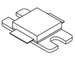
CASE 465E--04, STYLE 1
NI--400
MRF21045LR3
CASE 465F--04, STYLE 1
NI--400S
MRF21045LSR3
Table 1. Maximum Ratings
Rating
Symbol
Value
Unit
Drain--Source Voltage
VDSS
--0.5, +65
Vdc
Gate--Source Voltage
VGS
--0.5, +15
Vdc
Total Device Dissipation @ TC = 25°C
Derate above 25°C
PD
105
0.60
W
W/°C
Storage Temperature Range
Tstg
-- 65 to +150
°C
Case Operating Temperature
TC
150
°C
Operating Junction Temperature
TJ
200
°C
Symbol
Value (1)
Unit
RθJC
1.65
°C/W
Table 2. Thermal Characteristics
Characteristic
Thermal Resistance, Junction to Case
Table 3. ESD Protection Characteristics
Test Conditions
Human Body Model
Machine Model
Class
1 (Minimum)
M2 (Minimum)
1. Refer to AN1955, Thermal Measurement Methodology of RF Power Amplifiers. Go to http://www.freescale.com/rf.
Select Documentation/Application Notes -- AN1955.
© Freescale Semiconductor, Inc., 2008. All rights reserved.
RF Device Data
Freescale Semiconductor
LAST ORDER 1 JUL 11 LAST SHIP 30 JUN 12
Document Number: MRF21045
Rev. 12, 10/2008
MRF21045LR3 MRF21045LSR3
1
�Symbol
Min
Typ
Max
Unit
V(BR)DSS
65
—
—
Vdc
Zero Gate Voltage Drain Current
(VDS = 28 Vdc, VGS = 0 Vdc)
IDSS
—
—
10
μAdc
Gate--Source Leakage Current
(VGS = 5 Vdc, VDS = 0 Vdc)
IGSS
—
—
1
μAdc
Gate Threshold Voltage
(VDS = 10 Vdc, ID = 100 μAdc)
VGS(th)
2
—
4
Vdc
Gate Quiescent Voltage
(VDS = 28 Vdc, ID = 500 mAdc)
VGS(Q)
3
3.9
5
Vdc
Drain--Source On--Voltage
(VGS = 10 Vdc, ID = 1 Adc)
VDS(on)
—
0.19
0.21
Vdc
Forward Transconductance
(VDS = 10 Vdc, ID = 1 Adc)
gfs
—
3
—
S
Crss
—
1.8
—
pF
Characteristic
Off Characteristics
Drain--Source Breakdown Voltage
(VGS = 0 Vdc, ID = 100 μAdc)
LIFETIME BUY
On Characteristics (DC)
Dynamic Characteristics (1)
Reverse Transfer Capacitance
(VDS = 28 Vdc, VGS = 0, f = 1 MHz)
Functional Tests (In Freescale Test Fixture, 50 ohm system) 2--carrier W--CDMA. Peak/Avg. = 8.3 dB @ 0.01% Probability on CCDF.
Common--Source Amplifier Power Gain
(VDD = 28 Vdc, Pout = 10 W Avg., IDQ = 500 mA,
f1 = 2157.5 MHz, f2 = 2167.5 MHz)
Gps
13.5
15
—
dB
Drain Efficiency
(VDD = 28 Vdc, Pout = 10 W Avg., IDQ = 500 mA,
f1 = 2157.5 MHz, f2 = 2167.5 MHz)
η
21
23.5
—
%
IM3
—
--37.5
--35
dBc
ACPR
—
--41
--38
dBc
IRL
—
--12
--9
dB
Third Order Intermodulation Distortion
(VDD = 28 Vdc, Pout = 10 W Avg., IDQ = 500 mA,
f1 = 2157.5 MHz, f2 = 2167.5 MHz; IM3 measured over 3.84 MHz
Bandwidth at f1 --10 MHz and f2 +10 MHz.)
Adjacent Channel Power Ratio
(VDD = 28 Vdc, Pout = 10 W Avg., IDQ = 500 mA,
f1 = 2157.5 MHz, f2 = 2167.5 MHz; ACPR measured over 3.84 MHz
Bandwidth at f1 --5 MHz and f2 +5 MHz.)
Input Return Loss
(VDD = 28 Vdc, Pout = 10 W Avg., IDQ = 500 mA,
f1 = 2157.5 MHz, f2 = 2167.5 MHz)
1. Part is internally matched both on input and output.
LAST ORDER 1 JUL 11 LAST SHIP 30 JUN 12
Table 4. Electrical Characteristics (TC = 25°C unless otherwise noted)
(continued)
MRF21045LR3 MRF21045LSR3
2
RF Device Data
Freescale Semiconductor
�Characteristic
Symbol
Min
Typ
Max
Unit
Two--Tone Common--Source Amplifier Power Gain
(VDD = 28 Vdc, Pout = 45 W PEP, IDQ = 500 mA,
f1 = 2110 MHz, f2 = 2120 MHz and f1 = 2160 MHz, f2 = 2170 MHz)
Gps
—
14.9
—
dB
Two--Tone Drain Efficiency
(VDD = 28 Vdc, Pout = 45 W PEP, IDQ = 500 mA,
f1 = 2110 MHz, f2 = 2120 MHz and f1 = 2160 MHz, f2 = 2170 MHz)
η
—
36
—
%
Intermodulation Distortion
(VDD = 28 Vdc, Pout = 45 W PEP, IDQ = 500 mA,
f1 = 2110 MHz, f2 = 2120 MHz and f1 = 2160 MHz, f2 = 2170 MHz)
IMD
—
--30
—
dBc
Two--Tone Input Return Loss
(VDD = 28 Vdc, Pout = 45 W PEP, IDQ = 500 mA,
f1 = 2110 MHz, f2 = 2120 MHz and f1 = 2160 MHz, f2 = 2170 MHz)
IRL
—
--12
—
dB
P1dB
—
50
—
W
Functional Tests (In Freescale Test Fixture, 50 ohm system) — continued
LIFETIME BUY
Pout, 1 dB Compression Point
(VDD = 28 Vdc, IDQ = 500 mA, f = 2170 MHz)
LAST ORDER 1 JUL 11 LAST SHIP 30 JUN 12
Table 4. Electrical Characteristics (TC = 25°C unless otherwise noted) (continued)
MRF21045LR3 MRF21045LSR3
RF Device Data
Freescale Semiconductor
3
�VBIAS
R3
R1
R4
+
R2
C5
C4
C3
C7
C2
Z1
Z2
Z3
Z4
LIFETIME BUY
C1
Z1, Z9
Z2
Z3
Z4
Z5
Z6
Z7
Z8
Z10
+
C8
C9
C10
C11
Z10
Z5
RF
INPUT
L1
+
Z6
Z7
Z8
0.030″ Glass Teflon®,
Keene GX--0300--55--22, εr = 2.55
Etched Circuit Boards
MRF21045 Rev. 3, CMR
Board
PCB
Figure 1. MRF21045LR3(SR3) Test Circuit Schematic
Table 5. MRF21045LR3(SR3) Component Designations and Values
Designators
RF
OUTPUT
C6
DUT
0.750″ x 0.084″ Transmission Line
0.160″ x 0.084″ Transmission Line
1.195″ x 0.176″ Transmission Line
0.125″ x 0.320″ Transmission Line
1.100″ x 0.045″ Transmission Line
0.442″ x 0.650″ Transmission Line
0.490″ x 0.140″ Transmission Line
0.540″ x 0.084″ Transmission Line
0.825″ x 0.055″ Transmission Line
Z9
Description
B1
Short Ferrite Bead, Fair Rite, #2743019447
C1, C2, C6
43 pF Chip Capacitors, ATC #100B430JCA500X
C7
5.6 pF Chip Capacitor, ATC #100B5R6JCA500X
C3, C9
1000 pF Chip Capacitors, ATC #100B102JCA500X
C4, C10
0.1 mF Chip Capacitors, Kemet #CDR33BX104AKWS
C5
1.0 mF Tantalum Chip Capacitor, Kemet #T491C105M050
C8
10 mF Tantalum Chip Capacitor, Kemet #T495X106K035AS4394
C11
22 mF Tantalum Chip Capacitor, Kemet #T491X226K035AS4394
L1
1 Turn, #20 AWG, 0.100″ ID
N1, N2
Type N Flange Mounts, Omni Spectra #3052--1648--10
R1
1.0 kΩ, 1/8 W Chip Resistor
R2
180 kΩ, 1/8 W Chip Resistor
R3, R4
10 Ω, 1/8 W Chip Resistors
VSUPPLY
LAST ORDER 1 JUL 11 LAST SHIP 30 JUN 12
B1
MRF21045LR3 MRF21045LSR3
4
RF Device Data
Freescale Semiconductor
�C8
R2
B1 R3
C5
C1
C2
L1
C9
C4 C3
C10 R4
C11
WB1
WB2
C6
LIFETIME BUY
MRF21045
Freescale has begun the transition of marking Printed Circuit Boards (PCBs) with the Freescale Semiconductor signature/logo. PCBs may have either Motorola or Freescale markings during the transition period. These changes will have no impact
on form, fit or function of the current product.
Figure 2. MRF21045LR3(SR3) Test Circuit Component Layout
LAST ORDER 1 JUL 11 LAST SHIP 30 JUN 12
C7
R1
MRF21045LR3 MRF21045LSR3
RF Device Data
Freescale Semiconductor
5
�--40
η
10
5
--45
--50
IM3
ACPR
0
1
0.5
10
IMD, INTERMODULATION DISTORTION (dBc)
20
5th Order
15
--55
--60
VDD = 28 Vdc, IDQ = 500 mA
f1 = 2135 MHz, f2 = 2145 MHz
η
7th Order
--65
4
6
8
10
30
10
5
50 60
Figure 4. Intermodulation Distortion Products
versus Output Power
400 mA
VDD = 28 Vdc
f1 = 2135 MHz
f2 = 2145 MHz
500 mA
4
6
8
10
30
50 60
28
--10
26
IRL
--15
24
η
--20
22
--25
VDD = 28 Vdc, Pout = 10 W (Avg.), IDQ = 500 mA
2--Carrier W--CDMA, 10 MHz Carrier Spacing
3.84 MHz Channel Bandwidth
Peak/Avg. = 8.3 dB @ 0.01% Probability (CCDF)
20
18
--30
16
14
2110
2090
2130
2150
2170
IM3
--35
ACPR
--40
Gps
--45
2190
Pout, OUTPUT POWER (WATTS) PEP
f, FREQUENCY (MHz)
Figure 5. Intermodulation Distortion versus
Output Power
Figure 6. 2--Carrier W--CDMA Broadband
Performance
15.5
G ps , POWER GAIN (dB)
--50
Figure 3. 2-Carrier W-CDMA ACPR, IM3,
Power Gain and Drain Efficiency versus
Output Power
700 mA
60
Gps
15
50
14.5
40
14
30
13.5
20
η
VDD = 28 Vdc
IDQ = 500 mA
f = 2170 MHz
13
12.5
2
25
3rd Order
Pout, OUTPUT POWER (WATTS) PEP
600 mA
--50
30
Pout, OUTPUT POWER (WATTS Avg.) W--CDMA
IDQ = 300 mA
--45
--40
3
--30
--40
35
20
--25
--35
--35
--45
4
6
8
10
Pout, OUTPUT POWER (WATTS)
Figure 7. CW Performance
30
10
0
50 60
42
--24
η
41
η, DRAIN EFFICIENCY (%)
LIFETIME BUY
--55
40
40
--25
--26
IMD
39
--27
38
--28
37
--29
36
--30
IDQ = 500 mA
Pout = 45 W (PEP)
f1 = 2135 MHz, f2 = 2145 MHz
35
34
24
25
26
--31
--32
27
28
VDD, DRAIN SUPPLY (V)
29
LAST ORDER 1 JUL 11 LAST SHIP 30 JUN 12
15
--30
η, DRAIN EFFICIENCY (%)
Gps
45
IM3 (dBc), ACPR (dBc), IRL, INPUT RETURN LOSS (dB)
--35
IM3 (dBc), ACPR (dBc)
20
--30
η, DRAIN EFFICIENCY (%), G ps , POWER GAIN (dB)
25
--25
IMD, INTERMODULATION DISTORTION (dBc)
--25
VDD = 28 Vdc, IDQ = 500 mA
f1 = 2135 MHz, f2 = 2145 MHz
3.84 MHz Channel Bandwidth
Peak/Avg. = 8.3 dB @ 0.01% Probability (CCDF)
IMD, INTERMODULATION DISTORTION (dBc)
30
η, DRAIN EFFICIENCY (%)
η, DRAIN EFFICIENCY (%), G ps , POWER GAIN (dB)
TYPICAL CHARACTERISTICS
Figure 8. Two--Tone Intermodulation Distortion
and Drain Efficiency versus Drain Supply
MRF21045LR3 MRF21045LSR3
6
RF Device Data
Freescale Semiconductor
�15.5
500 mA
VDD = 28 Vdc
f1 = 2135 MHz
f2 = 2145 MHz
300 mA
14
8
10
30
--30
IMD
15
--35
Gps
10
50 60
--40
2110
2090
2130
2150
2170
2190
Pout, OUTPUT POWER (WATTS) PEP
f, FREQUENCY (MHz)
Figure 9. Two-Tone Power Gain versus
Output Power
Figure 10. Two-Tone Broadband Performance
W--CDMA TEST SIGNAL
--25
+20
--30
0
VDD = 28 Vdc
Pout = 45 W (PEP)
IDQ = 500 mA
f1 = 2140 MHz -- Δf/2, f2 = 2140 MHz + Δf/2
--35
--40
--10
5th Order
--45
--20
--30
--40
--50
7th Order
--50
--70
--ACPR in
+ACPR in
3.84 MHz BW 3.84 MHz BW
--IM3 in
3.84 MHz BW
--80
--25
--20
--60
--55
0.1
3.84 MHz
Channel BW
+30
3rd Order
(dB)
IMD, INTERMODULATION DISTORTION (dBc)
--25
20
400 mA
LIFETIME BUY
--20
VDD = 28 Vdc
Pout = 45 W (PEP)
IDQ = 500 mA
f1 = f -- 5 MHz, f2 = f + 5 MHz
25
14.5
6
--15
η
30
600 mA
4
IRL
35
IDQ = 700 mA
15
--10
1
Δf, TONE SEPARATION (MHz)
10
Figure 11. Intermodulation Distortion
Products versus Two--Tone Spacing
30
--15
--10
--5
0
5
10
+IM3 in
3.84 MHz BW
15
20
f, FREQUENCY (MHz)
Figure 12. 2-Carrier W-CDMA Spectrum
25
LAST ORDER 1 JUL 11 LAST SHIP 30 JUN 12
40
G ps , POWER GAIN (dB),η, DRAIN EFFICIENCY (%)
G ps , POWER GAIN (dB)
16
IRL, INPUT RETURN LOSS (dB)
IMD, INTERMODULATION DISTORTION (dBc)
TYPICAL CHARACTERISTICS
MRF21045LR3 MRF21045LSR3
RF Device Data
Freescale Semiconductor
7
�Zload
Zsource
LIFETIME BUY
f = 2110 MHz
f = 2170 MHz
Zo = 25 Ω
VDD = 28 Vdc, IDQ = 500 mA, Pout = 10 W Avg.
f
MHz
Zsource
Ω
Zload
Ω
2110
18.88 -- j8.86
3.11 -- j4.18
2140
19.80 -- j9.93
3.09 -- j3.87
2170
19.68 -- j10.44
3.12 -- j3.72
Zsource = Test circuit impedance as measured from
gate to ground.
Zload
= Test circuit impedance as measured
from drain to ground.
Output
Matching
Network
Device
Under Test
Input
Matching
Network
Z
source
Z
load
LAST ORDER 1 JUL 11 LAST SHIP 30 JUN 12
f = 2110 MHz
f = 2170 MHz
Figure 13. Series Equivalent Source and Load Impedance
MRF21045LR3 MRF21045LSR3
8
RF Device Data
Freescale Semiconductor
�PACKAGE DIMENSIONS
2X
G
bbb
Q
M
T B
M
A
M
NOTES:
1. CONTROLLING DIMENSION: INCH.
2. INTERPRET DIMENSIONS AND TOLERANCES
PER ASME Y14.5M, 1994.
3. DIMENSION H IS MEASURED 0.030 (0.762)
AWAY FROM PACKAGE BODY.
4. INFORMATION ONLY: CORNER BREAK (4X) TO
BE .060±.005 (1.52±0.13) RADIUS OR .06±.005
(1.52±0.13) x 45° CHAMFER.
B
SEE NOTE 4
1
2X K
3
B
2
2X D
bbb
M
T A
M
B
M
N (LID)
ccc
M
T A
B
M
ccc
M
aaa
M
T A
M
B
M
A
M
F
T
M
(INSULATOR)
B
M
R (LID)
C
E
T A
M
S
(INSULATOR)
SEATING
PLANE
aaa
M
T A
M
H
B
M
DIM
A
B
C
D
E
F
G
H
K
M
N
Q
R
S
aaa
bbb
ccc
INCHES
MIN
MAX
.795
.805
.380
.390
.125
.163
.275
.285
.035
.045
.004
.006
.600 BSC
.057
.067
.092
.122
.395
.405
.395
.405
.120
.130
.395
.405
.395
.405
.005 BSC
.010 BSC
.015 BSC
MILLIMETERS
MIN
MAX
20.19
20.44
9.65
9.9
3.17
4.14
6.98
7.24
0.89
1.14
0.10
0.15
15.24 BSC
1.45
1.7
2.33
3.1
10
10.3
10
10.3
3.05
3.3
10
10.3
10
10.3
0.127 BSC
0.254 BSC
0.381 BSC
STYLE 1:
PIN 1. DRAIN
2. GATE
3. SOURCE
A
CASE 465E--04
ISSUE F
NI--400
MRF21045LR3
2X D
bbb M T A
M
B
NOTES:
1. CONTROLLING DIMENSION: INCH.
2. INTERPRET DIMENSIONS AND TOLERANCES
PER ASME Y14.5M--1994.
3. DIMENSION H IS MEASURED 0.030 (0.762) AWAY
FROM PACKAGE BODY.
M
1
2
2X K
ccc
M
T A
M
N
E
B
R
M
(LID)
(LID)
ccc
C
M
T A
M
B
M
M
B
M
F
3
A
T
A
(FLANGE)
M
aaa
M
T A
M
SEATING
PLANE
(INSULATOR)
B
M
H
S
(INSULATOR)
aaa
B
(FLANGE)
M
T A
B
DIM
A
B
C
D
E
F
H
K
M
N
R
S
aaa
bbb
ccc
INCHES
MIN
MAX
.395
.405
.395
.405
.125
.163
.275
.285
.035
.045
.004
.006
.057
.067
.092
.122
.395
.405
.395
.405
.395
.405
.395
.405
.005 REF
.010 REF
.015 REF
MILLIMETERS
MIN
MAX
10.03
10.29
10.03
10.29
3.18
4.14
6.98
7.24
0.89
1.14
0.10
0.15
1.45
1.70
2.34
3.10
10.03
10.29
10.03
10.29
10.03
10.29
10.03
10.29
0.127 REF
0.254 REF
0.38 REF
STYLE 1:
PIN 1. DRAIN
2. GATE
3. SOURCE
CASE 465F--04
ISSUE E
NI--400S
MRF21045LSR3
MRF21045LR3 MRF21045LSR3
RF Device Data
Freescale Semiconductor
9
�PRODUCT DOCUMENTATION
Engineering Bulletins
• EB212: Using Data Sheet Impedances for RF LDMOS Devices
REVISION HISTORY
The following table summarizes revisions to this document.
Revision
Date
12
Oct. 2008
Description
• Data sheet revised to reflect part status change, p. 1, including use of applicable overlay.
LIFETIME BUY
• Modified data sheet to reflect RF Test Reduction described in Product and Process Change Notification
number, PCN12779, p. 1, 2
• Added Product Documentation and Revision History, p. 10
LAST ORDER 1 JUL 11 LAST SHIP 30 JUN 12
Refer to the following documents to aid your design process.
Application Notes
• AN1955: Thermal Measurement Methodology of RF Power Amplifiers
MRF21045LR3 MRF21045LSR3
10
RF Device Data
Freescale Semiconductor
�How to Reach Us:
Home Page:
www.freescale.com
Web Support:
http://www.freescale.com/support
USA/Europe or Locations Not Listed:
Freescale Semiconductor, Inc.
Technical Information Center, EL516
2100 East Elliot Road
Tempe, Arizona 85284
1--800--521--6274 or +1--480--768--2130
www.freescale.com/support
Europe, Middle East, and Africa:
Freescale Halbleiter Deutschland GmbH
Technical Information Center
Schatzbogen 7
81829 Muenchen, Germany
+44 1296 380 456 (English)
+46 8 52200080 (English)
+49 89 92103 559 (German)
+33 1 69 35 48 48 (French)
www.freescale.com/support
Japan:
Freescale Semiconductor Japan Ltd.
Headquarters
ARCO Tower 15F
1--8--1, Shimo--Meguro, Meguro--ku,
Tokyo 153--0064
Japan
0120 191014 or +81 3 5437 9125
support.japan@freescale.com
Asia/Pacific:
Freescale Semiconductor China Ltd.
Exchange Building 23F
No. 118 Jianguo Road
Chaoyang District
Beijing 100022
China
+86 10 5879 8000
support.asia@freescale.com
For Literature Requests Only:
Freescale Semiconductor Literature Distribution Center
P.O. Box 5405
Denver, Colorado 80217
1--800--441--2447 or +1--303--675--2140
Fax: +1--303--675--2150
LDCForFreescaleSemiconductor@hibbertgroup.com
Information in this document is provided solely to enable system and software
implementers to use Freescale Semiconductor products. There are no express or
implied copyright licenses granted hereunder to design or fabricate any integrated
circuits or integrated circuits based on the information in this document.
Freescale Semiconductor reserves the right to make changes without further notice to
any products herein. Freescale Semiconductor makes no warranty, representation or
guarantee regarding the suitability of its products for any particular purpose, nor does
Freescale Semiconductor assume any liability arising out of the application or use of
any product or circuit, and specifically disclaims any and all liability, including without
limitation consequential or incidental damages. “Typical” parameters that may be
provided in Freescale Semiconductor data sheets and/or specifications can and do
vary in different applications and actual performance may vary over time. All operating
parameters, including “Typicals”, must be validated for each customer application by
customer’s technical experts. Freescale Semiconductor does not convey any license
under its patent rights nor the rights of others. Freescale Semiconductor products are
not designed, intended, or authorized for use as components in systems intended for
surgical implant into the body, or other applications intended to support or sustain life,
or for any other application in which the failure of the Freescale Semiconductor product
could create a situation where personal injury or death may occur. Should Buyer
purchase or use Freescale Semiconductor products for any such unintended or
unauthorized application, Buyer shall indemnify and hold Freescale Semiconductor
and its officers, employees, subsidiaries, affiliates, and distributors harmless against all
claims, costs, damages, and expenses, and reasonable attorney fees arising out of,
directly or indirectly, any claim of personal injury or death associated with such
unintended or unauthorized use, even if such claim alleges that Freescale
Semiconductor was negligent regarding the design or manufacture of the part.
Freescalet and the Freescale logo are trademarks of Freescale Semiconductor, Inc.
All other product or service names are the property of their respective owners.
© Freescale Semiconductor, Inc. 2008. All rights reserved.
MRF21045LR3 MRF21045LSR3
Document
Number:
RF
Device
Data MRF21045
Rev. 12, 10/2008
Freescale
Semiconductor
11
�