Freescale Semiconductor
Technical Data
Document Number: MRF5S19060N
Rev. 7, 10/2008
RF Power Field Effect Transistors
N - Channel Enhancement - Mode Lateral MOSFETs
MRF5S19060NR1
MRF5S19060NBR1
Designed for broadband commercial and industrial applications with
frequencies from 1930 to 1990 MHz. The high gain and broadband
performance of these devices make them ideal for large - signal, common source amplifier applications in 28 Volt base station equipment.
• Typical 2 - carrier N - CDMA Performance: VDD = 28 Volts, IDQ = 750 mA,
Pout = 12 Watts Avg., 1990 MHz, IS - 95 (Pilot, Sync, Paging, Traffic Codes
8 Through 13) Channel Bandwidth = 1.2288 MHz. PAR = 9.8 dB @ 0.01%
Probability on CCDF.
Power Gain — 14 dB
Drain Efficiency — 23%
IM3 @ 2.5 MHz Offset — - 37 dBc in 1.2288 MHz Channel Bandwidth
ACPR @ 885 kHz Offset — - 51 dBc in 30 kHz Channel Bandwidth
• Capable of Handling 5:1 VSWR, @ 28 Vdc, 1960 MHz, 12 Watts CW
Output Power
Features
• Characterized with Series Equivalent Large - Signal Impedance Parameters
• Internally Matched for Ease of Use
• Integrated ESD Protection
• 200°C Capable Plastic Package
• N Suffix Indicates Lead - Free Terminations. RoHS Compliant.
• In Tape and Reel. R1 Suffix = 500 Units per 44 mm, 13 inch Reel.
1930- 1990 MHz, 12 W AVG., 28 V
2 x N - CDMA
LATERAL N - CHANNEL
RF POWER MOSFETs
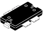
CASE 1486 - 03, STYLE 1
TO - 270 WB - 4
PLASTIC
MRF5S19060NR1
CASE 1484 - 04, STYLE 1
TO - 272 WB - 4
PLASTIC
MRF5S19060NBR1
Table 1. Maximum Ratings
Rating
Symbol
Value
Unit
Drain- Source Voltage
VDSS
- 0.5, +65
Vdc
Gate- Source Voltage
VGS
- 0.5, +15
Vdc
Total Device Dissipation @ TC = 25°C
Derate above 25°C
PD
218.8
1.25
W
W/°C
Storage Temperature Range
Tstg
- 65 to +175
°C
Operating Junction Temperature
TJ
200
°C
Symbol
Value (1,2)
Unit
Table 2. Thermal Characteristics
Characteristic
Thermal Resistance, Junction to Case
Case Temperature 75°C, 12 W CW
RθJC
0.80
°C/W
1. MTTF calculator available at http://www.freescale.com/rf. Select Software & Tools/Development Tools/Calculators to access MTTF
calculators by product.
2. Refer to AN1955, Thermal Measurement Methodology of RF Power Amplifiers. Go to http://www.freescale.com/rf.
Select Documentation/Application Notes - AN1955.
© Freescale Semiconductor, Inc., 2008. All rights reserved.
RF Device Data
Freescale Semiconductor
MRF5S19060NR1 MRF5S19060NBR1
1
�Table 3. ESD Protection Characteristics
Test Methodology
Class
Human Body Model (per JESD22 - A114)
1C (Minimum)
Machine Model (per EIA/JESD22 - A115)
C (Minimum)
Charge Device Model (per JESD22 - C101)
IV (Minimum)
Table 4. Moisture Sensitivity Level
Test Methodology
Per JESD 22 - A113, IPC/JEDEC J - STD - 020
Rating
Package Peak Temperature
Unit
3
260
°C
Table 5. Electrical Characteristics (TC = 25°C unless otherwise noted)
Symbol
Min
Typ
Max
Unit
Zero Gate Voltage Drain Leakage Current
(VDS = 65 Vdc, VGS = 0 Vdc)
IDSS
—
—
10
μAdc
Zero Gate Voltage Drain Leakage Current
(VDS = 28 Vdc, VGS = 0 Vdc)
IDSS
—
—
1
μAdc
Gate- Source Leakage Current
(VGS = 5 Vdc, VDS = 0 Vdc)
IGSS
—
—
1
μAdc
Gate Threshold Voltage
(VDS = 10 Vdc, ID = 225 μAdc)
VGS(th)
2.5
—
3.5
Vdc
Gate Quiescent Voltage
(VDS = 28 Vdc, ID = 750 mAdc)
VGS(Q)
—
3.8
—
Vdc
Drain- Source On - Voltage
(VGS = 5 Vdc, ID = 2.25 Adc)
VDS(on)
—
0.26
—
Vdc
Forward Transconductance
(VDS = 10 Vdc, ID = 2.25 Adc)
gfs
—
5
—
S
Crss
—
1.5
—
pF
Characteristic
Off Characteristics
On Characteristics
Dynamic Characteristics (1)
Reverse Transfer Capacitance
(VDS = 28 Vdc ± 30 mV(rms)ac @ 1 MHz, VGS = 0 Vdc)
Functional Tests (In Freescale Test Fixture, 50 ohm system) VDD = 28 Vdc, IDQ = 750 mA, Pout = 12 W Avg., f1 = 1987.5 MHz,
f2 = 1990 MHz, 2 - carrier N - CDMA, 1.2288 MHz Channel Bandwidth Carriers. ACPR measured in 30 kHz Channel Bandwidth @ ±885 kHz
Offset. IM3 measured in 1.2288 MHz Channel Bandwidth @ ±2.5 MHz Offset. PAR = 9.8 dB @ 0.01% Probability on CCDF.
Power Gain
Gps
12.5
14
16
dB
Drain Efficiency
ηD
21
23
—
%
Intermodulation Distortion
IM3
—
- 37
- 35
dBc
ACPR
—
- 51
- 48
dBc
IRL
—
- 12
-9
dB
Pulse Peak Power
(VDD = 28 Vdc, 1 - Tone CW Pulsed, IDQ = 750 mA, tON = 8 μs,
1% Duty Cycle)
Psat
—
110
—
W
Video Bandwidth
(VDD = 28 Vdc, Pout = 60 W PEP, IDQ = 750 mA, Tone Spacing =
1 MHz to VBW, Δ IM3