Freescale Semiconductor
Technical Data
Document Number: MRF6S9125
Rev. 2, 2/2006
Replaced by MRF6S9125NR1/NBR1. There are no form, fit or function changes with
this part replacement. N suffix added to part number to indicate transition to lead - free
terminations.
MRF6S9125MR1
MRF6S9125MBR1
RF Power Field Effect Transistors
N - Channel Enhancement - Mode Lateral MOSFETs
880 MHz, 27 W AVG., 28 V
SINGLE N - CDMA
LATERAL N - CHANNEL
RF POWER MOSFETs
N - CDMA Application
• Typical Single - Carrier N - CDMA Performance: VDD = 28 Volts, IDQ =
950 mA, Pout = 27 Watt Avg., Full Frequency Band (865 - 895 MHz), IS - 95
CDMA (Pilot, Sync, Paging, Traffic Codes 8 Through 13) Channel
Bandwidth = 1.2288 MHz. PAR = 9.8 dB @ 0.01% Probability on CCDF.
Power Gain — 20.2 dB
Drain Efficiency — 31%
ACPR @ 750 kHz Offset = - 47.1 dBc @ 30 kHz Bandwidth
GSM EDGE Application
• Typical GSM EDGE Performance: VDD = 28 Volts, IDQ = 700 mA,
Pout = 60 Watts Avg., Full Frequency Band (865 - 895 MHz or
921 - 960 MHz)
Power Gain — 20 dB
Drain Efficiency — 40% (Typ)
Spectral Regrowth @ 400 kHz Offset = - 63 dBc
Spectral Regrowth @ 600 kHz Offset = - 78 dBc
EVM — 1.5% rms
GSM Application
• Typical GSM Performance: VDD = 28 Volts, IDQ = 700 mA, Pout =
125 Watts, Full Frequency Band (921 - 960 MHz)
Power Gain — 19 dB
Drain Efficiency — 62%
• Capable of Handling 10:1 VSWR, @ 28 Vdc, @ P1dB Output Power,
@ f = 880 MHz
• Characterized with Series Equivalent Large - Signal Impedance Parameters
• Internally Matched for Ease of Use
• Qualified Up to a Maximum of 32 VDD Operation
• Integrated ESD Protection
• 200°C Capable Plastic Package
• In Tape and Reel. R1 Suffix = 500 Units per 44 mm, 13 inch Reel.
ARCHIVE INFORMATION
ARCHIVE INFORMATION
Designed for broadband commercial and industrial applications with
frequencies up to 1000 MHz. The high gain and broadband performance of
these devices make them ideal for large - signal, common - source amplifier
applications in 28 volt base station equipment.
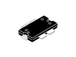
CASE 1486 - 03, STYLE 1
TO - 270 WB - 4
PLASTIC
MRF6S9125MR1
CASE 1484 - 03, STYLE 1
TO - 272 WB - 4
PLASTIC
MRF6S9125MBR1
Table 1. Maximum Ratings
Rating
Symbol
Value
Unit
Drain- Source Voltage
VDSS
- 0.5, +68
Vdc
Gate- Source Voltage
VGS
- 0.5, +12
Vdc
Total Device Dissipation @ TC = 25°C
Derate above 25°C
PD
398
2.3
W
W/°C
Storage Temperature Range
Tstg
- 65 to +150
°C
Operating Junction Temperature
TJ
200
°C
NOTE - CAUTION - MOS devices are susceptible to damage from electrostatic charge. Reasonable precautions in handling and
packaging MOS devices should be observed.
Freescale Semiconductor, Inc., 2006. All rights reserved.
RF Device Data
Freescale Semiconductor
MRF6S9125MR1 MRF6S9125MBR1
1
�Table 2. Thermal Characteristics
Characteristic
Value(1)
Symbol
Thermal Resistance, Junction to Case
Case Temperature 80°C, 125 W CW
Case Temperature 76°C, 27 W CW
RθJC
Unit
°C/W
0.44
0.45
Table 3. ESD Protection Characteristics
Test Methodology
Class
Human Body Model (per JESD22 - A114)
1B (Minimum)
Machine Model (per EIA/JESD22 - A115)
C (Minimum)
Charge Device Model (per JESD22 - C101)
IV (Minimum)
ARCHIVE INFORMATION
Test Methodology
Per JESD 22 - A113, IPC/JEDEC J - STD - 020
Rating
Package Peak Temperature
Unit
3
260
°C
Table 5. Electrical Characteristics (TC = 25°C unless otherwise noted)
Symbol
Min
Typ
Max
Unit
Zero Gate Voltage Drain Leakage Current
(VDS = 68 Vdc, VGS = 0 Vdc)
IDSS
—
—
10
µAdc
Zero Gate Voltage Drain Leakage Current
(VDS = 28 Vdc, VGS = 0 Vdc)
IDSS
—
—
1
µAdc
Gate- Source Leakage Current
(VGS = 5 Vdc, VDS = 0 Vdc)
IGSS
—
—
1
µAdc
Gate Threshold Voltage
(VDS = 10 Vdc, ID = 400 µAdc)
VGS(th)
1
2.1
3
Vdc
Gate Quiescent Voltage
(VDS = 28 Vdc, ID = 950 mAdc)
VGS(Q)
2
2.89
4
Vdc
Drain- Source On - Voltage
(VGS = 10 Vdc, ID = 2.74 Adc)
VDS(on)
0.05
0.23
0.3
Vdc
gfs
—
6
—
S
Output Capacitance
(VDS = 28 Vdc ± 30 mV(rms)ac @ 1 MHz, VGS = 0 Vdc)
Coss
—
60
—
pF
Reverse Transfer Capacitance
(VDS = 28 Vdc ± 30 mV(rms)ac @ 1 MHz, VGS = 0 Vdc)
Crss
—
2
—
pF
24
dB
Characteristic
Off Characteristics
On Characteristics
Forward Transconductance
(VDS = 10 Vdc, ID = 8 Adc)
Dynamic Characteristics (2)
Functional Tests (In Freescale Test Fixture, 50 ohm system) VDD = 28 Vdc, IDQ = 950 mA, Pout = 27 W, f = 880 MHz
Power Gain
Drain Efficiency
Adjacent Channel Power Ratio
Input Return Loss
Gps
19
20.2
ηD
29
31
—
%
ACPR
—
- 47.1
- 45
dBc
IRL
—
- 16
-9
dB
ARCHIVE INFORMATION
Table 4. Moisture Sensitivity Level
1. Refer to AN1955, Thermal Measurement Methodology of RF Power Amplifiers. Go to http://www.freescale.com/rf.
Select Documentation/Application Notes - AN1955.
2. Part is internally input matched.
(continued)
MRF6S9125MR1 MRF6S9125MBR1
2
RF Device Data
Freescale Semiconductor
�Table 5. Electrical Characteristics (TC = 25°C unless otherwise noted) (continued)
Characteristic
Symbol
Min
Typ
Max
Unit
Typical GSM EDGE Performances (In Freescale GSM EDGE Test Fixture, 50 οhm system) VDD = 28 Vdc, IDQ = 950 mA,
Pout = 60 W Avg., 921 MHz