Freescale Semiconductor
Technical Data
Document Number: MRF7S19120N
Rev. 3, 3/2011
RF Power Field Effect Transistor
N--Channel Enhancement--Mode Lateral MOSFET
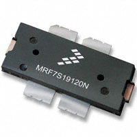
MRF7S19120NR1
Designed for CDMA base station applications with frequencies from 1930 to
1990 MHz. Can be used in Class AB and Class C for all typical cellular base
station modulation formats.
• Typical Single--Carrier W--CDMA Performance: VDD = 28 Volts, IDQ =
1200 mA, Pout = 36 Watts Avg., f = 1990 MHz, IQ Magnitude Clipping,
Channel Bandwidth = 3.84 MHz, Input Signal PAR = 7.5 dB @ 0.01%
Probability on CCDF.
Power Gain — 18 dB
Drain Efficiency — 32%
Device Output Signal PAR — 6.1 dB @ 0.01% Probability on CCDF
ACPR @ 5 MHz Offset — --38.5 dBc in 3.84 MHz Channel Bandwidth
• Capable of Handling 10:1 VSWR, @ 32 Vdc, 1960 MHz, 120 Watts CW
Output Power
• Pout @ 1 dB Compression Point ≃ 120 W CW
Features
• 100% PAR Tested for Guaranteed Output Power Capability
• Characterized with Series Equivalent Large--Signal Impedance Parameters
• Internally Matched for Ease of Use
• Integrated ESD Protection
• Greater Negative Gate--Source Voltage Range for Improved Class C
Operation
• Designed for Digital Predistortion Error Correction Systems
• 225°C Capable Plastic Package
• RoHS Compliant
• In Tape and Reel. R1 Suffix = 500 Units, 44 mm Tape Width, 13 inch Reel.
1930--1990 MHz, 36 W AVG., 28 V
SINGLE W--CDMA
LATERAL N--CHANNEL
RF POWER MOSFET
CASE 1730--02
TO--270 WBL--4
PLASTIC
Table 1. Maximum Ratings
Rating
Symbol
Value
Unit
Drain--Source Voltage
VDSS
--0.5, +65
Vdc
Gate--Source Voltage
VGS
--6.0, +10
Vdc
Operating Voltage
VDD
32, +0
Vdc
Storage Temperature Range
Tstg
-- 65 to +150
°C
Case Operating Temperature
TC
150
°C
Operating Junction Temperature (1,2)
TJ
225
°C
Symbol
Value (2,3)
Unit
Table 2. Thermal Characteristics
Characteristic
Thermal Resistance, Junction to Case
Case Temperature 81°C, 120 W CW
Case Temperature 80°C, 36 W CW
RθJC
0.43
0.51
°C/W
1. Continuous use at maximum temperature will affect MTTF.
2. MTTF calculator available at http://www.freescale.com/rf. Select Software & Tools/Development Tools/Calculators to access MTTF
calculators by product.
3. Refer to AN1955, Thermal Measurement Methodology of RF Power Amplifiers. Go to http://www.freescale.com/rf.
Select Documentation/Application Notes -- AN1955.
© Freescale Semiconductor, Inc., 2007, 2009, 2011. All rights reserved.
RF Device Data
Freescale Semiconductor
MRF7S19120NR1
1
�Table 3. ESD Protection Characteristics
Test Methodology
Class
Human Body Model (per JESD22--A114)
2 (Minimum)
Machine Model (per EIA/JESD22--A115)
A (Minimum)
Charge Device Model (per JESD22--C101)
III (Minimum)
Table 4. Moisture Sensitivity Level
Test Methodology
Per JESD22--A113, IPC/JEDEC J--STD--020
Rating
Package Peak Temperature
Unit
3
260
°C
Table 5. Electrical Characteristics (TA = 25°C unless otherwise noted)
Symbol
Min
Typ
Max
Unit
Zero Gate Voltage Drain Leakage Current
(VDS = 65 Vdc, VGS = 0 Vdc)
IDSS
—
—
10
μAdc
Zero Gate Voltage Drain Leakage Current
(VDS = 28 Vdc, VGS = 0 Vdc)
IDSS
—
—
1
μAdc
Gate--Source Leakage Current
(VGS = 5 Vdc, VDS = 0 Vdc)
IGSS
—
—
1
μAdc
Gate Threshold Voltage
(VDS = 10 Vdc, ID = 270 μAdc)
VGS(th)
1.2
2
2.7
Vdc
Gate Quiescent Voltage
(VDD = 28 Vdc, ID = 1200 mAdc, Measured in Functional Test)
VGS(Q)
2
2.7
3.5
Vdc
Drain--Source On--Voltage
(VGS = 10 Vdc, ID = 2.7 Adc)
VDS(on)
0.15
0.275
0.35
Vdc
Reverse Transfer Capacitance
(VDS = 28 Vdc ± 30 mV(rms)ac @ 1 MHz, VGS = 0 Vdc)
Crss
—
1.65
—
pF
Output Capacitance
(VDS = 28 Vdc ± 30 mV(rms)ac @ 1 MHz, VGS = 0 Vdc)
Coss
—
600
—
pF
Input Capacitance
(VDS = 28 Vdc, VGS = 0 Vdc ± 30 mV(rms)ac @ 1 MHz)
Ciss
—
1.03
—
pF
Characteristic
Off Characteristics
On Characteristics
Dynamic Characteristics (1)
Functional Tests (In Freescale Test Fixture, 50 ohm system) VDD = 28 Vdc, IDQ = 1200 mA, Pout = 36 W Avg., f = 1990 MHz, Single--Carrier
W--CDMA, IQ Magnitude Clipping, Input Signal PAR = 7.5 dB @ 0.01% Probability on CCDF. ACPR measured in 3.84 MHz Channel
Bandwidth @ ±5 MHz Offset.
Power Gain
Gps
16.5
18
19.5
dB
Drain Efficiency
ηD
30
32
36
%
Output Peak--to--Average Ratio @ 0.01% Probability on CCDF
Adjacent Channel Power Ratio
Input Return Loss
PAR
5.7
6.1
—
dB
ACPR
—
--38.5
--35.5
dBc
IRL
—
--10
--7
dB
1. Part internally matched both on input and output.
(continued)
MRF7S19120NR1
2
RF Device Data
Freescale Semiconductor
�Table 5. Electrical Characteristics (TA = 25°C unless otherwise noted) (continued)
Characteristic
Symbol
Min
Typ
Max
Unit
Typical Performances (In Freescale Test Fixture, 50 ohm system) VDD = 28 Vdc, IDQ = 1200 mA, 1930--1990 MHz Bandwidth
Video Bandwidth @ 120 W PEP Pout where IM3 = --30 dBc
(Tone Spacing from 100 kHz to VBW)
∆IMD3 = IMD3 @ VBW frequency -- IMD3 @ 100 kHz Software and Tools.
MRF7S19120NR1
RF Device Data
Freescale Semiconductor
13
�How to Reach Us:
Home Page:
www.freescale.com
Web Support:
http://www.freescale.com/support
USA/Europe or Locations Not Listed:
Freescale Semiconductor, Inc.
Technical Information Center, EL516
2100 East Elliot Road
Tempe, Arizona 85284
1--800--521--6274 or +1--480--768--2130
www.freescale.com/support
Europe, Middle East, and Africa:
Freescale Halbleiter Deutschland GmbH
Technical Information Center
Schatzbogen 7
81829 Muenchen, Germany
+44 1296 380 456 (English)
+46 8 52200080 (English)
+49 89 92103 559 (German)
+33 1 69 35 48 48 (French)
www.freescale.com/support
Japan:
Freescale Semiconductor Japan Ltd.
Headquarters
ARCO Tower 15F
1--8--1, Shimo--Meguro, Meguro--ku,
Tokyo 153--0064
Japan
0120 191014 or +81 3 5437 9125
support.japan@freescale.com
Asia/Pacific:
Freescale Semiconductor China Ltd.
Exchange Building 23F
No. 118 Jianguo Road
Chaoyang District
Beijing 100022
China
+86 10 5879 8000
support.asia@freescale.com
For Literature Requests Only:
Freescale Semiconductor Literature Distribution Center
1--800--441--2447 or +1--303--675--2140
Fax: +1--303--675--2150
LDCForFreescaleSemiconductor@hibbertgroup.com
Information in this document is provided solely to enable system and software
implementers to use Freescale Semiconductor products. There are no express or
implied copyright licenses granted hereunder to design or fabricate any integrated
circuits or integrated circuits based on the information in this document.
Freescale Semiconductor reserves the right to make changes without further notice to
any products herein. Freescale Semiconductor makes no warranty, representation or
guarantee regarding the suitability of its products for any particular purpose, nor does
Freescale Semiconductor assume any liability arising out of the application or use of
any product or circuit, and specifically disclaims any and all liability, including without
limitation consequential or incidental damages. “Typical” parameters that may be
provided in Freescale Semiconductor data sheets and/or specifications can and do
vary in different applications and actual performance may vary over time. All operating
parameters, including “Typicals”, must be validated for each customer application by
customer’s technical experts. Freescale Semiconductor does not convey any license
under its patent rights nor the rights of others. Freescale Semiconductor products are
not designed, intended, or authorized for use as components in systems intended for
surgical implant into the body, or other applications intended to support or sustain life,
or for any other application in which the failure of the Freescale Semiconductor product
could create a situation where personal injury or death may occur. Should Buyer
purchase or use Freescale Semiconductor products for any such unintended or
unauthorized application, Buyer shall indemnify and hold Freescale Semiconductor
and its officers, employees, subsidiaries, affiliates, and distributors harmless against all
claims, costs, damages, and expenses, and reasonable attorney fees arising out of,
directly or indirectly, any claim of personal injury or death associated with such
unintended or unauthorized use, even if such claim alleges that Freescale
Semiconductor was negligent regarding the design or manufacture of the part.
Freescalet and the Freescale logo are trademarks of Freescale Semiconductor, Inc.
All other product or service names are the property of their respective owners.
© Freescale Semiconductor, Inc. 2007, 2009, 2011. All rights reserved.
MRF7S19120NR1
Document Number: MRF7S19120N
Rev. 3, 3/2011
14
RF Device Data
Freescale Semiconductor
�