Freescale Semiconductor
Technical Data
Document Number: MRFE6S9060N
Rev. 1, 10/2007
RF Power Field Effect Transistor
N - Channel Enhancement - Mode Lateral MOSFET
MRFE6S9060NR1
Designed for broadband commercial and industrial applications with
frequencies up to 1000 MHz. The high gain and broadband performance of
this device makes it ideal for large - signal, common - source amplifier
applications in 28 volt base station equipment.
• Typical Single - Carrier N - CDMA Performance @ 880 MHz, VDD = 28 Volts,
IDQ = 450 mA, Pout = 14 Watts Avg., IS - 95 CDMA (Pilot, Sync, Paging,
Traffic Codes 8 Through 13) Channel Bandwidth = 1.2288 MHz. PAR =
9.8 dB @ 0.01% Probability on CCDF.
Power Gain — 21.1 dB
Drain Efficiency — 33%
ACPR @ 750 kHz Offset — - 45.7 dBc in 30 kHz Channel Bandwidth
• Capable of Handling 10:1 VSWR, @ 32 Vdc, 880 MHz, 3 dB Overdrive,
Designed for Enhanced Ruggedness
GSM EDGE Application
• Typical GSM EDGE Performance: VDD = 28 Volts, IDQ = 500 mA,
Pout = 21 Watts Avg., Full Frequency Band (920 - 960 MHz)
Power Gain — 20 dB
Drain Efficiency — 46%
Spectral Regrowth @ 400 kHz Offset = - 62 dBc
Spectral Regrowth @ 600 kHz Offset = - 78 dBc
EVM — 1.5% rms
GSM Application
• Typical GSM Performance: VDD = 28 Volts, IDQ = 500 mA, Pout = 60 Watts,
Full Frequency Band (920 - 960 MHz)
Power Gain — 20 dB
Drain Efficiency — 63%
Features
• Characterized with Series Equivalent Large - Signal Impedance Parameters
• Integrated ESD Protection
• 225°C Capable Plastic Package
• RoHS Compliant
• In Tape and Reel. R1 Suffix = 500 Units per 24 mm, 13 inch Reel.
880 MHz, 14 W AVG., 28 V
SINGLE N - CDMA
LATERAL N - CHANNEL
BROADBAND
RF POWER MOSFET
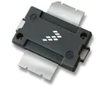
CASE 1265- 09, STYLE 1
TO - 270 - 2
PLASTIC
Table 1. Maximum Ratings
Rating
Symbol
Value
Unit
Drain - Source Voltage
VDSS
- 0.5, +66
Vdc
Gate - Source Voltage
VGS
- 0.5, + 12
Vdc
Maximum Operation Voltage
VDD
32, +0
Vdc
Storage Temperature Range
Tstg
- 65 to +150
°C
Case Operating Temperature
TC
150
°C
Operating Junction Temperature (1,2)
TJ
225
°C
Symbol
Value (2,3)
Unit
Table 2. Thermal Characteristics
Characteristic
Thermal Resistance, Junction to Case
Case Temperature 80°C, 60 W CW
Case Temperature 78°C, 14 W CW
RθJC
0.77
0.88
°C/W
1. Continuous use at maximum temperature will affect MTTF.
2. MTTF calculator available at http://www.freescale.com/rf. Select Tools (Software & Tools)/Calculators to access MTTF calculators
by product.
3. Refer to AN1955, Thermal Measurement Methodology of RF Power Amplifiers. Go to http://www.freescale.com/rf.
Select Documentation/Application Notes - AN1955.
© Freescale Semiconductor, Inc., 2007. All rights reserved.
RF Device Data
Freescale Semiconductor
MRFE6S9060NR1
1
�Table 3. ESD Protection Characteristics
Test Methodology
Class
Human Body Model (per JESD22 - A114)
2 (Minimum)
Machine Model (per EIA/JESD22 - A115)
B (Minimum)
Charge Device Model (per JESD22 - C101)
III (Minimum)
Table 4. Moisture Sensitivity Level
Test Methodology
Per JESD 22 - A113, IPC/JEDEC J - STD - 020
Rating
Package Peak Temperature
Unit
3
260
°C
Table 5. Electrical Characteristics (TC = 25°C unless otherwise noted)
Characteristic
Symbol
Min
Typ
Max
Unit
Zero Gate Voltage Drain Leakage Current
(VDS = 66 Vdc, VGS = 0 Vdc)
IDSS
—
—
10
μAdc
Zero Gate Voltage Drain Leakage Current
(VDS = 28 Vdc, VGS = 0 Vdc)
IDSS
—
—
1
μAdc
Gate - Source Leakage Current
(VGS = 5 Vdc, VDS = 0 Vdc)
IGSS
—
—
10
μAdc
Gate Threshold Voltage
(VDS = 10 Vdc, ID = 200 μA)
VGS(th)
1
2.2
3
Vdc
Gate Quiescent Voltage
(VDD = 28 Vdc, ID = 450 mAdc, Measured in Functional Test)
VGS(Q)
2
3
4
Vdc
Drain - Source On - Voltage
(VGS = 10 Vdc, ID = 1.5 Adc)
VDS(on)
0.05
0.27
0.4
Vdc
Reverse Transfer Capacitance
(VDS = 28 Vdc ± 30 mV(rms)ac @ 1 MHz, VGS = 0 Vdc)
Crss
—
1.1
—
pF
Output Capacitance
(VDS = 28 Vdc ± 30 mV(rms)ac @ 1 MHz, VGS = 0 Vdc)
Coss
—
33
—
pF
Input Capacitance
(VDS = 28 Vdc, VGS = 0 Vdc ± 30 mV(rms)ac @ 1 MHz)
Ciss
—
109
—
pF
Off Characteristics
On Characteristics
Dynamic Characteristics
Functional Tests (In Freescale Test Fixture, 50 ohm system) VDD = 28 Vdc, IDQ = 450 mA, Pout = 14 W Avg., f = 880 MHz, Single - Carrier
N - CDMA, 1.2288 MHz Channel Bandwidth Carrier. ACPR measured in 30 kHz Channel Bandwidth @ ±750 kHz Offset. PAR = 9.8 dB @
0.01% Probability on CCDF
Power Gain
Gps
20
21.1
23
dB
Drain Efficiency
ηD
30.5
33
—
%
ACPR
—
- 45.7
- 44
dBc
IRL
—
- 18
-9
Adjacent Channel Power Ratio
Input Return Loss
dB
(continued)
MRFE6S9060NR1
2
RF Device Data
Freescale Semiconductor
�Table 5. Electrical Characteristics (TC = 25°C unless otherwise noted) (continued)
Characteristic
Symbol
Min
Typ
Max
Unit
Typical GSM EDGE Performances (In Freescale GSM EDGE Test Fixture Optimized for 920 - 960 MHz, 50 ohm system) VDD = 28 Vdc,
IDQ = 500 mA, Pout = 21 W Avg., f = 920 - 960 MHz, GSM EDGE Signal
Power Gain
Gps
—
20
—
dB
Drain Efficiency
ηD
—
46
—
%
Error Vector Magnitude
EVM
—
1.5
—
%
Spectral Regrowth at 400 kHz Offset
SR1
—
- 62
—
dBc
Spectral Regrowth at 600 kHz Offset
SR2
—
- 78
—
dBc
Typical CW Performances (In Freescale GSM Test Fixture Optimized for 920 - 960 MHz, 50 ohm system) VDD = 28 Vdc, IDQ = 500 mA,
Pout = 60 W, f = 920 - 960 MHz
Power Gain
Gps
—
20
—
dB
Drain Efficiency
ηD
—
63
—
%
IRL
—
- 12
—
dB
P1dB
—
67
—
W
Input Return Loss
Pout @ 1 dB Compression Point
(f = 940 MHz)
Typical Performances (In Freescale Test Fixture, 50 ohm system) VDD = 28 Vdc, IDQ = 450 mA, 865 - 900 MHz Bandwidth
Video Bandwidth @ 60 W PEP Pout where IM3 = - 30 dBc
VBW
(Tone Spacing from 100 kHz to VBW)
—
3
—
ΔIMD3 = IMD3 @ VBW frequency - IMD3 @ 100 kHz