Document Number: MRFG35002N6A
Rev. 2, 6/2009
Gallium Arsenide PHEMT
RF Power Field Effect Transistor
MRFG35002N6AT1
LIFETIME BUY
Designed for WLL/MMDS/BWA or UMTS driver applications. Characterized
from 500 to 5000 MHz. Device is unmatched and is suitable for use in Class AB
Customer Premise Equipment (CPE) applications.
• Typical Single--Carrier W--CDMA Performance: VDD = 6 Volts, IDQ =
65 mA, Pout = 158 mWatts Avg., 3550 MHz, Channel Bandwidth =
3.84 MHz, PAR = 8.5 dB @ 0.01% Probability on CCDF.
Power Gain — 10 dB
Drain Efficiency — 26.5%
ACPR @ 5 MHz Offset — --42 dBc in 3.84 MHz Channel Bandwidth
• 1.5 Watts P1dB @ 3550 MHz, CW
Features
• Excellent Phase Linearity and Group Delay Characteristics
• High Gain, High Efficiency and High Linearity
• RoHS Compliant
• In Tape and Reel. T1 Suffix = 1000 Units per 12 mm, 7 inch Reel.
3.5 GHz, 1.5 W, 6 V
POWER FET
GaAs PHEMT
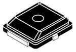
CASE 466--03, STYLE 1
PLD--1.5
PLASTIC
Table 1. Maximum Ratings
Rating
Symbol
Value
Unit
Drain--Source Voltage
VDSS
8
Vdc
Gate--Source Voltage
VGS
--5
Vdc
RF Input Power
Pin
22
dBm
Tstg
--65 to +150
°C
Tch
175
°C
Symbol
Value (2)
Unit
RθJC
13.7
°C/W
Storage Temperature Range
Channel Temperature
(1)
Table 2. Thermal Characteristics
Characteristic
Thermal Resistance, Junction to Case
1. For reliable operation, the operating channel temperature should not exceed 150°C.
2. Refer to AN1955, Thermal Measurement Methodology of RF Power Amplifiers. Go to http://www.freescale.com/rf.
Select Documentation/Application Notes -- AN1955.
© Freescale Semiconductor, Inc., 2007--2009. All rights reserved.
RF Device Data
Freescale Semiconductor
LAST ORDER 1 JUL 11 LAST SHIP 30 JUN 12
Freescale Semiconductor
Technical Data
MRFG35002N6AT1
1
�Table 3. ESD Protection Characteristics
Class
Human Body Model (per JESD22--A114)
1C (Minimum)
Machine Model (per EIA/JESD22--A115)
A (Minimum)
Charge Device Model (per JESD22--C101)
IV (Minimum)
Table 4. Moisture Sensitivity Level
Test Methodology
Rating
Package Peak Temperature
Unit
3
260
°C
Per JESD22--A113, IPC/JEDEC J--STD--020
Table 5. Electrical Characteristics (TA = 25°C unless otherwise noted)
Symbol
Min
Typ
Max
Unit
Saturated Drain Current
(VDS = 3.5 Vdc, VGS = 0 Vdc)
IDSS
—
1.7
—
Adc
Off State Leakage Current
(VGS = --0.4 Vdc, VDS = 0 Vdc)
IGSS
—
< 1.0
100
μAdc
Off State Drain Current
(VDS = 6 Vdc, VGS = --2.5 Vdc)
IDSO
—
—
600
μAdc
Off State Current
(VDS = 28.5 Vdc, VGS = --2.5 Vdc)
IDSX
—
< 1.0
9
mAdc
Gate--Source Cut--off Voltage
(VDS = 3.5 Vdc, IDS = 8.7 mA)
VGS(th)
--1.2
--0.95
--0.7
Vdc
Quiescent Gate Voltage
(VDS = 6 Vdc, ID = 65 mA)
VGS(Q)
--1.1
--0.85
--0.6
Vdc
LIFETIME BUY
Characteristic
Functional Tests (In Freescale Test Fixture, 50 ohm system) VDD = 6 Vdc, IDQ = 65 mA, Pout = 158 mW Avg., f = 3550 MHz, Single--Carrier
W--CDMA, 3.84 MHz Channel Bandwidth Carrier. ACPR measured in 3.84 MHz Channel Bandwidth @ ±5 MHz Offset.
PAR = 8.5 dB @ 0.01% Probability on CCDF.
Power Gain
Gps
8.5
10
—
dB
Drain Efficiency
ηD
23
26.5
—
%
ACPR
—
--42
--38
dBc
—
W
Adjacent Channel Power Ratio
Typical RF Performance (In Freescale Test Fixture, 50 ohm system) VDD = 6 Vdc, IDQ = 65 mA, f = 3550 MHz
Pout @ 1 dB Compression Point, CW
P1dB
—
1.5
LAST ORDER 1 JUL 11 LAST SHIP 30 JUN 12
Test Methodology
MRFG35002N6AT1
2
RF Device Data
Freescale Semiconductor
�C8
C18
VBIAS
VSUPPLY
C12
C11
C10
C7
C9
C17
C16
C15
C14
C19
R1
C6
C20
C5
C22
RF
INPUT
Z6
Z1
Z2
Z3
Z5
Z4
C21
Z11
Z7
Z8
Z9
Z10
Z12
Z13
C1
C24
C3
LIFETIME BUY
Z14
RF
OUTPUT
Z1, Z14
Z2
Z3
Z4
Z5
Z6, Z11
Z7
C4
C23
0.044″ x 0.125″ Microstrip
0.044″ x 0.481″ Microstrip
0.044″ x 0.076″ Microstrip
0.468″ x 0.025″ Microstrip
0.468″ x 0.341″ Microstrip
0.015″ x 0.549″ Microstrip
0.031″ x 0.259″ Microstrip
Z8
Z9
Z10
Z12
Z13
PCB
0.420″ x 0.150″ Microstrip
0.150″ x 0.068″ Microstrip
0.290″ x 0.183″ Microstrip
0.044″ x 0.291″ Microstrip
0.044″ x 0.808″ Microstrip
Rogers 4350, 0.020″, εr = 3.5
Figure 1. MRFG35002N6A Test Circuit Schematic
Table 6. MRFG35002N6A Test Circuit Component Designations and Values
Part
Description
C1, C24
13 pF Chip Capacitors
C2
Not used
C3
C4
Part Number
Manufacturer
ATC100A130JT500XT
ATC
1.2 pF Chip Capacitor
08051J1R2BBS
AVX
0.7 pF Chip Capacitor
08051J0R7BBS
AVX
C5, C6, C21, C22
5.6 pF Chip Capacitors
08051J5R6BBS
AVX
C7, C20
10 pF Chip Capacitors
ATC100A100JT500XT
ATC
C8, C19
100 pF Chip Capacitors
ATC100A101JT500XT
ATC
C9, C18
100 pF Chip Capacitors
ATC100B101JT500XT
ATC
C10, C17
1000 pF Chip Capacitors
ATC100B102JT50XT
ATC
C11, C16
0.01 μF Chip Capacitors
ATC200B103KT50XT
ATC
C12, C15
39K pF Chip Capacitors
ATC200B393KT50XT
ATC
C13, C14
10 μF Chip Capacitors
GRM55DR61H106KA88B
Murata
C23
0.2 pF Chip Capacitor
08051J0R2BBS
AVX
R1
100 Ω, 1/4 W Chip Resistor
CRCW12061000FKEA
Vishay
LAST ORDER 1 JUL 11 LAST SHIP 30 JUN 12
C13
MRFG35002N6AT1
RF Device Data
Freescale Semiconductor
3
�C12
C11
C10
C17
C18
C9
C16
C15
C14
C8
C7
R1
C5
C6
C19
C20
LIFETIME BUY
C22
C21
C2
C1
C23
C3
C24
C4
MRFG35002N6A Rev. 3
Figure 2. MRFG35002N6A Test Circuit Component Layout
LAST ORDER 1 JUL 11 LAST SHIP 30 JUN 12
C13
MRFG35002N6AT1
4
RF Device Data
Freescale Semiconductor
�TYPICAL CHARACTERISTICS
60
VDD = 6 Vdc, IDQ = 65 mA, f = 3550 MHz
Single--Carrier W--CDMA, 3.84 MHz Channel
Bandwidth, PAR = 8.5 dB @ 0.01% Probability (CCDF)
50
40
10
Gps
8
30
20
6
ηD
4
10
2
ηD, DRAIN EFFICIENCY (%)
Gps, POWER GAIN (dB)
12
0
14
16
18
20
22
24
26
28
Figure 3. Single--Channel W--CDMA Power Gain
and Drain Efficiency versus Output Power
0
0
VDD = 6 Vdc, IDQ = 65 mA, f = 3550 MHz
Single--Carrier W--CDMA, 3.84 MHz Channel
Bandwidth, PAR = 8.5 dB @ 0.01% Probability (CCDF)
--10
--5
--10
--20
IRL
--30
--15
--40
--20
IRL, INPUT RETURN LOSS (dB)
ACPR, ADJACENT CHANNEL POWER RATIO (dBc)
ACPR
--50
14
16
18
20
22
24
26
28
--25
Pout, OUTPUT POWER (dBm)
Figure 4. Single--Channel W--CDMA Adjacent
Channel Power Ratio and IRL versus Output Power
14
Gps, POWER GAIN (dB)
12
36
VDD = 6 Vdc, IDQ = 65 mA, Pout = 158 mW
Single--Carrier W--CDMA, 3.84 MHz Channel
Bandwidth, PAR = 8.5 dB @ 0.01% Probability (CCDF)
10
34
32
Gps
8
30
6
28
ηD
4
26
2
3450
3500
3550
3600
24
3650
f, FREQUENCY (MHz)
Figure 5. Single--Channel W--CDMA Power Gain
and Drain Efficiency versus Frequency
ηD, DRAIN EFFICIENCY (%)
LIFETIME BUY
Pout, OUTPUT POWER (dBm)
LAST ORDER 1 JUL 11 LAST SHIP 30 JUN 12
14
NOTE: Data is generated from the test circuit shown.
MRFG35002N6AT1
RF Device Data
Freescale Semiconductor
5
�0
--10
--20
--5
--10
IRL
--30
--15
--40
--20
ACPR
--50
3400
3450
3500
3550
3600
3650
--25
3700
Figure 6. Single--Channel W--CDMA Adjacent
Channel Power Ratio and IRL versus Frequency
--5
60
VDD = 6 Vdc, IDQ = 65 mA, f = 3550 MHz
Single--Carrier OFDM 802.16d, 64 QAM 3/4
7 MHz Channel Bandwidth, Input Signal PAR = 9.5 dB
@ 0.01% Probability on CCDF
--10
--15
50
40
--20
30
--25
20
ηD
--30
10
EVM
--35
14
16
18
0
20
22
24
26
28
Pout, OUTPUT POWER (dBm)
Figure 7. Single--Channel OFDM Error Vector Magnitude
and Drain Efficiency versus Output Power
NOTE: Data is generated from the test circuit shown.
ηD, DRAIN EFFICIENCY (%)
EVM, ERROR VECTOR MAGNITUDE (dB)
LIFETIME BUY
f, FREQUENCY (MHz)
LAST ORDER 1 JUL 11 LAST SHIP 30 JUN 12
0
VDD = 6 Vdc, IDQ = 65 mA, Pout = 158 mW
Single--Carrier W--CDMA, 3.84 MHz Channel
Bandwidth, PAR = 8.5 dB @ 0.01% Probability (CCDF)
IRL, INPUT RETURN LOSS (dB)
ACPR, ADJACENT CHANNEL POWER RATIO (dBc)
TYPICAL CHARACTERISTICS
MRFG35002N6AT1
6
RF Device Data
Freescale Semiconductor
�S11
S21
S12
f
MHz
|S11|
∠φ
|S21|
∠φ
|S12|
500
0.910
--175.1
5.223
82.8
550
0.911
--176.9
4.775
80.9
600
0.911
--178.5
4.396
650
0.911
--179.9
700
0.910
178.8
750
0.910
800
0.910
850
S22
∠φ
|S22|
∠φ
0.036
0.0
0.703
--176.6
0.036
--1.2
0.702
--177.9
79.1
0.036
--2.3
0.701
--179.1
4.078
77.4
0.037
--3.3
0.699
179.6
3.808
75.7
0.037
--4.4
0.698
178.5
177.7
3.574
74.0
0.037
--5.3
0.697
177.3
176.6
3.371
72.5
0.037
--6.2
0.696
176.1
0.910
175.7
3.191
70.9
0.037
--7.1
0.695
175.0
900
0.910
174.9
3.029
69.4
0.037
--7.8
0.694
173.8
950
0.910
174.2
2.883
67.9
0.037
--8.7
0.693
172.7
1000
0.909
173.4
2.748
66.3
0.037
--9.5
0.692
171.5
1050
0.910
172.7
2.632
65.0
0.037
--10.3
0.692
170.3
1100
0.910
172.1
2.520
63.5
0.038
--11.0
0.691
169.1
1150
0.909
171.4
2.421
62.0
0.038
--11.9
0.690
168.0
1200
0.910
170.8
2.329
60.6
0.038
--12.6
0.691
167.0
1250
0.909
170.1
2.246
59.2
0.038
--13.3
0.690
165.9
1300
0.908
169.5
2.168
57.8
0.038
--14.1
0.689
164.9
1350
0.907
168.8
2.097
56.4
0.038
--14.9
0.689
164.0
1400
0.907
168.1
2.030
54.9
0.038
--15.4
0.690
163.0
1450
0.907
167.2
1.968
53.5
0.038
--16.4
0.690
162.1
1500
0.906
166.3
1.911
52.0
0.038
--17.1
0.690
161.3
1550
0.904
163.0
1.874
50.4
0.039
--18.0
0.687
162.6
1600
0.903
162.2
1.823
49.0
0.039
--18.8
0.686
161.8
1650
0.903
161.3
1.775
47.6
0.039
--19.6
0.685
161.0
1700
0.903
160.5
1.729
46.2
0.039
--20.5
0.686
160.1
1750
0.902
159.8
1.686
44.7
0.039
--21.0
0.686
159.3
1800
0.902
158.9
1.645
43.3
0.039
--21.8
0.685
158.4
1850
0.901
158.1
1.607
41.9
0.039
--22.5
0.685
157.5
1900
0.901
157.4
1.570
40.5
0.039
--23.3
0.686
156.7
1950
0.902
156.6
1.535
39.1
0.039
--24.1
0.686
155.8
2000
0.901
155.9
1.502
37.7
0.039
--24.9
0.686
155.0
2050
0.901
155.1
1.470
36.3
0.039
--25.6
0.686
154.1
2100
0.901
154.3
1.441
34.9
0.040
--26.5
0.685
153.4
2150
0.906
153.3
1.415
33.5
0.040
--27.2
0.689
152.3
2200
0.900
152.8
1.388
32.0
0.040
--28.1
0.686
151.8
2250
0.900
151.9
1.364
30.6
0.040
--28.7
0.685
150.9
2300
0.899
151.0
1.342
29.2
0.040
--29.6
0.684
150.0
2350
0.898
150.2
1.321
27.7
0.040
--30.3
0.683
149.2
2400
0.899
149.3
1.302
26.2
0.040
--31.4
0.683
148.4
2450
0.897
148.4
1.284
24.8
0.041
--32.1
0.681
147.4
2500
0.896
147.4
1.268
23.3
0.041
--33.2
0.679
146.6
2550
0.896
146.5
1.254
21.8
0.041
--34.1
0.678
145.7
2600
0.893
145.4
1.240
20.2
0.041
--34.8
0.675
144.8
2650
0.894
144.5
1.227
18.7
0.042
--35.6
0.674
143.9
2700
0.891
143.4
1.216
17.2
0.042
--36.7
0.672
142.9
2750
0.891
142.4
1.206
15.6
0.042
--37.4
0.669
142.0
LAST ORDER 1 JUL 11 LAST SHIP 30 JUN 12
LIFETIME BUY
Table 7. Common Source S--Parameters (VDD = 6 Vdc, IDQ = 65 mA, TA = 25°C, 50 Ohm System)
(continued)
MRFG35002N6AT1
RF Device Data
Freescale Semiconductor
7
�S11
S21
S12
S22
f
MHz
|S11|
∠φ
|S21|
∠φ
|S12|
∠φ
|S22|
∠φ
2800
0.890
141.2
1.197
14.0
0.043
--38.6
0.667
141.1
2850
0.887
140.1
1.189
12.4
0.043
--39.5
0.663
140.2
2900
0.888
138.9
1.182
10.8
0.043
--40.4
0.661
139.2
2950
0.886
137.6
1.175
9.1
0.044
--41.4
0.658
138.2
3000
0.886
136.4
1.170
7.5
0.044
--42.4
0.656
137.2
3050
0.885
135.1
1.163
5.8
0.045
--43.5
0.652
136.3
3100
0.882
133.8
1.159
4.1
0.045
--44.5
0.649
135.2
3150
0.881
132.5
1.155
2.4
0.046
--45.5
0.645
134.2
3200
0.879
131.1
1.151
0.7
0.046
--46.8
0.642
133.1
3250
0.877
129.8
1.148
--1.0
0.047
--47.7
0.638
132.0
3300
0.876
128.4
1.145
--2.7
0.047
--48.9
0.634
130.9
3350
0.875
127.0
1.143
--4.5
0.048
--50.0
0.630
129.8
3400
0.874
125.6
1.141
--6.3
0.048
--51.3
0.627
128.7
3450
0.873
124.1
1.139
--8.0
0.049
--52.4
0.624
127.5
3500
0.870
122.6
1.137
--9.8
0.049
--53.8
0.620
126.4
3550
0.869
121.1
1.134
--11.6
0.050
--55.0
0.616
125.2
3600
0.867
119.7
1.133
--13.4
0.050
--56.2
0.612
124.0
3650
0.867
118.1
1.131
--15.2
0.051
--57.3
0.609
122.8
3700
0.865
116.6
1.130
--17.0
0.051
--58.4
0.605
121.5
3750
0.863
115.0
1.128
--18.8
0.052
--59.5
0.602
120.2
3800
0.861
113.5
1.127
--20.7
0.052
--60.9
0.598
118.9
3850
0.860
111.9
1.126
--22.5
0.053
--62.1
0.595
117.6
3900
0.858
110.3
1.125
--24.4
0.053
--63.4
0.591
116.2
3950
0.856
108.6
1.124
--26.3
0.054
--64.5
0.588
114.9
4000
0.854
107.0
1.122
--28.3
0.054
--65.7
0.585
113.4
4050
0.853
105.3
1.122
--30.2
0.055
--67.0
0.582
112.0
4100
0.851
103.5
1.122
--32.1
0.055
--68.1
0.579
110.5
4150
0.849
101.7
1.121
--34.2
0.056
--69.5
0.575
109.0
4200
0.847
99.8
1.120
--36.2
0.057
--70.9
0.572
107.4
4250
0.845
97.9
1.119
--38.3
0.057
--72.4
0.569
105.9
4300
0.842
96.0
1.119
--40.4
0.057
--73.8
0.566
104.2
4350
0.841
94.1
1.119
--42.6
0.058
--75.2
0.563
102.4
4400
0.838
92.0
1.118
--44.7
0.058
--76.6
0.559
100.7
4450
0.836
89.9
1.118
--47.0
0.059
--78.4
0.557
98.8
4500
0.836
87.7
1.118
--49.3
0.060
--80.0
0.553
96.8
4550
0.832
85.3
1.116
--51.7
0.060
--81.7
0.550
94.8
4600
0.828
83.3
1.114
--54.0
0.061
--83.3
0.547
92.7
4650
0.830
80.6
1.114
--56.4
0.061
--85.0
0.542
90.5
4700
0.826
78.3
1.114
--58.8
0.062
--86.6
0.539
88.3
4750
0.830
75.9
1.111
--61.3
0.062
--88.6
0.535
85.9
4800
0.827
72.9
1.109
--64.0
0.063
--90.6
0.532
83.6
4850
0.827
70.4
1.107
--66.6
0.063
--92.6
0.529
81.0
4900
0.828
67.5
1.104
--69.2
0.064
--94.4
0.525
78.4
4950
0.824
64.8
1.099
--71.8
0.064
--96.4
0.522
75.8
5000
0.824
61.8
1.095
--74.6
0.064
--98.6
0.518
72.9
LAST ORDER 1 JUL 11 LAST SHIP 30 JUN 12
LIFETIME BUY
Table 7. Common Source S--Parameters (VDD = 6 Vdc, IDQ = 65 mA, TA = 25°C, 50 Ohm System) (continued)
MRFG35002N6AT1
8
RF Device Data
Freescale Semiconductor
�PACKAGE DIMENSIONS
0.146
3.71
A
F
0.095
2.41
3
B
D
1
2
R
0.115
2.92
0.115
2.92
L
0.020
0.51
4
0.35 (0.89) X 45_ 5 _
N
K
Q
C
4
ZONE W
2
1
3
S
G
Y
Y
E
NOTES:
1. INTERPRET DIMENSIONS AND TOLERANCES
PER ASME Y14.5M, 1984.
2. CONTROLLING DIMENSION: INCH
3. RESIN BLEED/FLASH ALLOWABLE IN ZONE V, W,
AND X.
STYLE 1:
PIN 1.
2.
3.
4.
DRAIN
GATE
SOURCE
SOURCE
ZONE X
VIEW Y--Y
mm
SOLDER FOOTPRINT
P
U
H
ZONE V
inches
10_DRAFT
CASE 466--03
ISSUE D
PLD--1.5
PLASTIC
DIM
A
B
C
D
E
F
G
H
J
K
L
N
P
Q
R
S
U
ZONE V
ZONE W
ZONE X
INCHES
MIN
MAX
0.255
0.265
0.225
0.235
0.065
0.072
0.130
0.150
0.021
0.026
0.026
0.044
0.050
0.070
0.045
0.063
0.160
0.180
0.273
0.285
0.245
0.255
0.230
0.240
0.000
0.008
0.055
0.063
0.200
0.210
0.006
0.012
0.006
0.012
0.000
0.021
0.000
0.010
0.000
0.010
MILLIMETERS
MIN
MAX
6.48
6.73
5.72
5.97
1.65
1.83
3.30
3.81
0.53
0.66
0.66
1.12
1.27
1.78
1.14
1.60
4.06
4.57
6.93
7.24
6.22
6.48
5.84
6.10
0.00
0.20
1.40
1.60
5.08
5.33
0.15
0.31
0.15
0.31
0.00
0.53
0.00
0.25
0.00
0.25
MRFG35002N6AT1
RF Device Data
Freescale Semiconductor
9
�PRODUCT DOCUMENTATION
REVISION HISTORY
The following table summarizes revisions to this document.
Date
0
Dec. 2007
• Initial Release of Data Sheet
1
Dec. 2008
• Removed ”Operating Case Temperature Range” from Maximum Ratings table so that the maximum
channel temperature rating is the limiting thermal design criteria and not the case temperature range, p. 1
2
June 2009
• Modified data sheet to reflect MSL rating change from 1 to 3 as a result of the standardization of packing
process as described in Product and Process Change Notification number, PCN13516, p. 2
LIFETIME BUY
Revision
Description
LAST ORDER 1 JUL 11 LAST SHIP 30 JUN 12
Refer to the following documents to aid your design process.
Application Notes
• AN1955: Thermal Measurement Methodology of RF Power Amplifiers
MRFG35002N6AT1
10
RF Device Data
Freescale Semiconductor
�How to Reach Us:
Home Page:
www.freescale.com
Web Support:
http://www.freescale.com/support
USA/Europe or Locations Not Listed:
Freescale Semiconductor, Inc.
Technical Information Center, EL516
2100 East Elliot Road
Tempe, Arizona 85284
1--800--521--6274 or +1--480--768--2130
www.freescale.com/support
Europe, Middle East, and Africa:
Freescale Halbleiter Deutschland GmbH
Technical Information Center
Schatzbogen 7
81829 Muenchen, Germany
+44 1296 380 456 (English)
+46 8 52200080 (English)
+49 89 92103 559 (German)
+33 1 69 35 48 48 (French)
www.freescale.com/support
Japan:
Freescale Semiconductor Japan Ltd.
Headquarters
ARCO Tower 15F
1--8--1, Shimo--Meguro, Meguro--ku,
Tokyo 153--0064
Japan
0120 191014 or +81 3 5437 9125
support.japan@freescale.com
Asia/Pacific:
Freescale Semiconductor China Ltd.
Exchange Building 23F
No. 118 Jianguo Road
Chaoyang District
Beijing 100022
China
+86 10 5879 8000
support.asia@freescale.com
For Literature Requests Only:
Freescale Semiconductor Literature Distribution Center
1--800--441--2447 or +1--303--675--2140
Fax: +1--303--675--2150
LDCForFreescaleSemiconductor@hibbertgroup.com
Information in this document is provided solely to enable system and software
implementers to use Freescale Semiconductor products. There are no express or
implied copyright licenses granted hereunder to design or fabricate any integrated
circuits or integrated circuits based on the information in this document.
Freescale Semiconductor reserves the right to make changes without further notice to
any products herein. Freescale Semiconductor makes no warranty, representation or
guarantee regarding the suitability of its products for any particular purpose, nor does
Freescale Semiconductor assume any liability arising out of the application or use of
any product or circuit, and specifically disclaims any and all liability, including without
limitation consequential or incidental damages. “Typical” parameters that may be
provided in Freescale Semiconductor data sheets and/or specifications can and do
vary in different applications and actual performance may vary over time. All operating
parameters, including “Typicals”, must be validated for each customer application by
customer’s technical experts. Freescale Semiconductor does not convey any license
under its patent rights nor the rights of others. Freescale Semiconductor products are
not designed, intended, or authorized for use as components in systems intended for
surgical implant into the body, or other applications intended to support or sustain life,
or for any other application in which the failure of the Freescale Semiconductor product
could create a situation where personal injury or death may occur. Should Buyer
purchase or use Freescale Semiconductor products for any such unintended or
unauthorized application, Buyer shall indemnify and hold Freescale Semiconductor
and its officers, employees, subsidiaries, affiliates, and distributors harmless against all
claims, costs, damages, and expenses, and reasonable attorney fees arising out of,
directly or indirectly, any claim of personal injury or death associated with such
unintended or unauthorized use, even if such claim alleges that Freescale
Semiconductor was negligent regarding the design or manufacture of the part.
Freescalet and the Freescale logo are trademarks of Freescale Semiconductor, Inc.
All other product or service names are the property of their respective owners.
© Freescale Semiconductor, Inc. 2007--2009. All rights reserved.
MRFG35002N6AT1
Document
Number:
RF
Device
Data MRFG35002N6A
Rev. 2, 6/2009
Freescale
Semiconductor
11
�