Freescale Semiconductor
Technical Data
Document Number: MRFG35005AN
Rev. 2, 6/2009
Gallium Arsenide PHEMT
RF Power Field Effect Transistor
MRFG35005ANT1
Designed for WLL/MMDS/BWA or UMTS driver applications with frequencies
from 500 to 5000 MHz. Device is unmatched and is suitable for use in Class AB
Customer Premise Equipment (CPE) applications.
• Typical Single - Carrier W - CDMA Performance: VDD = 12 Volts, IDQ =
80 mA, Pout = 450 mWatts Avg., 3550 MHz, Channel Bandwidth =
3.84 MHz, PAR = 8.5 dB @ 0.01% Probability on CCDF.
Power Gain — 11 dB
Drain Efficiency — 26%
ACPR @ 5 MHz Offset — - 44 dBc in 3.84 MHz Channel Bandwidth
• 4.5 Watts P1dB @ 3550 MHz, CW
Features
• Excellent Phase Linearity and Group Delay Characteristics
• High Gain, High Efficiency and High Linearity
• RoHS Compliant
• In Tape and Reel. T1 Suffix = 1000 Units per 12 mm, 7 inch Reel.
3.5 GHz, 4.5 W, 12 V
POWER FET
GaAs PHEMT
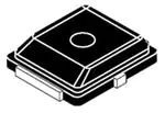
CASE 466 - 03, STYLE 1
PLD - 1.5
PLASTIC
Table 1. Maximum Ratings
Rating
Symbol
Value
Unit
Drain- Source Voltage
VDSS
15
Vdc
Gate- Source Voltage
VGS
-5
Vdc
RF Input Power
Pin
30
dBm
Storage Temperature Range
Tstg
- 65 to +150
°C
Channel Temperature (1)
Tch
175
°C
Symbol
Value (2)
Unit
RθJC
13.7
°C/W
Table 2. Thermal Characteristics
Characteristic
Thermal Resistance, Junction to Case
Table 3. ESD Protection Characteristics
Test Methodology
Class
Human Body Model (per JESD22 - A114)
1C (Minimum)
Machine Model (per EIA/JESD22 - A115)
A (Minimum)
Charge Device Model (per JESD22 - C101)
IV (Minimum)
Table 4. Moisture Sensitivity Level
Test Methodology
Per JESD22 - A113, IPC/JEDEC J - STD - 020
Rating
Package Peak Temperature
Unit
3
260
°C
1. For reliable operation, the operating channel temperature should not exceed 150°C.
2. Refer to AN1955, Thermal Measurement Methodology of RF Power Amplifiers. Go to http://www.freescale.com/rf.
Select Documentation/Application Notes - AN1955.
© Freescale Semiconductor, Inc., 2007 - 2009. All rights reserved.
RF Device Data
Freescale Semiconductor
MRFG35005ANT1
1
�Table 5. Electrical Characteristics (TA = 25°C unless otherwise noted)
Characteristic
Symbol
Min
Typ
Max
Unit
Saturated Drain Current
(VDS = 3.5 Vdc, VGS = 0 Vdc)
IDSS
—
1.7
—
Adc
Off State Leakage Current
(VGS = - 0.4 Vdc, VDS = 0 Vdc)
IGSS
—
很抱歉,暂时无法提供与“MRFG35005ANT1”相匹配的价格&库存,您可以联系我们找货
免费人工找货