Freescale Semiconductor
Technical Data
Document Number: MRFG35010
Rev. 9, 1/2008
MRFG35010R1 replaced by MRFG35010AR1.
MRFG35010R1
Gallium Arsenide PHEMT
RF Power Field Effect Transistor
3.5 GHz, 10 W, 12 V
POWER FET
GaAs PHEMT
• Typical W - CDMA Performance: - 42 dBc ACPR, 3.55 GHz, 12 Volts,
IDQ = 180 mA, 5 MHz Offset/3.84 MHz BW, 64 DPCH (8.5 dB P/A
@ 0.01% Probability)
Output Power — 1 Watt
Power Gain — 10 dB
Efficiency — 30%
• 10 Watts P1dB @ 3550 MHz
• Excellent Phase Linearity and Group Delay Characteristics
• High Gain, High Efficiency and High Linearity
• RoHS Compliant
• In Tape and Reel. R1 Suffix = 500 Units per 32 mm, 13 inch Reel.
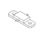
CASE 360D - 02, STYLE 1
NI - 360HF
Table 1. Maximum Ratings
Rating
Symbol
Value
Unit
VDSS
15
Vdc
Total Device Dissipation @ TC = 25°C
Derate above 25°C
PD
28.3
0.19
W
W/°C
Gate - Source Voltage
VGS
-5
Vdc
RF Input Power
Pin
33
dBm
Tstg
- 65 to +175
°C
Tch
175
°C
TC
- 20 to +90
°C
Symbol
Value
Unit
RθJC
5.3
4.8
°C/W
Drain - Source Voltage
Storage Temperature Range
Channel Temperature
(1)
Operating Case Temperature Range
ARCHIVE INFORMATION
ARCHIVE INFORMATION
Designed for WLL/MMDS or UMTS driver applications with frequencies from
1800 to 3600 MHz. Device is unmatched and is suitable for use in Class AB or
Class A linear base station applications.
Table 2. Thermal Characteristics
Characteristic
Thermal Resistance, Junction to Case
Class A
Class AB
1. For reliable operation, the operating channel temperature should not exceed 150°C.
© Freescale Semiconductor, Inc., 2008. All rights reserved.
RF Device Data
Freescale Semiconductor
MRFG35010R1
1
�Characteristic
ARCHIVE INFORMATION
Symbol
Min
Typ
Max
Unit
Saturated Drain Current
(VDS = 3.5 Vdc, VGS = 0 Vdc)
IDSS
—
2.9
—
Adc
Off State Leakage Current
(VGS = - 0.4 Vdc, VDS = 0 Vdc)
IGSS
—
很抱歉,暂时无法提供与“MRFG35010”相匹配的价格&库存,您可以联系我们找货
免费人工找货