NT3H1101/NT3H1201
NTAG I2C - Energy harvesting NFC Forum Type 2 Tag with
field detection pin and I2C interface
Rev. 3.3 — 15 July 2015
265433
Product data sheet
COMPANY PUBLIC
1. General description
NTAG I2C - The entry to the NFC world: simple and lowest cost.
The NTAG I2C is the first product of NXP’s NTAG family offering both contactless and
contact interfaces (see Figure 1). In addition to the passive NFC Forum compliant
contactless interface, the IC features an I2C contact interface, which can communicate
with a microcontroller if the NTAG I2C is powered from an external power supply. An
additional externally powered SRAM mapped into the memory allows a fast data transfer
between the RF and I2C interfaces and vice versa, without the write cycle limitations of the
EEPROM memory.
The NTAG I2C product features a configurable field detection pin, which provides a trigger
to an external device depending on the activities at the RF interface.
The NTAG I2C product can also supply power to external (low power) devices (e.g. a
microcontroller) via the embedded energy harvesting circuitry.
I2C
EEPROM
1 0 1 0 1 0
NFC
enabled
device
Micro
controller
Energy Harvesting
Data
Energy
Field detection
Data
Energy
aaa-010357
Fig 1.
Contactless and contact system
�NT3H1101/NT3H1201
NXP Semiconductors
NTAG I2C - Energy harvesting Type 2 Tag with I2C interface
2. Features and benefits
2.1 Key features
RF interface NFC Forum Type 2 Tag compliant
I2C interface
Configurable field detection pin based on open drain implementation that can be
triggered upon the following events:
RF field presence
First start of communication
Selection of the tag only
64 byte SRAM buffer for fast transfer of data (Pass-through mode) between the RF
and the I2C interfaces located outside the User Memory
Wake up signal at the field detect pin when:
New data has arrived from one interface
Data has been read by the receiving interface
Clear arbitration between RF and I2C interfaces:
First come, first serve strategy
Status flag bits to signal if one interface is busy writing to or reading data from the
EEPROM
Energy harvesting functionality to power external devices (e.g. microcontroller)
FAST READ command for faster data reading
2.2 RF interface
Contactless transmission of data
NFC Forum Type 2 Tag compliant (see Ref. 1)
Operating frequency of 13.56 MHz
Data transfer of 106 kbit/s
4 bytes (one page) written including all overhead in 4.8 ms via EEPROM or 0.8 ms via
SRAM (Pass-through mode)
Data integrity of 16-bit CRC, parity, bit coding, bit counting
Operating distance of up to 100 mm (depending on various parameters, such as field
strength and antenna geometry)
True anticollision
Unique 7 byte serial number (cascade level 2 according to ISO/IEC 14443-3
(see Ref. 2)
2.3 Memory
1904 bytes freely available with User Read/Write area (476 pages with 4 bytes per
pages) for the NTAG I2C 2k version
888 bytes freely available with User Read/Write area (222 pages with 4 bytes per
pages) for the NTAG I2C 1k version
Field programmable RF read-only locking function with static and dynamic lock bits
configurable from both I²C and NFC interfaces
64 bytes SRAM volatile memory without write endurance limitation
NT3H1101/1201
Product data sheet
COMPANY PUBLIC
All information provided in this document is subject to legal disclaimers.
Rev. 3.3 — 15 July 2015
265433
© NXP Semiconductors N.V. 2015. All rights reserved.
2 of 65
�NT3H1101/NT3H1201
NXP Semiconductors
NTAG I2C - Energy harvesting Type 2 Tag with I2C interface
Data retention time of 20 years
Write endurance 500,000 cycles
2.4 I2C interface
I2C slave interface supports Standard (100 kHz) and Fast (up to 400 kHz) mode (see
Ref. 3)
16 bytes (one block) written in 4.5 ms (EEPROM) or 0.4 ms (SRAM - Pass-through
mode) including all overhead
RFID chip can be used as standard I2C EEPROM
2.5 Security
Manufacturer-programmed 7-byte UID for each device
Capability container with one time programmable bits
Field programmable read-only locking function per page for first 12 pages and per 16
(1k version) or 32 (2k version) pages for the extended memory section
2.6 Key benefits
The Pass-through mode allows fast download and upload of data from RF to I²C and
vice versa without the cycling limitation of EEPROM
NDEF message storage up to 1904 bytes (2k version) or up to 888 bytes (1k version)
The mapping of the SRAM inside the User Memory buffer allows dynamic update of
NDEF message content
3. Applications
With all its integrated features and functions the NTAG I2C is the ideal solution to enable a
contactless communication via an NFC device (e.g., NFC enabled mobile phone) to an
electronic device for:
Zero power configuration (late customization)
Smart customer interaction (e.g., easier after sales service, such as firmware update)
Advanced pairing (for e.g., WiFi or Blue tooth) for dynamic generation of sessions keys
Easier product customization and customer experience for the following applications:
Home automation
Home appliances
Consumer electronics
Healthcare
Printers
Smart meters
NT3H1101/1201
Product data sheet
COMPANY PUBLIC
All information provided in this document is subject to legal disclaimers.
Rev. 3.3 — 15 July 2015
265433
© NXP Semiconductors N.V. 2015. All rights reserved.
3 of 65
�NT3H1101/NT3H1201
NXP Semiconductors
NTAG I2C - Energy harvesting Type 2 Tag with I2C interface
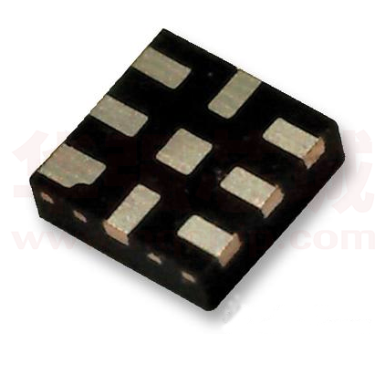
4. Ordering information
Table 1.
Ordering information
Type number
Package
Name
Description
Version
FFC
bumped
8 inch wafer, 150um thickness, on film frame carrier, electronic fail die
-
FFC
bumped
8 inch wafer, 150um thickness, on film frame carrier, electronic fail die
NT3H1101W0FHK
XQFN8
Plastic, extremely thin quad flat package; no leads; 8 terminals; body 1.6 x
1.6 x 0.6mm; 1k bytes memory, 50pF input capacitance
SOT902-3
NT3H1201W0FHK
XQFN8
Plastic, extremely thin quad flat package; no leads; 8 terminals; body 1.6 x
1.6 x 0.6mm; 2k bytes memory, 50pF input capacitance
SOT902-3
NT3H1101W0FTT
TSSOP8
Plastic thin shrink small outline package; 8 leads; body width 3 mm; 1k
bytes memory; 50pF input capacitance
SOT505-1
NT3H1201W0FTT
TSSOP8
Plastic thin shrink small outline package; 8 leads; body width 3 mm; 2k
bytes memory; 50pF input capacitance
SOT505-1
NT3H1101W0FUG
NT3H1201W0FUG
marking according to SECS-II format), Au bumps, 1k Bytes memory, 50pF
input capacitance
-
marking according to SECS-II format), Au bumps, 2k Bytes memory, 50pF
input capacitance
5. Marking
Table 2.
NT3H1101/1201
Product data sheet
COMPANY PUBLIC
Marking codes
Type number
Marking code
NT3H1201FHK
N12
NT3H1101FHK
N11
NT3H1101W0FFT
31101
NT3H1201W0FFT
31201
All information provided in this document is subject to legal disclaimers.
Rev. 3.3 — 15 July 2015
265433
© NXP Semiconductors N.V. 2015. All rights reserved.
4 of 65
�NT3H1101/NT3H1201
NXP Semiconductors
NTAG I2C - Energy harvesting Type 2 Tag with I2C interface
6. Block diagram
VCC
LA
RF
INTERFACE
GND
Vout
POWER MANAGEMENT/
ENERGY HARVESTING
I2C
SLAVE
DIGITAL CONTROL UNIT
MEMORY
ARBITER/STATUS
REGISTERS
SDA
I2C
CONTROL
EEPROM
LB
SCL
ANTICOLLISION
COMMAND
INTERPRETER
MEMORY
INTERFACE
SRAM
FD
aaa-010358
Fig 2.
NT3H1101/1201
Product data sheet
COMPANY PUBLIC
Block diagram
All information provided in this document is subject to legal disclaimers.
Rev. 3.3 — 15 July 2015
265433
© NXP Semiconductors N.V. 2015. All rights reserved.
5 of 65
�NT3H1101/NT3H1201
NXP Semiconductors
NTAG I2C - Energy harvesting Type 2 Tag with I2C interface
7. Pinning information
7.1 Pinning
7.1.1 XQFN8
A
LB
8
A
LA
1
7
VOUT
VSS
2
6
VCC
SCL
3
5
SDA
4
FD
Transparent top view
B
side view
aaa-010359
(1) Dimension A: 1.6 mm
(2) Dimension B: 0.5 mm
Fig 3.
Pin configuration for XQFN8
7.1.2 TSSOP8
8 LB
LA 1
VSS 2
7 VOUT
SCL 3
6 VCC
FD 4
5 SDA
B
A
C
Transparent top view
Side view
aaa-017246
(1) Dimension A: 5.1 mm
(2) Dimension B: 3.1 mm
(3) Dimension C: 1.1 mm
Fig 4.
NT3H1101/1201
Product data sheet
COMPANY PUBLIC
Pin configuration for TSSOP8
All information provided in this document is subject to legal disclaimers.
Rev. 3.3 — 15 July 2015
265433
© NXP Semiconductors N.V. 2015. All rights reserved.
6 of 65
�NT3H1101/NT3H1201
NXP Semiconductors
NTAG I2C - Energy harvesting Type 2 Tag with I2C interface
7.2 Pin description
Table 3.
Pin description for XQFN8 and TSSOP8
Pin
Symbol
Description
1
LA
Antenna connection LA
2
VSS
GND
3
SCL
Serial Clock I2C
4
FD
Field detection
5
SDA
Serial data I2C
6
VCC
VCC in connection (external power supply)
7
VOUT
Voltage out (energy harvesting)
8
LB
Antenna connection LB
NXP recommends leaving the central pad of the XQFN8 package unconnected.
NT3H1101/1201
Product data sheet
COMPANY PUBLIC
All information provided in this document is subject to legal disclaimers.
Rev. 3.3 — 15 July 2015
265433
© NXP Semiconductors N.V. 2015. All rights reserved.
7 of 65
�NT3H1101/NT3H1201
NXP Semiconductors
NTAG I2C - Energy harvesting Type 2 Tag with I2C interface
8. Functional description
8.1 Block description
NTAG I2C ICs consist of (see details below): 2016 bytes of EEPROM memory, 64 Bytes of
SRAM, a RF interface, Digital Control Unit (DCU), Power Management Unit (PMU) and an
I²C interface. Energy and data are transferred via an antenna consisting of a coil with a
few turns, which is directly connected to NTAG I2C IC.
• RF interface:
– modulator/demodulator
– rectifier
– clock regenerator
– Power-On Reset (POR)
– voltage regulator
• Anticollision: multiple cards may be selected and managed in sequence
• Command interpreter: processes memory access commands supported by the NTAG
I2C
• EEPROM interface
8.2 RF interface
The RF-interface is based on the ISO/IEC 14443 Type A standard.
This RF interface is passive and therefore requires to be supplied by an RF field (e.g. NFC
enabled device) at all times to be able to operate. It is not operating even if the NTAG I2C
is powered via its contact interface (Vcc).
Data transmission from the RF interface is only happening if RF field from an NFC
enabled device is available and adequate commands are sent to retrieve data from the
NTAG I2C.
For both directions of data communication, there is one start bit (start of communication)
at the beginning of each frame. Each byte is transmitted with an odd parity bit at the end.
The LSB of the byte with the lowest address of the selected block is transmitted first.
The maximum length of an NFC device to tag frame used in this product is 82 bits (7 data
bytes + 2 CRC bytes = 7×9 + 2×9 + 1 start bit).
The maximum length of a tag to NFC device frame (response to READ command) is 163
bits (16 data bytes + 2 CRC bytes = 16 9 + 2 9 + 1 start bit).
In addition the proprietary FAST_READ command has a variable response frame length,
which depends on the start and end address parameters. E.g. when reading the SRAM at
once the length of the response is 595 bits (64 data bytes + 2 CRC bytes = 64 9 + 2 9
+ 1 start bit). The overall maximum supported response frame length for FAST READ is
up to 9235 bits (1024 data bytes + 2 CRC bytes = 1024 9 + 2 9 + 1 start bit), but here
the maximum frame length supported by the NFC device must be taken into account
when issuing this command.
NT3H1101/1201
Product data sheet
COMPANY PUBLIC
All information provided in this document is subject to legal disclaimers.
Rev. 3.3 — 15 July 2015
265433
© NXP Semiconductors N.V. 2015. All rights reserved.
8 of 65
�NT3H1101/NT3H1201
NXP Semiconductors
NTAG I2C - Energy harvesting Type 2 Tag with I2C interface
For a multi-byte parameter, the least significant byte is always transmitted first. For
example, when reading from the memory using the READ command, byte 0 from the
addressed block is transmitted first, followed by bytes 1 to byte 3 out of this block. The
same sequence continues for the next block and all subsequent blocks.
8.2.1 Data integrity
The following mechanisms are implemented in the contactless communication link
between the NFC device and the NTAG I²C IC to ensure very reliable data transmission:
•
•
•
•
•
16 bits CRC per block
Parity bits for each byte
Bit count checking
Bit coding to distinguish between “1”, “0” and “no information”
Channel monitoring (protocol sequence and bit stream analysis)
The commands are initiated by the NFC device and controlled by the Digital Control Unit
of the NTAG I2C IC. The command response depends on the state of the IC, and for
memory operations, also on the access conditions valid for the corresponding page.
NT3H1101/1201
Product data sheet
COMPANY PUBLIC
All information provided in this document is subject to legal disclaimers.
Rev. 3.3 — 15 July 2015
265433
© NXP Semiconductors N.V. 2015. All rights reserved.
9 of 65
�NT3H1101/NT3H1201
NXP Semiconductors
NTAG I2C - Energy harvesting Type 2 Tag with I2C interface
8.2.2 RF communication principle
POR
HALT
IDLE
REQA
WUPA
WUPA
READY 1
identification
and
selection
procedure
ANTICOLLISION
SELECT
cascade level 1
HLTA
READY 2
ANTICOLLISION
SELECT
cascade level 2
ACTIVE
READ (16 Byte)
FAST_READ
WRITE
SECTOR_SELECT
GET_VERSION
memory
operations
aaa-012797
Fig 5.
RF communication principle of NTAG I2C
The overall RF communication principle is summarized in Figure 5.
8.2.2.1
IDLE state
After a power-on reset (POR), the NTAG I2C switches to the IDLE state. It only exits this
state when a REQA or a WUPA command is received from the NFC device. Any other
data received while in this state is interpreted as an error, and the NTAG I2C remains in
the IDLE state.
After a correctly executed HLTA command e.g., out of the ACTIVE state, the default
waiting state changes from the IDLE state to the HALT state. This state can then only be
exited with a WUPA command.
8.2.2.2
READY 1 state
In the READY 1 state, the NFC device resolves the first part of the UID (3 bytes) using the
ANTICOLLISION or SELECT commands in cascade level 1. This state is correctly exited
after execution of the following command:
• SELECT command from cascade level 1: the NFC device switches the NTAG I2C into
READY2 state where the second part of the UID is resolved.
NT3H1101/1201
Product data sheet
COMPANY PUBLIC
All information provided in this document is subject to legal disclaimers.
Rev. 3.3 — 15 July 2015
265433
© NXP Semiconductors N.V. 2015. All rights reserved.
10 of 65
�NT3H1101/NT3H1201
NXP Semiconductors
NTAG I2C - Energy harvesting Type 2 Tag with I2C interface
8.2.2.3
READY 2 state
In the READY 2 state, the NTAG I2C supports the NFC device in resolving the second part
of its UID (4 bytes) with the cascade level 2 ANTICOLLISION command. This state is
usually exited using the cascade level 2 SELECT command.
Remark: The response of the NTAG I2C to the SELECT command is the Select
AcKnowledge (SAK) byte. In accordance with ISO/IEC 14443, this byte indicates if the
anticollision cascade procedure has finished. If finished, the NTAG I2C is now uniquely
selected and only this device will communicate with the NFC device even when other
contactless devices are present in the NFC device field.
8.2.2.4
ACTIVE state
All memory operations are operated in the ACTIVE state.
The ACTIVE state is exited with the HLTA command and upon reception, the NTAG I2C
transits to the HALT state. Any other data received when the device is in this state is
interpreted as an error. Depending on its previous state, the NTAG I2C returns to either to
the IDLE state or HALT state.
8.2.2.5
HALT state
HALT and IDLE states constitute the two wait states implemented in the NTAG I2C. An
already processed NTAG I2C can be set into the HALT state using the HLTA command. In
the anticollision phase, this state helps the NFC device distinguish between processed
tags and tags yet to be selected. The NTAG I2C can only exit this state upon execution of
the WUPA command. Any other data received when the device is in this state is
interpreted as an error, and NTAG I2C state remains unchanged.
8.3 Memory organization
The memory map is detailed in Table 4 (1k memory) and Table 5 (2k memory) from the
RF interface and in Table 6 (1k memory) and Table 7 (2k memory) from the I2C interface.
The SRAM memory is not mapped from the RF interface, because in the default settings
of the NTAG I2C the Pass-through mode is not enabled. Please refer to Section 11 for
examples of memory map from the RF interface with SRAM mapping.
The structure of manufacturing data, static lock bytes, capability container and user
memory pages (except of the user memory length) are compatible with other NTAG
products.
Any memory access which starts at a valid address and extends into an invalid access
region will return 00h value in the invalid region.
8.3.1 Memory map from RF interface
Memory access from the RF interface is organized in pages of 4 bytes each.
NT3H1101/1201
Product data sheet
COMPANY PUBLIC
All information provided in this document is subject to legal disclaimers.
Rev. 3.3 — 15 July 2015
265433
© NXP Semiconductors N.V. 2015. All rights reserved.
11 of 65
�NT3H1101/NT3H1201
NXP Semiconductors
NTAG I2C - Energy harvesting Type 2 Tag with I2C interface
Table 4.
Sector
address
0
NT3H1101/1201
Product data sheet
COMPANY PUBLIC
NTAG I2C 1k memory organization from the RF interface
Page address
Dec.
Hex.
0
00h
1
01h
2
02h
3
03h
4
04h
...
...
15
0Fh
...
...
225
E1h
226
E2h
227
E3h
228
E4h
229
E5h
230
E6h
231
E7h
232
E8h
233
E9h
234
EAh
...
...
255
FFh
1
...
2
3
Byte number within a page
0
1
2
3
Access
conditions
Internal
READ
Serial number
READ
Serial number
Internal
Static lock bytes
READ/R&W
Capability Container (CC)
READ&WRITE
User memory
READ&WRITE
Dynamic lock bytes
00h
R&W/READ
Invalid access - returns NAK
n.a.
Configuration registers
see 8.3.11
Invalid access - returns NAK
n.a.
...
Invalid access - returns NAK
n.a.
...
...
Invalid access - returns NAK
n.a.
0
00h
...
...
Invalid access - returns NAK
n.a.
248
F8h
249
F9h
Session registers
see 8.3.11
...
...
255
FFh
Invalid access - returns NAK
n.a.
All information provided in this document is subject to legal disclaimers.
Rev. 3.3 — 15 July 2015
265433
© NXP Semiconductors N.V. 2015. All rights reserved.
12 of 65
�NT3H1101/NT3H1201
NXP Semiconductors
NTAG I2C - Energy harvesting Type 2 Tag with I2C interface
Table 5.
Sector
address
0
1
NTAG I2C 2k memory organization from the RF interface
Page address
Dec.
Hex.
0
00h
1
01h
2
02h
3
03h
4
04h
...
...
15
0Fh
...
...
...
...
255
FFh
0
...
1
...
...
...
...
...
223
DFh
224
E0h
225
E1h
226
E2h
227
E3h
228
E4h
229
E5h
230
E6h
231
E7h
232
E8h
233
E9h
234
EAh
...
...
255
FFh
2
...
...
3
0
00h
...
...
248
F8h
249
F9h
...
...
255
FFh
Byte number within a page
0
1
2
3
Access
conditions
Internal
READ
Serial number
READ
Serial number
Internal
Static lock bytes
READ/R&W
Capability Container (CC)
READ&WRITE
User memory
READ&WRITE
Dynamic lock bytes
00h
R&W/READ
Invalid access - returns NAK
n.a.
Configuration registers
see 8.3.11
Invalid access - returns NAK
n.a.
Invalid access - returns NAK
n.a.
Invalid access - returns NAK
n.a.
Session registers
see 8.3.11
Invalid access - returns NAK
n.a.
8.3.2 Memory map from I²C interface
The memory access of NTAG I²C from the I²C interface is organized in blocks of 16 bytes
each.
NT3H1101/1201
Product data sheet
COMPANY PUBLIC
All information provided in this document is subject to legal disclaimers.
Rev. 3.3 — 15 July 2015
265433
© NXP Semiconductors N.V. 2015. All rights reserved.
13 of 65
�NT3H1101/NT3H1201
NXP Semiconductors
NTAG I2C - Energy harvesting Type 2 Tag with I2C interface
Table 6.
NTAG I2C 1k memory organization from the I2C interface
Byte number within a block
I2C block
address
Dec.
0
Hex.
00h
I2C
0
1
2
3
4
5
6
7
8
9
10
11
12
13
14
15
addr.*
Serial number
Serial number
Internal
1
...
...
37h
56
38h
Internal
Static lock bytes
READ
READ/R&W
Capability Container (CC)
READ&WRITE
User memory
READ&WRITE
User memory
READ&WRITE
User memory
READ&WRITE
Dynamic lock bytes
00h
58
R&W/READ
01h
55
57
Access
conditions
00h
00h
00h
READ&WRITE
00h
READ
39h
3Ah
59
3Bh
...
...
247
F7h
248
F8h
...
...
251
FBh
Invalid access - returns NAK
n.a.
Configuration registers
see 8.3.11
00h
00h
00h
00h
00h
00h
00h
00h
READ
Invalid access - returns NAK
n.a.
SRAM memory (64 bytes)
READ&WRITE
...
...
Invalid access - returns NAK
n.a.
254
FEh
Session registers
(requires READ register command)
see 8.3.11
...
...
00h
00h
00h
00h
00h
00h
00h
00h
Invalid access - returns NAK
READ
n.a.
Remark: * The byte 0 of block 0 is always read as 04h. Writing to this byte modifies the I2C
address.
NT3H1101/1201
Product data sheet
COMPANY PUBLIC
All information provided in this document is subject to legal disclaimers.
Rev. 3.3 — 15 July 2015
265433
© NXP Semiconductors N.V. 2015. All rights reserved.
14 of 65
�NT3H1101/NT3H1201
NXP Semiconductors
NTAG I2C - Energy harvesting Type 2 Tag with I2C interface
Table 7.
NTAG I2C 2k memory organization from the I2C interface
Byte number within a block
I2C block
address
Dec.
0
Hex.
00h
I2C
0
1
2
3
4
5
6
7
8
9
10
11
12
13
14
15
addr.*
Serial number
Serial number
Internal
1
...
...
77h
120
78h
122
R&W/READ
Internal
Static lock bytes
READ
READ/R&W
Capability Container (CC)
READ&WRITE
User memory
READ&WRITE
01h
119
121
Access
conditions
Dynamic lock bytes
00h
00h
00h
00h
00h
00h
00h
00h
00h
00h
00h
00h
00h
READ&WRITE
READ
79h
7Ah
127
7Bh
...
...
247
F7h
248
F8h
...
...
251
FBh
Invalid access - returns NAK
n.a.
Configuration registers
see 8.3.11
00h
00h
00h
00h
00h
00h
00h
00h
READ
Invalid access - returns NAK
n.a.
SRAM memory (64 bytes)
READ&WRITE
...
...
Invalid access - returns NAK
n.a.
254
FEh
Session registers
(requires READ register command)
see 8.3.11
...
...
00h
00h
00h
00h
00h
00h
00h
00h
Invalid access - returns NAK
READ
n.a.
Remark: * The byte 0 of block 0 is always read as 04h. Writing to this byte modifies the I2C
address.
NT3H1101/1201
Product data sheet
COMPANY PUBLIC
All information provided in this document is subject to legal disclaimers.
Rev. 3.3 — 15 July 2015
265433
© NXP Semiconductors N.V. 2015. All rights reserved.
15 of 65
�NT3H1101/NT3H1201
NXP Semiconductors
NTAG I2C - Energy harvesting Type 2 Tag with I2C interface
8.3.3 EEPROM
The EEPROM is a non volatile memory that stores the 7 byte UID, the memory lock
conditions, IC configuration information and the 1904 bytes user data (888 byte user data
in case of the NTAG I2C 1k version).
8.3.4 SRAM
For frequently changing data, a volatile memory of 64 bytes with unlimited endurance is
built in. The 64 bytes are mapped in a similar way as done in the EEPROM, i.e., 64 bytes
are seen as 16 pages of 4 bytes.
The SRAM is only available if the tag is powered via the VCC pin.
The SRAM is located at the end of the memory space and it is always directly accessible
by the I2C host (addresses F8h to FBh). An RF reader cannot access the SRAM memory
in normal mode (i.e., outside the Pass-through mode). The SRAM is only accessible by
the RF reader if the SRAM is mirrored onto the EEPROM memory space.
With Memory Mirror enabled (SRAM_MIRROR_ON_OFF = 1b - see Section 11.2), the
SRAM can be mirrored in the User Memory (page 1 to page 116 - see Section 11.2) for
access from the RF side.
The Memory mirror must be enabled once both interfaces are ON as this feature is
disabled after each POR.
The register SRAM_MIRROR_BLOCK (see Table 14) indicates the address of the first
page of the SRAM buffer. In the case where the SRAM mirror is enabled and the READ
command is addressing blocks where the SRAM mirror is located, the SRAM mirror byte
values will be returned instead of the EEPROM byte values. Similarly, if the tag is not VCC
powered, the SRAM mirror is disabled and reading out the bytes related to the SRAM
mirror position would return the values from the EEPROM.
In the Pass-through mode (PTHRU_ON_OFF = 1b - see Section 8.3.11), the SRAM is
mirrored to the fixed address 240 - 255 for RF access (see Section 11) in the first memory
sector for NTAG I2C 1k and in the second memory sector for NTAG I2C 2k.
8.3.5 UID/serial number
The unique 7-byte serial number (UID) is programmed into the first 7 bytes of memory
covering page addresses 00h and 01h - see Figure 6. These bytes are programmed and
write protected in the production test.
SN0 holds the Manufacturer ID for NXP Semiconductors (04h) in accordance with
ISO/IEC 14443-3.
NT3H1101/1201
Product data sheet
COMPANY PUBLIC
All information provided in this document is subject to legal disclaimers.
Rev. 3.3 — 15 July 2015
265433
© NXP Semiconductors N.V. 2015. All rights reserved.
16 of 65
�NT3H1101/NT3H1201
NXP Semiconductors
NTAG I2C - Energy harvesting Type 2 Tag with I2C interface
MSB
0
LSB
0
0
0
0
1
0
0
manufacturer ID for NXP Semiconductors (04h)
page 0
page 1
byte UID0 UID1 UID2 UID3
page 2
0
UID4 UID5 UID6 SAK
7 bytes UID
1
2
3
ATQA0
ATQA1
lock bytes
aaa-012802
Fig 6.
UID/serial number
8.3.6 Static lock bytes
The bits of byte 2 and byte 3 of page 02h (via RF) or byte 10 and 11 address 0h (via I2C)
represent the field programmable, read-only locking mechanism (see Figure 7). Each
page from 03h (CC) to 0Fh can be individually locked by setting the corresponding locking
bit Lx to logic 1 to prevent further write access. After locking, the corresponding page
becomes read-only memory.
The three least significant bits of lock byte 0 are the block-locking bits. Bit 2 controls
pages 0Ah to 0Fh (via RF), bit 1 controls pages 04h to 09h (via RF) and bit 0 controls
page 03h (CC). Once the block-locking bits are set, the locking configuration for the
corresponding memory area is frozen.
MSB
L
7
L
6
L
5
L
4
L
CC
BL
15-10
LSB
MSB
BL
CC
L
15
BL
9-4
LSB
L
14
L
13
L
12
L
11
L
10
L
9
L
8
page 2
0
1
2
3
lock byte 0
lock byte 1
Fig 7.
Lx locks page x to read-only
BLx blocks further locking for the memory area x
aaa-006983
Static lock bytes 0 and 1
For example, if BL15-10 is set to logic 1, then bits L15 to L10 (lock byte 1, bit[7:2]) can no
longer be changed. The static locking and block-locking bits are set by the bytes 2 and 3
of the WRITE command to page 02h. The contents of the lock bytes are bit-wise OR’ed
and the result then becomes the new content of the lock bytes.
This process is irreversible from RF perspective. If a bit is set to logic 1, it cannot be
changed back to logic 0. From I²C perspective, the bits can be reset to 0b by writing bytes
10 and 11 of block 0. I²C address is coded in byte 0 of block 0 and may be changed
unintentionally.
The contents of bytes 0 and 1 of page 02h are unaffected by the corresponding data bytes
of the WRITE.
The default value of the static lock bytes is 00 00h.
NT3H1101/1201
Product data sheet
COMPANY PUBLIC
All information provided in this document is subject to legal disclaimers.
Rev. 3.3 — 15 July 2015
265433
© NXP Semiconductors N.V. 2015. All rights reserved.
17 of 65
�NT3H1101/NT3H1201
NXP Semiconductors
NTAG I2C - Energy harvesting Type 2 Tag with I2C interface
8.3.7 Dynamic Lock Bytes
To lock the pages of NTAG I2C starting at page address 10h and onwards, the dynamic
lock bytes are used. The dynamic lock bytes are located at page E2h sector 0 (NTAG I2C
1k) or address E0h sector 1 (NTAG I2C 2k). The three lock bytes cover the memory area
of 830 data bytes (NTAG I2C 1k) or 1846 data bytes (NTAG I2C 2k). The granularity is 16
pages for NTAG I2C 1k (see Figure 8) and 32 pages for NTAG I2C 2k (see Figure 9)
compared to a single page for the first 48 bytes (see Figure 7).
Remark: Set all bits marked with RFUI to 0 when writing to the dynamic lock bytes.
LOCK PAGE
64-79
LOCK PAGE
48-63
LOCK PAGE
32-47
LOCK PAGE
16-31
RFUI
RFUI
LOCK PAGE
224-225
LOCK PAGE
208-223
LOCK PAGE
192-207
LOCK PAGE
176-191
LOCK PAGE
160-175
LOCK PAGE
144-159
LSB
LOCK PAGE
80-95
MSB
LOCK PAGE
96-111
bit 7
LSB
LOCK PAGE
112-127
LOCK PAGE
128-143
MSB
6
5
4
3
2
1
0
bit 7
6
5
4
3
2
1
0
page 226 (E2h)
0
1
2
3
BL 208-225
BL 176-207
BL 144-175
BL 112-143
BL 80-111
BL 48-79
BL 16-47
LSB
RFUI
MSB
bit 7
6
5
4
3
2
1
0
aaa-008092
Fig 8.
NT3H1101/1201
Product data sheet
COMPANY PUBLIC
NTAG I2C 1k Dynamic lock bytes 0, 1 and 2
All information provided in this document is subject to legal disclaimers.
Rev. 3.3 — 15 July 2015
265433
© NXP Semiconductors N.V. 2015. All rights reserved.
18 of 65
�NT3H1101/NT3H1201
NXP Semiconductors
NTAG I2C - Energy harvesting Type 2 Tag with I2C interface
LOCK PAGE
144-175
LOCK PAGE
112-143
LOCK PAGE
80-111
LOCK PAGE
48-79
LOCK PAGE
16-47
RFUI
LOCK PAGE
464-479
LOCK PAGE
432-463
LOCK PAGE
400-431
LOCK PAGE
368-399
LOCK PAGE
336-367
LOCK PAGE
304-335
LOCK PAGE
272-303
LSB
LOCK PAGE
176-207
MSB
LOCK PAGE
208-239
LSB
LOCK PAGE
240-271
MSB
bit 7
6
5
4
3
2
1
0
bit 7
6
5
4
3
2
1
0
page 224 (E0h)
0
1
2
3
BL 400-463
BL 336-399
BL 272-335
BL 208-271
BL 144-207
BL 80-143
BL 16-79
LSB
BL 464-479
MSB
bit 7
6
5
4
3
2
1
0
Block Locking (BL) bits
aaa-012803
Fig 9.
NTAG I2C 2k Dynamic lock bytes 0, 1 and 2
The default value of the dynamic lock bytes is 00 00 00h. The value of Byte 3 is always
00h when read.
Reading the 3 bytes for the dynamic lock bytes and the Byte 3 (00h) from RF interface
(address E2h sector 0 (NTAG I2C 1k) or E0h sector 1 (NTAG I2C 2k) or from I2C (address
38h (NTAG I2C 1k) or 78h (NTAG I2C 2k)) will also return a fixed value for the next 12
bytes of 00h.
Like for the static lock bytes, this process of modifying the dynamic lock bytes is
irreversible from RF perspective. If a bit is set to logic 1, it cannot be changed back to
logic 0. From I²C perspective, the bits can be reset to 0b.
NT3H1101/1201
Product data sheet
COMPANY PUBLIC
All information provided in this document is subject to legal disclaimers.
Rev. 3.3 — 15 July 2015
265433
© NXP Semiconductors N.V. 2015. All rights reserved.
19 of 65
�NT3H1101/NT3H1201
NXP Semiconductors
NTAG I2C - Energy harvesting Type 2 Tag with I2C interface
8.3.8 Capability Container (CC bytes)
The Capability Container CC (page 03h) is programmed during the IC production
according to the NFC Forum Type 2 Tag specification (see Ref. 1). These bytes may be
bit-wise modified by a WRITE command from the I²C or RF interface. Once set to 1b, it is
only possible to reset it to 0b from I²C perspective. I²C address (byte 0) and static lock
bytes (byte 10 and byte 11) are coded in block 0 and may be changed unintentionally.
See examples for NTAG I2C 1k version in Figure 10 and for NTAG I2C 2k version in
Figure 11.
page 3
byte
0
1
2
3
byte E1h 10h 6Dh 00h
Example NTAG I2C 1k version
default value (initialized state)
11100001
00010000
CC bytes
01101101
00000000
00000000
00001111
write command to page 3
CC bytes
00000000
00000000
result in page 3 (read-only state)
11100001
00010000
01101101
00001111
aaa-012804
Fig 10. CC bytes of NTAG I2C 1k version
page 3
byte
0
1
2
3
data E1h 10h EAh 00h
Example NTAG I2C 2k version
default value (initialized state)
11100001
00010000
CC bytes
11101010
00000000
00000000
00001111
write command to page 3
CC bytes
00000000
00000000
result in page 3 (read-only state)
11100001
00010000
11101010
00001111
aaa-012805
Fig 11. CC bytes of NTAG I2C 2k version
The default values of the CC bytes at delivery are defined in Section 8.3.10.
8.3.9 User Memory pages
Pages 04h to E1h via the RF interface - Block 01h to 37h, plus the first 8 bytes of block
38h via the I2C interface are the user memory read/write areas for NTAG I2C 1k version.
Pages 04h (sector 0) to DFh (sector 1) via the RF interface - Block 1h to 77h via the I2C
interface are the user memory read/write areas for NTAG I2C 2k version.
The default values of the data pages at delivery are defined in Section 8.3.10.
NT3H1101/1201
Product data sheet
COMPANY PUBLIC
All information provided in this document is subject to legal disclaimers.
Rev. 3.3 — 15 July 2015
265433
© NXP Semiconductors N.V. 2015. All rights reserved.
20 of 65
�NT3H1101/NT3H1201
NXP Semiconductors
NTAG I2C - Energy harvesting Type 2 Tag with I2C interface
8.3.10 Memory content at delivery
The capability container in page 03h and the page 04h and 05h of NTAG I2C is
pre-programmed to the initialized state according to the NFC Forum Type 2 Tag
specification (see Ref. 1) as defined in Table 8 (NTAG I2C 1k version) and Table 9 (NTAG
I2C 2k version). This content is READ only from the RF side and READ&WRITE from the
I²C side.
The User memory contains an empty NDEF TLV.
Remark: The default content of the data pages from page 05h onwards is not defined at
delivery.
Table 8.
Memory content at delivery NTAG I2C 1k version
Page Address
Byte number within page
0
1
2
3
03h
E1h
10h
6Dh
00h
04h
03h
00h
FEh
00h
05h
00h
00h
00h
00h
Table 9.
Memory content at delivery NTAG I2C 2k version
Page Address
Byte number within page
03h
0
1
2
3
E1h
10h
EAh
00h
04h
03h
00h
FEh
00h
05h
00h
00h
00h
00h
8.3.11 NTAG I2C configuration and session registers
NTAG I2C functionalities can be configured and read in two separate locations depending
if the configurations shall be effective within the communication session (session
registers) or by default after Power On Reset (POR) (configuration bits).
The configuration registers of pages E8h to E9h (sector 0 - see Table 10, or 1 - see
Table 11, depending if it is for NTAG I²C 1k or 2k) via the RF interface or block 3Ah or 7Ah
(depending if it is for NTAG I²C 1k or 2k) via the I2C interface are used to configure the
default functionalities of the NTAG I2C. Those bit values are stored in the EEPROM and
represent the default settings to be effective after POR. Their values can be read & written
by both interfaces when applicable and when not locked by the register lock bits (see
REG_LOCK in Table 13).
Table 10.
Configuration registers NTAG I²C 1k
RF address
(sector 0)
I2C Address
Byte number
Dec
Hex
Dec
Hex
0
232
E8h
58
3Ah
NC_REG
233
E9h
NT3H1101/1201
Product data sheet
COMPANY PUBLIC
1
WDT_MS
2
LAST_NDEF_BLOCK SRAM_MIRROR_
BLOCK
I2C_CLOCK_STR
All information provided in this document is subject to legal disclaimers.
Rev. 3.3 — 15 July 2015
265433
REG_LOCK
3
WDT_LS
00h fixed
© NXP Semiconductors N.V. 2015. All rights reserved.
21 of 65
�NT3H1101/NT3H1201
NXP Semiconductors
NTAG I2C - Energy harvesting Type 2 Tag with I2C interface
Table 11.
Configuration registers NTAG I²C 2k
RF address
(sector 1)
I2C Address
Byte number
Dec
Hex
Dec
Hex
0
232
E8h
122
7Ah
NC_REG
1
233
E9h
WDT_MS
2
LAST_NDEF_BLOCK SRAM_MIRROR_
BLOCK
I2C_CLOCK_STR
REG_LOCK
3
WDT_LS
00h fixed
The session registers Pages F8h to F9h (sector 3) via the RF interface or block FEh via
I2C, see Table 12, are used to configure or monitor the values of the current
communication session. Those bits can only be read via the RF interface but both read
and written via the I2C interface.
Table 12.
Session registers NTAG I²C 1k and 2k
RF address
(sector 3)
I2C Address
Dec
Hex
Dec
Hex
0
1
2
3
248
F8h
254
FEh
NC_REG
LAST_NDEF_BLOCK
SRAM_MIRROR
_BLOCK
WDT_LS
249
F9h
WDT_MS
I2C_CLOCK_STR
NS_REG
00h fixed
Byte number
Both the session and the configuration bits have the same register except the
REG_LOCK bits, which are only available in the configuration bits and the NS_REG bits
which are only available in the session registers. After POR, the configuration bits are
loaded into the session registers. During the communication session, the values can be
changed, but the related effect will only be visible within the communication session for
the session registers or after POR for the configuration bits. After POR, the registers
values will be again brought back to the default configuration values.
All registers and configuration default values, access conditions and descriptions are
defined in Table 13 and Table 14.
Reading and writing the session registers via I²C can only be done via the READ and
WRITE registers operation - see Section 9.8.
NT3H1101/1201
Product data sheet
COMPANY PUBLIC
All information provided in this document is subject to legal disclaimers.
Rev. 3.3 — 15 July 2015
265433
© NXP Semiconductors N.V. 2015. All rights reserved.
22 of 65
�NT3H1101/NT3H1201
NXP Semiconductors
NTAG I2C - Energy harvesting Type 2 Tag with I2C interface
Table 13.
Configuration bytes
Bit
Field
Access
via RF
Access
via I²C
Default
values
Description
7
I2C_RST_ON_OFF
R&W
R&W
0b
enables soft reset through I²C repeated start see Section 9.3
6
RFU
READ
R&W
0b
reserved for future use - keep at 0b
5
FD_OFF
R&W
R&W
00b
defines the event upon which the signal output
on the FD pin is brought up
Configuration register: NC_REG
00b… if the field is switched off
01b… if the field is switched off or the tag is set
to the HALT state
10b… if the field is switched off or the last page
of the NDEF message has been read (defined
in LAST_NDEF_BLOCK)
4
11b... (if FD_ON = 11b) if the field is switched off
or if last data is read by I²C (in Pass-through
mode RF ---> I²C) or last data is written by I²C
(in Pass-through mode I²C---> RF)
11b... (if FD_ON = 00b or 01b or 10b) if the field
is switched off
See Section 8.4 for more details
3
FD_ON
R&W
R&W
00b
defines the event upon which the signal output
on the FD pin is brought down
00b… if the field is switched on
01b... by first valid start of communication (SoC)
10b... by selection of the tag
2
11b (in Pass-through mode RF-->I²C) if the data
is ready to be read from the I²C interface
11b (in Pass-through mode I²C--> RF) if the
data is read by the RF interface
See Section 8.4for more details
1
RFU
READ
R&W
0b
reserved for future use - keep at 0b
0
TRANSFER_DIR
R&W
R&W
1b
defines the data flow direction for the data
transfer
0b… From I²C to RF interface
1b… From RF to I²C interface
In case the Pass-through mode is not enabled
0b… no WRITE access from the RF side
NT3H1101/1201
Product data sheet
COMPANY PUBLIC
All information provided in this document is subject to legal disclaimers.
Rev. 3.3 — 15 July 2015
265433
© NXP Semiconductors N.V. 2015. All rights reserved.
23 of 65
�NT3H1101/NT3H1201
NXP Semiconductors
NTAG I2C - Energy harvesting Type 2 Tag with I2C interface
Table 13.
Bit
…continuedConfiguration bytes
Field
Access
via RF
Access
via I²C
Default
values
Description
Configuration register: LAST_NDEF_BLOCK
7-0
LAST_NDEF_BLOCK
R&W
R&W
00h
Address of last BLOCK (16bytes) of NDEF
message from I²C addressing. An RF read of
the last page of the I2C block, specified by
LAST_NDEF_BLOCK sets the register
NDEF_DATA_READ to 1b and triggers
FD_OFF if FD_OFF is set to 10b
01h is page 04h (first page of the User Memory)
from RF addressing
02h is page 08h
03h is page 0Ch
………
37h is page DCh - memory sector 0 (last
possible page of User memory for NTAG I²C 1k)
......
77h is page DCh - memory sector 1 (last page
possible of the User Memory for NTAG I²C 2k)
Configuration register: SRAM_MIRROR_BLOCK
7-0
SRAM_MIRROR_
R&W
R&W
F8h
BLOCK
Address of first BLOCK (16bytes) of SRAM
buffer when mirrored into the User memory from
I²C addressing
01h is page 04h (first page of the User Memory)
from RF addressing
02h is page 08h
03h is page 0Ch
………
34h is page D0h - memory sector 0 (last
possible page of User memory for NTAG I²C 1k)
......
74h is page D0h - memory sector 1 (last page
possible of the User Memory for NTAG I²C 2k)
Configuration register: WDT_LS
7-0
WDT_LS
R&W
R&W
48h
Least Significant byte of watchdog time
control register
NT3H1101/1201
Product data sheet
COMPANY PUBLIC
All information provided in this document is subject to legal disclaimers.
Rev. 3.3 — 15 July 2015
265433
© NXP Semiconductors N.V. 2015. All rights reserved.
24 of 65
�NT3H1101/NT3H1201
NXP Semiconductors
NTAG I2C - Energy harvesting Type 2 Tag with I2C interface
Table 13.
Bit
…continuedConfiguration bytes
Field
Access
via RF
Access
via I²C
Default
values
Description
Configuration register: WDT_MS
7-0
WDT_MS
R&W
R&W
08h
Most Significant byte of watchdog time
control register.
When writing WDT_MS byte, the content of
WDT_MS and WDT_LS gets active for the
watchdog timer.
Configuration register: I2C_CLOCK_STR
7-1
RFU
READ
READ
0...0b
reserved for future use, all 7 bits locked to 0b
0
I2C_CLOCK_STR
R&W
R&W
1b
Enables (1b) or disable (0b) the I²C clock
stretching
Configuration register: REG_LOCK
7-2
RFU
READ
READ
000000b
reserved for future use, all 6 bits locked to 0b
1
REG_LOCK_I2C
R&W
R&W
0b
0b… Enable writing of the configuration bytes
via I²C
1b… Disable writing of the configuration bytes
via I²C
Once set to 1b, cannot be reset to 0b anymore.
0
REG_LOCK_RF
R&W
R&W
0b
0b… Enable writing of the configuration bytes
via RF
1b… Disable writing of the configuration bytes
via RF
Once set to 1b, cannot be reset to 0b anymore.
NT3H1101/1201
Product data sheet
COMPANY PUBLIC
All information provided in this document is subject to legal disclaimers.
Rev. 3.3 — 15 July 2015
265433
© NXP Semiconductors N.V. 2015. All rights reserved.
25 of 65
�NT3H1101/NT3H1201
NXP Semiconductors
NTAG I2C - Energy harvesting Type 2 Tag with I2C interface
Table 14.
Session register bytes
Bit
Field
Access
via RF
Access
via I²C
Default
values
Description
7
I2C_RST_ON_OFF
READ
R&W
-
see configuration bytes description
6
PTHRU_ON_OFF
READ
R&W
0b
1b… enables data transfer via the SRAM buffer
(Pass-through mode)
5
FD_OFF
READ
R&W
FD_ON
READ
R&W
-
see configuration bytes description
1
SRAM_MIRROR_
ON_OFF
READ
R&W
0b
1b enables SRAM mirroring
0
PTHRU_DIR
READ
R&W
Session register: NC_REG
4
3
2
see configuration bytes description
Session register: LAST_NDEF_BLOCK
7-0
LAST_NDEF_
BLOCK
READ
R&W
-
see configuration bytes description
Session register: SRAM_MIRROR_BLOCK
7-0
SRAM_MIRROR_
BLOCK
READ
R&W
-
see configuration bytes description
Session register: WDT_LS
7-0
WDT_LS
NT3H1101/1201
Product data sheet
COMPANY PUBLIC
READ
R&W
-
see configuration bytes description
All information provided in this document is subject to legal disclaimers.
Rev. 3.3 — 15 July 2015
265433
© NXP Semiconductors N.V. 2015. All rights reserved.
26 of 65
�NT3H1101/NT3H1201
NXP Semiconductors
NTAG I2C - Energy harvesting Type 2 Tag with I2C interface
Table 14.
Bit
…continuedSession register bytes
Field
Access
via RF
Access
via I²C
Default
values
Description
Session register: WDT_MS
7-0
WDT_MS
READ
R&W
7-1
RFU
READ
READ
0
I2C_CLOCK_STR
READ
READ
-
see configuration bytes description
Session register: I2C_CLOCK_STR
-
reserved for future use, all 7 bits locked to 0b
See configuration bytes description
Session register: NS_REG
7
NDEF_DATA_READ
READ
READ
0b
1b… all data bytes read from the address
specified in LAST_NDEF_BLOCK. value is
reset to 0b when read
6
I2C_LOCKED
READ
R&W
0b
1b… Memory access is locked to the I²C
interface
5
RF_LOCKED
READ
READ
0b
1b… Memory access is locked to the RF
interface
4
SRAM_I2C_READY
READ
READ
0b
1b… data is ready in SRAM buffer to be read by
I2C
3
SRAM_RF_READY
READ
READ
0b
1b… data is ready in SRAM buffer to be read by
RF
2
EEPROM_WR_ERR
READ
R&W
0b
1b… HV voltage error during EEPROM write or
erase cycle
Needs to be written back via I²C to 0b to be
cleared
1
EEPROM_WR_BUSY
READ
READ
0b
1b… EEPROM write cycle in progress - access
to EEPROM disabled
0b… EEPROM access possible
0
RF_FIELD_PRESENT
NT3H1101/1201
Product data sheet
COMPANY PUBLIC
READ
READ
0b
1b… RF field is detected
All information provided in this document is subject to legal disclaimers.
Rev. 3.3 — 15 July 2015
265433
© NXP Semiconductors N.V. 2015. All rights reserved.
27 of 65
�NT3H1101/NT3H1201
NXP Semiconductors
NTAG I2C - Energy harvesting Type 2 Tag with I2C interface
8.4 Configurable Field Detection Pin
The field detection feature provides the capability to trigger an external device (e.g.
Controller) or switch on the connected circuitry by an external power management unit
depending on activities on the RF interface.
The conditions for the activation of the field detection signal (FD_ON) can be:
• The presence of the RF field
• The detection of a valid command (Start of Communication)
• The selection of the IC.
The conditions for the de-activation of the field detection signal (FD_OFF) can be:
• The absence of the RF field
• The detection of the HALT state
• The RF interface has read the last part of the NDEF message defined with
LAST_NDEF_BLOCK
All the various combinations of configurations are described in Table 13 and illustrated in
Figure 12, Figure 13 and Figure 14 for all various combination of the filed detection signal
configuration.
The field detection pin can also be used as a handshake mechanism in the Pass-through
mode to signal to the external microcontroller if
• New data are written to SRAM on the RF interface
• Data written to SRAM from the microcontroller are read via the RF interface.
See Section 11 for more information on this handshake mechanism.
NT3H1101/1201
Product data sheet
COMPANY PUBLIC
All information provided in this document is subject to legal disclaimers.
Rev. 3.3 — 15 July 2015
265433
© NXP Semiconductors N.V. 2015. All rights reserved.
28 of 65
�NT3H1101/NT3H1201
NXP Semiconductors
NTAG I2C - Energy harvesting Type 2 Tag with I2C interface
ON
RF field
OFF
HIGH
FD pin
NS_REG
RF_FIELD_PRESENT
0
NC_REG
LOW
FD_ON = 00b
FD_OFF = 00b
01h
0
1
RF field
switches OFF
Tag set to HALT
Tag selected
First valid start of
communication
Event
RF field
switches ON
t
aaa-017239
Fig 12. Illustration of the field detection feature when configured for simple field
detection
NT3H1101/1201
Product data sheet
COMPANY PUBLIC
All information provided in this document is subject to legal disclaimers.
Rev. 3.3 — 15 July 2015
265433
© NXP Semiconductors N.V. 2015. All rights reserved.
29 of 65
�NT3H1101/NT3H1201
NXP Semiconductors
NTAG I2C - Energy harvesting Type 2 Tag with I2C interface
ON
RF field
OFF
HIGH
FD pin
NS_REG
RF_FIELD_PRESENT
0
NC_REG
LOW
FD_ON = 01b
FD_OFF = 01b
15h
0
1
RF field
switches OFF
Tag set to HALT
Tag selected
First valid start of
communication
Event
RF field
switches ON
t
aaa-017242
Fig 13. Illustration of the field detection feature when configured for first valid start of
communication detection
NT3H1101/1201
Product data sheet
COMPANY PUBLIC
All information provided in this document is subject to legal disclaimers.
Rev. 3.3 — 15 July 2015
265433
© NXP Semiconductors N.V. 2015. All rights reserved.
30 of 65
�NT3H1101/NT3H1201
NXP Semiconductors
NTAG I2C - Energy harvesting Type 2 Tag with I2C interface
ON
RF field
OFF
HIGH
FD pin
NS_REG
RF_FIELD_PRESENT
0
NC_REG
LOW
FD_ON = 10b
FD_OFF = 10b
29h
0
1
RF field
switches OFF
Tag set to HALT
Tag selected
First valid start of
communication
Event
RF field
switches ON
t
aaa-017243
Fig 14. Illustration of the field detection feature when configured for selection of the tag
detection
NT3H1101/1201
Product data sheet
COMPANY PUBLIC
All information provided in this document is subject to legal disclaimers.
Rev. 3.3 — 15 July 2015
265433
© NXP Semiconductors N.V. 2015. All rights reserved.
31 of 65
�NT3H1101/NT3H1201
NXP Semiconductors
NTAG I2C - Energy harvesting Type 2 Tag with I2C interface
8.5 Watchdog timer
In order to allow the I²C interface to perform all necessary commands (READ, WRITE...),
the memory access remains locked to the I²C interface until the register I2C_LOCKED is
cleared by the host - see Table 14.
In order however to avoid that the memory stays 'locked' to the I²C for a long period of
time, it is possible to program a watchdog timer to unlock the I2C host from the tag, so that
the RF reader can access the tag after a period of time of inactivity. The host itself will not
be notified of this event directly, but the NS_REG register is updated accordingly (the
register bit I2C_LOCKED will be cleared - see Table 14).
The default value is set to 20 ms (848h), but the watch dog timer can be freely set from
0001h (9.43 s) up to FFFFh (617.995 ms). The timer starts ticking when the
communication between the NTAG I2C and the I2C interface starts. In case the
communication with the I2C is still going on after the watchdog timer expires, the
communication will continue until the communication has completed. Then the status
register I2C_LOCKED will be immediately cleared.
In the case where the communication with the I2C interface has completed before the end
of the timer and the status register I2C_LOCKED was not cleared by the host, it will be
cleared at the end of the watchdog timer.
The watchdog timer is only effective if the VCC pin is powered and will be reset and
stopped if the NTAG I2C is not VCC powered or if the register status I2C_LOCKED is set
to 0b and RF_LOCKED is set to 1b.
8.6 Energy harvesting
The NTAG I2C provides the capability to supply external low power devices with energy
generated from the RF field of a NFC device.
The voltage and current from the energy harvesting depend on various parameters, such
as the strength of the RF field, the tag antenna size, or the distance from the NFC device.
At room temperature, NTAG I2C could provide typically 5 mA at 2 V on the VOUT pin with
an NFC Phone.
Operating NTAG I2C in energy harvesting mode requires a number of precautions:
• A significant capacitor is needed to guarantee operation during RF communication.
The total capacitor between VOUT and GND shall be in the range of 150nF to 200 nF.
• If NTAG I2C also powers the I2C bus, then VCC must be connected to VOUT, and
pull-up resistors on the SCL and SDA pins must be sized to control SCL and SDA sink
current when those lines are pulled low by NTAG I2C or the I2C host
• If NTAG I2C also powers the Field Detect bus, then the pull-up resistor on the Field
Detect line must be sized to control the sink current into the Field Detect pin when
NTAG I2C pulls it low
• The NFC reader device communicating with NTAG I2C shall apply polling cycles
including an RF Field Off condition of at least 5.1 ms as defined in NFC Forum Activity
specification (see Ref. 4, chapter 6).
Note that increasing the output current on the Vout decreases the RF communication
range.
NT3H1101/1201
Product data sheet
COMPANY PUBLIC
All information provided in this document is subject to legal disclaimers.
Rev. 3.3 — 15 July 2015
265433
© NXP Semiconductors N.V. 2015. All rights reserved.
32 of 65
�NT3H1101/NT3H1201
NXP Semiconductors
NTAG I2C - Energy harvesting Type 2 Tag with I2C interface
9. I²C commands
For details about I2C interface refer to Ref. 3.
SCL
SDA
Start
Condition
SCL
1
SDA
MSB
SDA
Input
2
SDA
Change
Stop
Condition
3
7
8
9
ACK
Start
Condition
SCL
1
SDA
MSB
2
3
7
8
9
ACK
Stop
Condition
001aao231
Fig 15. I2C bus protocol
The NTAG I2C supports the I2C protocol. This protocol is summarized in Figure 15. Any
device that sends data onto the bus is defined as a transmitter, and any device that reads
the data from the bus is defined as a receiver. The device that controls the data transfer is
known as the “bus master”, and the other as the “slave” device. A data transfer can only
be initiated by the bus master, which will also provide the serial clock for synchronization.
The NTAG I2C is always a slave in all communications.
9.1 Start condition
Start is identified by a falling edge of Serial Data (SDA), while Serial Clock (SCL) is stable
in the high state. A Start condition must precede any data transfer command. The NTAG
I2C continuously monitors SDA (except during a Write cycle) and SCL for a Start
condition, and will not respond unless one is given.
9.2 Stop condition
Stop is identified by a rising edge of SDA while SCL is stable and driven high. A Stop
condition terminates communication between the NTAG I2C and the bus master. A Stop
condition at the end of a Write command triggers the internal Write cycle.
NT3H1101/1201
Product data sheet
COMPANY PUBLIC
All information provided in this document is subject to legal disclaimers.
Rev. 3.3 — 15 July 2015
265433
© NXP Semiconductors N.V. 2015. All rights reserved.
33 of 65
�NT3H1101/NT3H1201
NXP Semiconductors
NTAG I2C - Energy harvesting Type 2 Tag with I2C interface
9.3 Soft reset feature
In the case where the I2C interface is constantly powered on, NTAG I2C can trigger a reset
of the I2C interface via its soft reset feature- see Table 13.
When this feature is enabled, if the microcontroller does not issue a stop condition
between two start conditions, this situation will trigger a reset of the I2C interface and
hence may hamper the communication via the I2C interface.
9.4 Acknowledge bit (ACK)
The acknowledge bit is used to indicate a successful byte transfer. The bus transmitter,
whether it is the bus master or slave device, releases Serial Data (SDA) after sending
eight bits of data. During the 9th clock pulse period, the receiver pulls Serial Data (SDA)
low to acknowledge the receipt of the eight data bits.
9.5 Data input
During data input, the NTAG I2C samples SDA on the rising edge of SCL. For correct
device operation, SDA must be stable during the rising edge of SCL, and the SDA signal
must change only when SCL is driven low.
9.6 Addressing
To start communication between a bus master and the NTAG I2C slave device, the bus
master must initiate a Start condition. Following this initiation, the bus master sends the
device address. The NTAG I2C address from I2C consists of a 7-bit device identifier (see
Table 15 for default value).
The 8th bit is the Read/Write bit (RW). This bit is set to 1 for Read and 0 for Write
operations.
If a match occurs on the device address, the NTAG I2C gives an acknowledgment on SDA
during the 9th bit time. If the NTAG I2C does not match the device select code, it deselects
itself from the bus and clear the register I2C_LOCKED (see Table 12).
Table 15.
Default NTAG I2C address from I2C
Device address
Value
[1]
R/W
b7
b6
b5
b4
1[1]
0[1]
1[1]
0[1]
b3
1
[1]
b2
0
[1]
b1
1
[1]
b0
1/0
Initial values - can be changed.
The I2C address of the NTAG I2C (byte 0 - block 0h) can only be modified by the I2C
interface. Both interfaces have no READ access to this address and a READ command
from the RF or I²C interface to this byte will only return 04h (manufacturer ID for NXP
Semiconductors - see Figure 6).
NT3H1101/1201
Product data sheet
COMPANY PUBLIC
All information provided in this document is subject to legal disclaimers.
Rev. 3.3 — 15 July 2015
265433
© NXP Semiconductors N.V. 2015. All rights reserved.
34 of 65
�xxxxxxxxxxxxxxxxxxxxx xxxxxxxxxxxxxxxxxxxxxxxxxx xxxxxxx x x x xxxxxxxxxxxxxxxxxxxxxxxxxxxxxx xxxxxxxxxxxxxxxxxxx xx xx xxxxx
xxxxxxxxxxxxxxxxxxxxxxxxxxx xxxxxxxxxxxxxxxxxxx xxxxxx xxxxxxxxxxxxxxxxxxxxxxxxxxxxxxxxxxx xxxxxxxxxxxx x x
xxxxxxxxxxxxxxxxxxxxx xxxxxxxxxxxxxxxxxxxxxxxxxxxxxx xxxxx xxxxxxxxxxxxxxxxxxxxxxxxxxxxxxxxxxxxxxxxxxxxxxxxxx xxxxxxxx
xxxxxxxxxxxxxxxxxxxxxxxxx xxxxxxxxxxxxxxxxxxxx xxx
NXP Semiconductors
NT3H1101/1201
Product data sheet
COMPANY PUBLIC
9.7 READ and WRITE Operation
Write:
Host
Start
7 bits SA and ‘0’
Tag
MEMA
A
D0
A
D1
A
Stop
D15
A
A
Read:
Tag
Start
7 bits SA and ‘0’
MEMA
A
Stop
A
Start
7 bits SA and ‘1’
A
A
D0
A
D1
A
Stop
D15
aaa-012811
Fig 16. I2C READ and WRITE operation
NT3H1101/NT3H1201
© NXP Semiconductors N.V. 2015. All rights reserved.
35 of 65
NTAG I2C - Energy harvesting Type 2 Tag with I2C interface
Rev. 3.3 — 15 July 2015
265433
All information provided in this document is subject to legal disclaimers.
Host
�NT3H1101/NT3H1201
NXP Semiconductors
NTAG I2C - Energy harvesting Type 2 Tag with I2C interface
The READ and WRITE operation handle always 16 bytes to be read or written (one block
- see Table 7)
For the READ operation (see Figure 16), following a Start condition, the bus master/host
sends the NTAG I2C slave address code (SA - 7 bits) with the Read/Write bit (RW) reset to
0. The NTAG I2C acknowledges this (A), and waits for one address byte (MEMA), which
should correspond to the address of the block of memory (SRAM or EEPROM) that is
intended to be read. The NTAG I2C responds to a valid address byte with an acknowledge
(A). A Stop condition can be then issued. Then the host again issues a start condition
followed by the NTAG I2C slave address with the Read/Write bit set to 1b. When
I2C_CLOCK_STR is set to 0b, a pause of at least 50 s shall be kept before this start
condition. The NTAG I2C acknowledges this (A) and sends the first byte of data read
(D0).The bus master/host acknowledges it (A) and the NTAG I2C will subsequently
transmit the following 15 bytes of memory read with an acknowledge from the host after
every byte. After the last byte of memory data has been transmitted by the NTAG I2C, the
bus master/host will acknowledge it and issue a Stop condition.
For the WRITE operation (see Figure 16), following a Start condition, the bus master/host
sends the NTAG I2C slave address code (SA - 7 bits) with the Read/Write bit (RW) reset to
0. The NTAG I2C acknowledges this (A), and waits for one address byte (MEMA), which
should correspond to the address of the block of memory (SRAM or EEPROM) that is
intended to be written. The NTAG I2C responds to a valid address byte with an
acknowledge (A) and, in the case of a WRITE operation, the bus master/host starts
transmitting each 16 bytes (D0...D15) that shall be written at the specified address with an
acknowledge of the NTAG I²C after each byte (A). After the last byte acknowledge from
the NTAG I²C, the bus master/host issues a Stop condition.
The memory address accessible via the READ and WRITE operations can only
correspond to the EEPROM or SRAM (respectively 00h to 3Ah or F8h to FBh for NTAG
I²C 1k and 00h to 7Ah or F8h to FBh for NTAG I²C 2k).
NT3H1101/1201
Product data sheet
COMPANY PUBLIC
All information provided in this document is subject to legal disclaimers.
Rev. 3.3 — 15 July 2015
265433
© NXP Semiconductors N.V. 2015. All rights reserved.
36 of 65
�xxxxxxxxxxxxxxxxxxxxx xxxxxxxxxxxxxxxxxxxxxxxxxx xxxxxxx x x x xxxxxxxxxxxxxxxxxxxxxxxxxxxxxx xxxxxxxxxxxxxxxxxxx xx xx xxxxx
xxxxxxxxxxxxxxxxxxxxxxxxxxx xxxxxxxxxxxxxxxxxxx xxxxxx xxxxxxxxxxxxxxxxxxxxxxxxxxxxxxxxxxx xxxxxxxxxxxx x x
xxxxxxxxxxxxxxxxxxxxx xxxxxxxxxxxxxxxxxxxxxxxxxxxxxx xxxxx xxxxxxxxxxxxxxxxxxxxxxxxxxxxxxxxxxxxxxxxxxxxxxxxxx xxxxxxxx
xxxxxxxxxxxxxxxxxxxxxxxxx xxxxxxxxxxxxxxxxxxxx xxx
NXP Semiconductors
NT3H1101/1201
Product data sheet
COMPANY PUBLIC
9.8 WRITE and READ register operation
In order to modify or read the session register bytes (see Table 14), NTAG I²C requires the WRITE and READ register
operation (see Figure 17).
Write:
Host
Start
7 bits SA and ‘0’
Tag
MEMA
A
REGA
A
MASK
A
Stop
REGDAT
A
A
Host
Tag
Start
7 bits SA and ‘0’
MEMA
A
Stop
REGA
A
A
Start
7 bits SA and ‘1’
A
A
Stop
REGDAT
aaa-012812
Fig 17. WRITE and READ register operation
NT3H1101/NT3H1201
© NXP Semiconductors N.V. 2015. All rights reserved.
37 of 65
NTAG I2C - Energy harvesting Type 2 Tag with I2C interface
Rev. 3.3 — 15 July 2015
265433
All information provided in this document is subject to legal disclaimers.
Read:
�NT3H1101/NT3H1201
NXP Semiconductors
NTAG I2C - Energy harvesting Type 2 Tag with I2C interface
For the READ register operation, following a Start condition the bus master/host sends the
NTAG I²C slave address code (SA - 7 bits) with the Read/Write bit (RW) reset to 0. The
NTAG I2C acknowledges this (A), and waits for one address byte (MEMA) which
corresponds to the address of the block of memory with the session register bytes (FEh).
The NTAG I2C responds to the address byte with an acknowledge (A). Then the bus
master/host issues a register address (REGA), which corresponds to the address of the
targeted byte inside the block FEh (00h, 01h...to 07h) and then waits for the Stop
condition.
Then the bus master/host again issues a start condition followed by the NTAG I²C slave
address with the Read/Write bit set to 1b. The NTAG I²C acknowledges this (A), and
sends the selected byte of session register data (REGDAT) within the block FEh. The bus
master/host will acknowledge it and issue a Stop condition.
For the WRITE register operation, following a Start condition, the bus master/host sends
the NTAG I²C slave address code (SA - 7 bits) with the Read/Write bit (RW) reset to 0.
The NTAG I2C acknowledges this (A), and waits for one address byte (MEMA), which
corresponds to the address of the block of memory within the session register bytes
(FEh). After the NTAG I2C acknowledge (A), the bus master/host issues a register
address (REGA), which corresponds to the address of the targeted byte inside the block
FEh (00h, 01h...to 07h). After acknowledgement (A) by NTAG I2C, the bus master/host
issues a MASK byte that defines exactly which bits shall be modified by a 1b bit value at
the corresponding bit position. Following the NTAG I²C acknowledge (A), the new register
data (one byte - REGDAT) to be written is transmitted by the bus master/host. The NTAG
I²C acknowledges it (A), and the bus master/host issues a stop condition.
NT3H1101/1201
Product data sheet
COMPANY PUBLIC
All information provided in this document is subject to legal disclaimers.
Rev. 3.3 — 15 July 2015
265433
© NXP Semiconductors N.V. 2015. All rights reserved.
38 of 65
�NT3H1101/NT3H1201
NXP Semiconductors
NTAG I2C - Energy harvesting Type 2 Tag with I2C interface
10. RF Command
NTAG activation follows the ISO/IEC 14443 Type A specification. After NTAG I2C has
been selected, it can either be deactivated using the ISO/IEC 14443 HALT command, or
NTAG commands (e.g., READ or WRITE) can be performed. For more details about the
card activation refer to Ref. 2.
10.1 NTAG I2C command overview
All available commands for NTAG I2C are shown in Table 16.
Table 16.
Command overview
Command[1]
ISO/IEC 14443
NFC FORUM
Command code
(hexadecimal)
Request
REQA
SENS_REQ
26h (7 bit)
Wake-up
WUPA
ALL_REQ
52h (7 bit)
Anticollision CL1
Anticollision CL1
SDD_REQ CL1
93h 20h
Select CL1
Select CL1
SEL_REQ CL1
93h 70h
Anticollision CL2
Anticollision CL2
SDD_REQ CL2
95h 20h
Select CL2
Select CL2
SEL_REQ CL2
95h 70h
Halt
HLTA
SLP_REQ
50h 00h
GET_VERSION
-
-
60h
READ
-
READ
30h
FAST_READ
-
-
3Ah
WRITE
-
WRITE
A2h
SECTOR_SELECT
C2h
SECTOR_SELECT
[1]
Unless otherwise specified, all commands use the coding and framing as described in Ref. 1.
10.2 Timing
The command and response timing shown in this document are not to scale and values
are rounded to 1 s.
All given command and response times refer to the data frames, including start of
communication and end of communication. They do not include the encoding (like the
Miller pulses). An NFC device data frame contains the start of communication (1
“start bit”) and the end of communication (one logic 0 + 1 bit length of unmodulated
carrier). An NFC tag data frame contains the start of communication (1 “start bit”) and the
end of communication (1 bit length of no subcarrier).
The minimum command response time is specified according to Ref. 1 as an integer n,
which specifies the NFC device to NFC tag frame delay time. The frame delay time from
NFC tag to NFC device is at least 87 s. The maximum command response time is
specified as a time-out value. Depending on the command, the TACK value specified for
command responses defines the NFC device to NFC tag frame delay time. It does it for
either the 4-bit ACK value specified or for a data frame.
All timing can be measured according to the ISO/IEC 14443-3 frame specification as
shown for the Frame Delay Time in Figure 18. For more details refer to Ref. 2.
NT3H1101/1201
Product data sheet
COMPANY PUBLIC
All information provided in this document is subject to legal disclaimers.
Rev. 3.3 — 15 July 2015
265433
© NXP Semiconductors N.V. 2015. All rights reserved.
39 of 65
�NT3H1101/NT3H1201
NXP Semiconductors
NTAG I2C - Energy harvesting Type 2 Tag with I2C interface
last data bit transmitted by the NFC device
first modulation of the NFC TAG
FDT = (n* 128 + 84)/fc
128/fc
logic „1“
256/fc
end of communication (E)
128/fc
start of
communication (S)
FDT = (n* 128 + 20)/fc
128/fc
logic „0“
256/fc
end of communication (E)
128/fc
start of
communication (S)
aaa-006986
Fig 18. Frame Delay Time (from NFC device to NFC tag), TACK and TNAK
Remark: Due to the coding of commands, the measured timings usually excludes (a part
of) the end of communication. Consider this factor when comparing the specified with the
measured times.
10.3 NTAG ACK and NAK
NTAG uses a 4 bit ACK / NAK as shown in Table 17.
Table 17.
ACK and NAK values
Code (4-bit)
ACK/NAK
Ah
Acknowledge (ACK)
0h
NAK for invalid argument (i.e. invalid page address)
1h
NAK for parity or CRC error
3h
NAK for Arbiter locked to I²C
7h
NAK for EEPROM write error
10.4 ATQA and SAK responses
NTAG I2C replies to a REQA or WUPA command with the ATQA value shown in Table 18.
It replies to a Select CL2 command with the SAK value shown in Table 19. The 2-byte
ATQA value is transmitted with the least significant byte first (44h).
Table 18.
ATQA response of the NTAG I2C
Bit number
Sales type
NTAG
I2C
Table 19.
Hex value
16 15 14 13 12 11 10 9
8
7
6
5
4
3
2
1
00 44h
0
0
1
0
0
0
1
0
0
0
0
0
0
0
0
0
SAK response of the NTAG I2C
Bit number
Sales type
NTAG
NT3H1101/1201
Product data sheet
COMPANY PUBLIC
I2C
Hex value
8
7
6
5
4
3
2
1
00h
0
0
0
0
0
0
0
0
All information provided in this document is subject to legal disclaimers.
Rev. 3.3 — 15 July 2015
265433
© NXP Semiconductors N.V. 2015. All rights reserved.
40 of 65
�NT3H1101/NT3H1201
NXP Semiconductors
NTAG I2C - Energy harvesting Type 2 Tag with I2C interface
Remark: The ATQA coding in bits 7 and 8 indicate the UID size according to
ISO/IEC 14443 independent from the settings of the UID usage.
Remark: The bit numbering in the ISO/IEC 14443 specification starts with LSB = bit 1 and
not with LSB = bit 0. So 1 byte counts bit 1 to bit 8 instead of bit 0 to bit 7.
10.5 GET_VERSION
The GET_VERSION command is used to retrieve information about the NTAG family, the
product version, storage size and other product data required to identify the specific NTAG
I2C.
This command is also available on other NTAG products to have a common way of
identifying products across platforms and evolution steps.
The GET_VERSION command has no arguments and returns the version information for
the specific NTAG I2C type. The command structure is shown in Figure 19 and Table 20.
Table 21 shows the required timing.
NFC device
Cmd
CRC
Data
NTAG ,,ACK''
TACK
283 µs
CRC
868 µs
NAK
NTAG ,,NAK''
TNAK
57 µs
TTimeOut
Time out
aaa-006987
Fig 19. GET_VERSION command
Table 20.
GET_VERSION command
Name
Code
Description
Length
Cmd
60h
Get product version
1 byte
CRC
-
CRC according to Ref. 1
2 bytes
Data
-
Product version information
8 bytes
NAK
see Table 17
see Section 10.3
4-bit
Table 21. GET_VERSION timing
These times exclude the end of communication of the NFC device.
GET_VERSION
[1]
NT3H1101/1201
Product data sheet
COMPANY PUBLIC
TACK/NAK min
TACK/NAK max
TTimeOut
n=9[1]
TTimeOut
5 ms
Refer to Section 10.2 “Timing”.
All information provided in this document is subject to legal disclaimers.
Rev. 3.3 — 15 July 2015
265433
© NXP Semiconductors N.V. 2015. All rights reserved.
41 of 65
�NT3H1101/NT3H1201
NXP Semiconductors
NTAG I2C - Energy harvesting Type 2 Tag with I2C interface
Table 22.
GET_VERSION response for NTAG I²C 1k and 2k
Byte no. Description
NTAG I²C 1k
NTAG I²C 2k
Interpretation
0
fixed Header
00h
00h
1
vendor ID
04h
04h
NXP Semiconductors
2
product type
04h
04h
NTAG
3
product subtype
05h
05h
50 pF I2C, Field detection
4
major product version
02h
02h
2
5
minor product version
01h
01h
V1
6
storage size
13h
15h
see following information
7
protocol type
03h
03h
ISO/IEC 14443-3 compliant
The most significant 7 bits of the storage size byte are interpreted as an unsigned integer
value n. As a result, it codes the total available user memory size as 2n. If the least
significant bit is 0b, the user memory size is exactly 2n. If the least significant bit is 1b, the
user memory size is between 2n and 2n+1.
The user memory for NTAG I²C 1k is 888 bytes. This memory size is between 512 bytes
and 1024 bytes. Therefore, the most significant 7 bits of the value 13h, are interpreted as
9d, and the least significant bit is 1b.
The user memory for NTAG I²C 2k is 1904 bytes. This memory size is between 1024
bytes and 2048 bytes. Therefore, the most significant 7 bits of the value 15h, are
interpreted as 10d, and the least significant bit is 1b.
10.6 READ
The READ command requires a start page address, and returns the 16 bytes of four
NTAG I2C pages. For example, if address (Addr) is 03h then pages 03h, 04h, 05h, 06h are
returned. Special conditions apply if the READ command address is near the end of the
accessible memory area. For details on those cases and the command structure refer to
Figure 20 and Table 23.
Table 24 shows the required timing.
NFC device
Cmd
Addr
CRC
Data
NTAG ,,ACK''
368 µs
TACK
CRC
1548 µs
NAK
NTAG ,,NAK''
TNAK
TTimeOut
Time out
57 µs
aaa-006988
Fig 20. READ command
NT3H1101/1201
Product data sheet
COMPANY PUBLIC
All information provided in this document is subject to legal disclaimers.
Rev. 3.3 — 15 July 2015
265433
© NXP Semiconductors N.V. 2015. All rights reserved.
42 of 65
�NT3H1101/NT3H1201
NXP Semiconductors
NTAG I2C - Energy harvesting Type 2 Tag with I2C interface
Table 23.
READ command
Name
Code
Description
Length
Cmd
30h
read four pages
1 byte
Addr
-
start page address
1 byte
CRC
-
CRC according to Ref. 1
2 bytes
Data
-
Data content of the addressed pages 16 bytes
NAK
see Table 17
see Section 10.3
4-bit
Table 24. READ timing
These times exclude the end of communication of the NFC device.
READ
[1]
TACK/NAK min
TACK/NAK max
TTimeOut
n=9[1]
TTimeOut
5 ms
Refer to Section 10.2 “Timing”.
In the initial state of NTAG I2C, all memory pages are allowed as Addr parameter to the
READ command:
• Page address from 00h to E2h and E8h for NTAG I²C 1k
• Page address from 00h to FFh (sector 0), from page 00h to E0h and E8h (sector 1) for
NTAG I²C 2k
• SRAM buffer address when Pass-through mode is enabled
Addressing a start memory page beyond the limits above results in a NAK response from
NTAG I2C.
In case a READ command addressing start with a valid memory area but extends over an
invalid memory area, the content of the invalid memory area will be reported as 00h.
10.7 FAST_READ
The FAST_READ command requires a start page address and an end page address and
returns all n*4 bytes of the addressed pages. For example, if the start address is 03h and
the end address is 07h, then pages 03h, 04h, 05h, 06h and 07h are returned.
For details on those cases and the command structure, refer to Figure 21 and Table 25.
Table 26 shows the required timing.
NT3H1101/1201
Product data sheet
COMPANY PUBLIC
All information provided in this document is subject to legal disclaimers.
Rev. 3.3 — 15 July 2015
265433
© NXP Semiconductors N.V. 2015. All rights reserved.
43 of 65
�NT3H1101/NT3H1201
NXP Semiconductors
NTAG I2C - Energy harvesting Type 2 Tag with I2C interface
NFC device
StartAddr EndAddr
Cmd
CRC
Data
NTAG ,,ACK''
TACK
453 µs
CRC
depending on nr of read pages
NAK
NTAG ,,NAK''
TNAK
57 µs
TTimeOut
Time out
aaa-006989
Fig 21. FAST_READ command
Table 25.
FAST_READ command
Name
Code
Description
Length
Cmd
3Ah
read multiple pages
1 byte
StartAddr
-
start page address
1 byte
EndAddr
-
end page address
1 byte
CRC
-
CRC according to Ref. 1
2 bytes
Data
-
data content of the addressed pages
n*4 bytes
NAK
see Table 17
see Section 10.3
4-bit
Table 26. FAST_READ timing
These times exclude the end of communication of the NFC device.
FAST_READ
[1]
TACK/NAK min
TACK/NAK max
TTimeOut
n=9[1]
TTimeOut
5 ms
Refer to Section 10.2 “Timing”.
In the initial state of NTAG I2C, all memory pages are allowed as StartAddr parameter to
the FAST_READ command:
• Page address from 00h to E2h and E8h for NTAG I²C 1k
• Page address from 00h to FFh (sector 0), from page 00h to E0h and E8h (sector 1) for
NTAG I²C 2k
• SRAM buffer address when Pass-through mode is enabled
If the start addressed memory page (StartAddr) is outside of accessible area, NTAG I2C
replies a NAK.
In case the FAST_READ command starts with a valid memory area but extends over an
invalid memory area, the content of the invalid memory area will be reported as 00h.
The EndAddr parameter must be equal to or higher than the StartAddr.
Remark: The FAST_READ command is able to read out the entire memory of one sector
with one command. Nevertheless, the receive buffer of the NFC device must be able to
handle the requested amount of data as no chaining is possible.
NT3H1101/1201
Product data sheet
COMPANY PUBLIC
All information provided in this document is subject to legal disclaimers.
Rev. 3.3 — 15 July 2015
265433
© NXP Semiconductors N.V. 2015. All rights reserved.
44 of 65
�NT3H1101/NT3H1201
NXP Semiconductors
NTAG I2C - Energy harvesting Type 2 Tag with I2C interface
10.8 WRITE
The WRITE command requires a block address, and writes 4 bytes of data into the
addressed NTAG I2C page. The WRITE command is shown in Figure 22 and Table 27.
Table 28 shows the required timing.
NFC device
Cmd Addr
Data
CRC
ACK
NTAG ,,ACK''
TACK
708 µs
57 µs
NAK
NTAG ,,NAK''
TNAK
57 µs
TTimeOut
Time out
aaa-006990
Fig 22. WRITE command
Table 27.
WRITE command
Name
Code
Description
Length
Cmd
A2h
write one page
1 byte
Addr
-
page address
1 byte
CRC
-
CRC according to Ref. 1
2 bytes
Data
-
data
4 bytes
NAK
see Table 17
see Section 10.3
4-bit
Table 28. WRITE timing
These times exclude the end of communication of the NFC device.
WRITE
[1]
TACK/NAK min
TACK/NAK max
TTimeOut
n=9[1]
TTimeOut
10 ms
Refer to Section 10.2 “Timing”.
In the initial state of NTAG I2C, the following memory pages are valid Addr parameters to
the WRITE command:
• Page address from 02h to E2h, E8h and E9h (sector 0) for NTAG I²C 1k
• Page address from 02h to FFh (sector 0), from 00h to E0h, E8h and E9h (sector 1) for
NTAG I²C 2k
• SRAM buffer addresses when Pass-through mode is enabled
Addressing a memory page beyond the limits above results in a NAK response from
NTAG I2C.
Pages that are locked against writing cannot be reprogrammed using any write command.
The locking mechanisms include static and dynamic lock bits, as well as the locking of the
configuration pages.
NT3H1101/1201
Product data sheet
COMPANY PUBLIC
All information provided in this document is subject to legal disclaimers.
Rev. 3.3 — 15 July 2015
265433
© NXP Semiconductors N.V. 2015. All rights reserved.
45 of 65
�NT3H1101/NT3H1201
NXP Semiconductors
NTAG I2C - Energy harvesting Type 2 Tag with I2C interface
10.9 SECTOR SELECT
The SECTOR SELECT command consists of two commands packet: the first one is the
SECTOR SELECT command (C2h), FFh and CRC. Upon an ACK answer from the Tag,
the second command packet needs to be issued with the related sector address to be
accessed and 3 bytes RFU.
To successfully access to the requested memory sector, the tag shall issue a passive
ACK, which is sending NO REPLY for more than 1ms after the CRC of the second
command set.
The SECTOR SELECT command is shown in Figure 23 and Table 29.
Table 30 shows the required timing.
NFC device
Cmd
FFh
SECTOR SELECT packet 1
CRC
ACK
NTAG I2C ,,ACK''
368 µs
TACK
57 µs
TNAK
57 µs
NAK
NTAG I2C ,,NAK''
Time out
TTimeOut
SECTOR SELECT packet 2
NFC device
SecNo
00h
00h
00h
CRC
Passive ACK
(no reply)
NTAG I2C ,,ACK''
>1ms
537 µs
NTAG I2C ,,NAK''
(any reply)
NAK