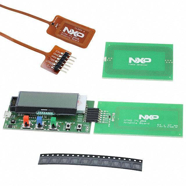
NTAG I²C plus
connected NFC tag
solution by NXP
Your entryway to NFC: The simplest,
most cost-effective NFC solution
Designed to be the perfect enabler for NFC in home-automation and consumer
applications, this feature-packed, next-generation connected NFC tag is the fastest, most
BoM optimized way to add tap-and-go connectivity to just about any electronic device.
KEY FEATURES
`` Interoperability
- NFC interface ISO/IEC 14443A Part 2&3 compliant
- NFC Forum Type 2 Tag compliant
- Input capacitance of 50 pF
- Unique 7-byte serial number
- �GET VERSION command for easy identification of chip type
and supported features
2
`` I C interface
- �Standard (100 kHz) and fast (400 kHz) modes
`` Memory
- 888/1912 bytes of EEPROM-based user memory
- Clear arbitration between NFC and I2C memory access
`` Data transfer
- Pass-through mode with 64-byte SRAM buffer
- �FAST READ and FAST WRITE commands for higher data
throughput
`` Security and memory-access management
- �Full, read-only, or no memory access from NFC interface,
based on 32-bit password protection
- Full, read-only, or no memory access from I2C interface
- �Originality signature based on Elliptic Curve Cryptography
(ECC) for simple, genuine authentication
- �NFC silence to disable the NFC interface
`` Power management
- �Configurable field-detection output signal for data-transfer
synchronization and device wake-up
- �Energy harvesting from NFC field, so as to power external
devices (e.g. connected microcontroller)
KEY BENEFITS
`` Full interoperability with every NFC-enabled device
`` Smooth end-user experience with super-fast data exchange
via NFC and I2C interface
`` Zero-power operation with non-volatile data storage
`` Lowest bill of materials and smallest footprint for NFC
solution in embedded electronics
`` Data protection to prevent unauthorized data manipulation
`` Multi-application support, enabled by memory size and
segmentation options
�APPLICATIONS
`` IoT nodes (home automation, smart home, etc.)
`` Pairing and configuration in consumer applications
`` NFC accessories (headsets, speakers, etc.)
`` Wearable infotainment
`` Fitness equipment
`` Consumer electronics
`` Healthcare
`` Smart printers
`` Meters
`` Electronic shelf labels
NXP NTAG I2C plus is a family of connected NFC tags
that combine a passive NFC interface with a contact I2C
interface. As the second generation of NXP’s industryleading connected-tag technology, these devices maintain
full backward compatibility with first-generation NTAG I2C
products, while adding new, advanced features for password
protection, full memory-access configuration from both interfaces,
and an originality signature for protection against cloning.
The second-generation technology provides four times higher
pass-through performance, along with energy harvesting
capabilities, yet NTAG I2C plus devices are optimized for use in
entry-level NFC applications and offer the lowest BoM of any
NFC solution.
DONE IN AN INSTANT
I2C and NFC communications are based on simple, standard
command sets, and are augmented by the demo board
OM5569/NT322E, which includes online reference source
code. All that’s required is a simple antenna design, with
no or only limited extra components, and there are plenty
of reference designs online for inspiration. The very small
footprint (as low as 1.6 x 1.6 x 0.5 mm) shrinks PCB space and
enables very compact designs.
ZERO POWER BUDGET
NFC tags are passive by default, meaning they can be
powered by another device, to save battery power. Energy
harvesting even lets the tag power an external device, such as
an MCU. The field-detection mechanism enables device wakeup as soon as an NFC field is detected, for longer battery life.
Data storage can be done offline, via non-volatile memory,
from the NFC or I2C interface. Also, since the NFC interface
complies with NFC Forum guidelines, the tag can interact with
a full range of NFC-enabled devices.
BEST USER EXPERIENCE
The integrated SRAM buffer offers faster data transfer than
a standard EEPROM, and is a convenient mechanism for
managing I2C/NFC communication handoffs while keeping
both interfaces active. Fast data transfer is guaranteed by
the pass-through mode, which works with the FAST READ
and FAST WRITE commands to push data in one shot, and
thereby limiting command overhead. The high data-transfer
rates, along with reliable multi-interface communication, create
smoother end-user interactions.
SECURE DATA, CONTROLLED INTERACTIONS
Every type of memory access, including the SRAM buffer,
can be fully configured for both interfaces. For NFC, a 32-bit
password segments the memory into open and restricted
access, to secure data according to specified access rights. For
I2C, access can be restricted to ensure proper data exchange
between embedded electronics and the NFC device. Anticloning protection is supplied by an authentication mechanism
based on a 32-byte, ECC-based signature that uses a standard
algorithm. The result is easy software integration of the
originality check procedure, without the need for specific
hardware requirements.
Feature
Memory
User memory size [bytes]
Write endurance [cycles]
Data retention [years]
Operating temperature [°C]
Storage temperature [°C]
NFC interface
ISO/IEC compliance
NFC Forum compliance
Baudrate [kbits/s]
Resonance capacitance [pF]
I²C interface
Speed [kbit/s]
Supply [V]
Security
Unique serial number [bytes]
Access conditions
Special features
64-byte SRAM buffer
FAST WRITE
FAST READ
ECC-based originality signature
Configurable field detection
Wake-up signal for data-transfer
synchronization
Energy harvesting
Delivery form
Packages
Wafer
NTAG I²C 1k plus
NTAG I²C 2k plus
888
500
20
-40 to +105
-55 to +125
1.912
ISO 14443 A Part 2&3
Type 2 Tag
106
50
100/400
1.67 to 3.6
7
Lock bits / 32-bit password
Yes
Yes
Yes
Yes
Yes
Yes
Yes
XQFN8 / TSSOP8 / SO8
Bumped, 8 inch, 150µm, on film frame carrier
www.nxp.com
© 2015 NXP Semiconductors N.V.
All rights reserved. Reproduction in whole or in part is prohibited without the prior written consent of the copyright owner. The
Date of release: December 2015
information presented in this document does not form part of any quotation or contract, is believed to be accurate and reliable and
Document order number: 9397 750 17701
may be changed without notice. No liability will be accepted by the publisher for any consequence of its use. Publication thereof
Printed in the Netherlands
does not convey nor imply any license under patent- or other industrial or intellectual property rights.
�
