AN11007
Single stage 5-6 GHz WLAN LNA with BFU730F
Rev. 2 — 20 November 2012
Application note
document information
Info
Content
Keywords
BFU730F, LNA, 802.11a & 802.11n MIMO WLAN
Abstract
The document provides circuit, layout, BOM and performance information
on 5-6 GHz band LNA equipped with NXP’s BFU730F wide band
transistor.
This Application note is related to evaluation board
OM7691/BFU730F,598 12nC 934065628598
�AN11007
NXP Semiconductors
5-6 GHz LNA
Revision history
Rev
Date
Description
1
20110104
Initial document.
2
20121120
Chapter added about switching time.
Contact information
For additional information, please visit: http://www.nxp.com
For sales office addresses, please send an email to: salesaddresses@nxp.com
AN11007
Application note
All information provided in this document is subject to legal disclaimers.
Rev. 2 — 20 November 2012
© NXP B.V. 2012. All rights reserved.
2 of 23
�AN11007
NXP Semiconductors
5-6 GHz LNA
1. Introduction
The BFU730F is a discrete HBT that is produced using NXP Semiconductors’ advanced
110 GHz fT SiGe:C BiCmos process. SiGe:C is a normal silicon germanium process with
the addition of Carbon in the base layer of the NPN transistor. The presence of carbon in
the base layer suppresses the boron diffusion during wafer processing. This allows
steeper and narrower SiGe HBT base and a heavier doped base. As a result, lower base
resistance, lower noise and higher cut off frequency can be achieved.
The BFU730F is one of a series of transistors made in SiGe:C.
BFU710F; BFU760 and BFU790 are the other types, BFU710 is intended for ultra low
current applications. The BFU760F and BFU790F are high current types and are
intended for application where linearity is key.
The BFU7XXF are ideal in all kind of applications where cost matters. It also gives
design flexibility.
2. Requirements and design of the 5-6 GHz WLAN LNA
The circuit shown in this application note is intended to demonstrate the performance of
the BFU730 in a 5-6 GHz LNA for e.g. 802.11 & 802.11n “MIMO” WLAN applications.
Key requirements for this application as are:
• NF
• Gain
• Turn on turn of time
• Linearity.
The target for this circuit is listed in table 1.
Table 1.
Target spec.
Target specification of the 5-6GHz LNA.
Vcc
Icc
NF
Gain
IRL
ORL
3
10
15
>10
>10
V
mA
dB
dB
dB
dB
3. Design
The 5-6 GHz LNA consists of one stage BFU730F amplifier. For this amplifier 12 external
components are used, for matching, biasing and decoupling.
The design has been conducted using Agilent’s Advanced Design System (ADS). The
2D EM Momentum tool has been used to co simulate the PCB see Fig 1. Results are
given in paragraph 4.5.
The LNA shows a Gain of 14 dB @5.5 GHz, NF of 1.3 dB, with only 10 mA it shows a
high input P1 dB compression of –7.5 dBm, as well as a input IP3 of +10 dBm.
Finally the LNA is unconditional stable 10 MHz-20 GHz.
AN11007
Application note
All information provided in this document is subject to legal disclaimers.
Rev. 2 — 20 November 2012
© NXP B.V. 2012. All rights reserved.
3 of 23
�AN11007
NXP Semiconductors
5-6 GHz LNA
3.1 BFU730F 5-6 GHz-ADS Simulation circuit
Fig 1.
ADS simulation circuit for 5-6 GHz WLAN LNA
AN11007
Application note
All information provided in this document is subject to legal disclaimers.
Rev. 2 — 20 November 2012
© NXP B.V. 2012. All rights reserved.
4 of 23
�AN11007
NXP Semiconductors
5-6 GHz LNA
3.2 BFU730F 5-6 GHz - ADS Gain and match simulation results
Fig 2.
ADS Gain and match simulation results for 5-6 GHz WLAN LNA
AN11007
Application note
All information provided in this document is subject to legal disclaimers.
Rev. 2 — 20 November 2012
© NXP B.V. 2012. All rights reserved.
5 of 23
�AN11007
NXP Semiconductors
5-6 GHz LNA
3.3 BFU730F 5-6 GHz-ADS NF simulation
Fig 3.
ADS Noise Figure simulation results of 5-6 GHz WLAN LNA
AN11007
Application note
All information provided in this document is subject to legal disclaimers.
Rev. 2 — 20 November 2012
© NXP B.V. 2012. All rights reserved.
6 of 23
�AN11007
NXP Semiconductors
5-6 GHz LNA
3.4 BFU730F 5-6 GHz-ADS Stability simulation
As K≥1 and Mu≥1, the LNA is unconditionally stable for the whole frequency band
Fig 4.
ADS stability simulation results of 5-6 GHz WLAN LNA
AN11007
Application note
All information provided in this document is subject to legal disclaimers.
Rev. 2 — 20 November 2012
© NXP B.V. 2012. All rights reserved.
7 of 23
�AN11007
NXP Semiconductors
5-6 GHz LNA
4. Implementation
4.1 Schematic
R2
R3
C4
GND
Vcc
GND
R1
L3
C3
C5
L2
RF_INPUT
RF_OUTPUT
R4
C2
L4
C6
C1
C7
L1
Fig 5.
5-6 GHz LNA schematic (019aab113)
AN11007
Application note
All information provided in this document is subject to legal disclaimers.
Rev. 2 — 20 November 2012
© NXP B.V. 2012. All rights reserved.
8 of 23
�AN11007
NXP Semiconductors
5-6 GHz LNA
4.2 Layout and assembly
Fig 6.
AN11007
Application note
Layout and assembly info of 5-6 GHz LNA
All information provided in this document is subject to legal disclaimers.
Rev. 2 — 20 November 2012
© NXP B.V. 2012. All rights reserved.
9 of 23
�AN11007
NXP Semiconductors
5-6 GHz LNA
Table 2.
Bill of materials
Designator Description
Size
Q1
2X2 mm
BFU730F
PCB
Value
Type
Note
NXP Semiconductors
HBT
20X35 mm
C1,C7
Capacitor
0402
3.9 pF
MurataGRM1555
input/output
match
C2,C6
Capacitor
0402
0.75 pF
MurataGRM1555
input/output
match
C3
Capacitor
0402
15 nF
MurataGRM1555
C4
Capacitor
0402
1.5 pF
MurataGRM1555
C5
Capacitor
0402
1.5 pF
MurataGRM1555
L1,L4
Inductor
0402
1.5 nH
Murata LQP15
input/output
match
L2
Inductor
0402
9.1 nH
Murata LQW15
input match
L3
Inductor
0402
5.1 nH
Murata LQW15
output match
R1
Resistor
0402
37 K
Bias Setting
R2
Resistor
0402
100 Ohm
Bias Setting
Hfe and
Temp spread
cancellation
R3
Resistor
0402
10 Ohm
Stability
R4
Resistor
0402
0 Ohm
NA
X1,X2
SMA RF
connector
-
Johnson, End launch SMA
142-0701-841
RF input/ RF
output
X3
DC header
-
Molex, PCB header, Right
Angle, 1 row, 3 way 901210763
Bias
connector
4.3 PCB layout.
A good PCB Layout is an essential part of an RF circuit design. The EVB of the BFU730
can serve as a guideline for laying out a board using either the BFU730 or one of the
other SiGe.C HBTs in the SOT343F package. Use controlled impedance lines for all high
frequency inputs and outputs. Bypass VCC with decoupling capacitors, preferable located
as close as possible to the device. For long bias lines it may be necessary to add
decoupling capacitors along the line further away from the device. Proper grounding the
emitters is also essential for the performance. Either connect the emitters directly to the
ground plane ore through vias, or do both.
The material that has been used for the EVB is FR4 using the stack shown in Fig 7.
AN11007
Application note
All information provided in this document is subject to legal disclaimers.
Rev. 2 — 20 November 2012
© NXP B.V. 2012. All rights reserved.
10 of 23
�AN11007
NXP Semiconductors
5-6 GHz LNA
(1) Material supplier is Isola Duraver; Er=4.6-4.9 Tδ=0.02
Fig 7.
PCB material stack
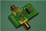
4.4 LNA View
Fig 8.
AN11007
Application note
5-6 GHz LNA EVB
All information provided in this document is subject to legal disclaimers.
Rev. 2 — 20 November 2012
© NXP B.V. 2012. All rights reserved.
11 of 23
�AN11007
NXP Semiconductors
5-6 GHz LNA
4.5 Measurement results
Table 3.
Typical measurement results measured on the evaluation board.
Temp=25 °C, frequency is 5.5 GHz unless otherwise specified.
Parameter
Symbol
Value
Unit
Supply Voltage
Vcc
3
V
Supply Current
Icc
10
mA
Noise Figure
NF
1.3
dB
15.8
dB
14.7
dB
13.7
dB
[1]
5.0 GHz
Power Gain
5.5 GHz
GP
6.0 GHz
Input return Loss
IRL
12
dB
Output return Loss
ORL
13.5
dB
Input 1 dB Gain compression Point
Pi1dB
-7.5
dBm
Output 1 dB Gain compression Point
Po1dB
+6.5
dBm
Input third order intercept point
IP3i
+10
dBm
Output third order intercept point
IP3o
+24
dBm
Ton
160
µs
Toff
28
ns
Remarks
Power settling time
[1]
The NF and Gain figures are being measured at the SMA connectors of the evaluation board, so the
losses of the connectors and the PCB of approximately 0.1dB are not subtracted.
4.5.1 Faster switching time.
很抱歉,暂时无法提供与“OM7691/BFU730F,598”相匹配的价格&库存,您可以联系我们找货
免费人工找货- 国内价格
- 1+1603.40040
- 200+1505.91960