Freescale Semiconductor
Data Sheet: Technical Data
Document Number: P3041EC
Rev. 2, 02/2013
P3041
P3041 QorIQ
Integrated Processor
Hardware Specifications
The P3041 QorIQ integrated processor utilizes four processor
cores built on Power Architecture® technology. The cores
include high-performance data path acceleration logic and
network and peripheral bus interfaces required for
networking, telecom/datacom, wireless infrastructure, and
aerospace applications.
This chip can be used for combined control, data path, and
application layer processing in routers, switches, base station
controllers, and general-purpose embedded computing. Its
high level of integration offers significant performance
benefits compared to multiple discrete devices while also
greatly simplifying board design.
The chip includes the following functions and features:
• Four e500mc Power Architecture cores, each with a
backside 128 KB L2 cache with ECC
– Three levels of instructions: User, supervisor, and
hypervisor
– Independent boot and reset
– Secure boot capability
• CoreNet fabric supporting coherent and non-coherent
transactions amongst CoreNet end-points
• CoreNet platform cache with ECC
• CoreNet bridges between the CoreNet fabric the I/Os,
datapath accelerators, and high and low speed peripheral
interfaces
• One 10-Gigabit Ethernet (XAUI) controller
• Five 1-Gigabit Ethernet controllers
– SGMII interfaces
— 2.5 Gbps SGMII interfaces
– RGMII interfaces
• One 64-bit DDR3 SDRAM memory controller with ECC
• Multicore programmable interrupt controller
• Four I2C controllers
• Four 2-pin UARTs or two 4-pin UARTs
• Two 4-channel DMA engines
© 2010–2013 Freescale Semiconductor, Inc. All rights reserved.
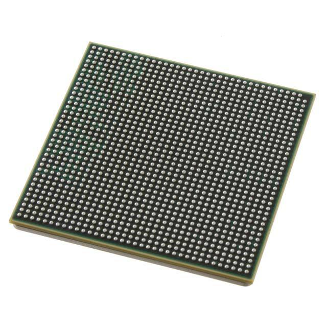
FC-PBGA–1295
37.5 mm x 37.5 mm
• Enhanced local bus controller (eLBC)
• Four PCI Express 2.0 controllers/ports
• Two serial RapidIO® controllers/ports (sRIO port)
supporting version 1.3 with features from 2.1
• Two serial ATA (SATA 2.0) controllers
• Enhanced secure digital host controller (SD/MMC)
• Enhanced serial peripheral interfaces (eSPI)
• 2× high-speed USB 2.0 controllers with integrated PHYs
�Table of Contents
1
2
Pin Assignments and Reset States . . . . . . . . . . . . . . . . . . . . .3
1.1 1295 FC-PBGA Ball Layout Diagrams . . . . . . . . . . . . . .3
1.2 Pinout List . . . . . . . . . . . . . . . . . . . . . . . . . . . . . . . . . . . .9
Electrical Characteristics . . . . . . . . . . . . . . . . . . . . . . . . . . . .51
2.1 Overall DC Electrical Characteristics . . . . . . . . . . . . . .51
2.2 Power-Up Sequencing . . . . . . . . . . . . . . . . . . . . . . . . .56
2.3 Power-Down Requirements . . . . . . . . . . . . . . . . . . . . .58
2.4 Power Characteristics . . . . . . . . . . . . . . . . . . . . . . . . . .59
2.5 Input Clocks . . . . . . . . . . . . . . . . . . . . . . . . . . . . . . . . .62
2.6 RESET Initialization . . . . . . . . . . . . . . . . . . . . . . . . . . .65
2.7 Power-On Ramp Rate . . . . . . . . . . . . . . . . . . . . . . . . . .66
2.8 DDR3 and DDR3L SDRAM Controller . . . . . . . . . . . . .66
2.9 eSPI . . . . . . . . . . . . . . . . . . . . . . . . . . . . . . . . . . . . . . .75
2.10 DUART . . . . . . . . . . . . . . . . . . . . . . . . . . . . . . . . . . . . .77
2.11 Ethernet: Datapath Three-Speed Ethernet (dTSEC),
Management Interface, IEEE Std 1588. . . . . . . . . . . . .78
2.12 USB. . . . . . . . . . . . . . . . . . . . . . . . . . . . . . . . . . . . . . . .86
2.13 Enhanced Local Bus Interface (eLBC) . . . . . . . . . . . . .87
2.14 Enhanced Secure Digital Host Controller (eSDHC) . . .91
2.15 Multicore Programmable Interrupt Controller (MPIC) and
Trust Specifications . . . . . . . . . . . . . . . . . . . . . . . . . . . .93
2.16 JTAG Controller. . . . . . . . . . . . . . . . . . . . . . . . . . . . . . .94
3
4
5
6
7
2.17 I2C . . . . . . . . . . . . . . . . . . . . . . . . . . . . . . . . . . . . . . . . 96
2.18 GPIO . . . . . . . . . . . . . . . . . . . . . . . . . . . . . . . . . . . . . . 99
2.19 High-Speed Serial Interfaces (HSSI) . . . . . . . . . . . . . 100
Hardware Design Considerations . . . . . . . . . . . . . . . . . . . . 132
3.1 System Clocking . . . . . . . . . . . . . . . . . . . . . . . . . . . . 132
3.2 Supply Power Default Setting . . . . . . . . . . . . . . . . . . 139
3.3 Power Supply Design . . . . . . . . . . . . . . . . . . . . . . . . 141
3.4 Decoupling Recommendations . . . . . . . . . . . . . . . . . 143
3.5 SerDes
Block
Power
Supply
Decoupling
Recommendations. . . . . . . . . . . . . . . . . . . . . . . . . . . 143
3.6 Connection Recommendations . . . . . . . . . . . . . . . . . 143
3.7 Recommended Thermal Model . . . . . . . . . . . . . . . . . 152
3.8 Thermal Management Information . . . . . . . . . . . . . . 153
Package Information . . . . . . . . . . . . . . . . . . . . . . . . . . . . . . 154
4.1 Package Parameters for the FC-PBGA . . . . . . . . . . . 154
4.2 Mechanical Dimensions of the FC-PBGA . . . . . . . . . 155
Security Fuse Processor . . . . . . . . . . . . . . . . . . . . . . . . . . . 156
Ordering Information . . . . . . . . . . . . . . . . . . . . . . . . . . . . . . 156
6.1 Part Numbering Nomenclature . . . . . . . . . . . . . . . . . 156
6.2 Orderable Part Numbers Addressed by this Document157
Revision history . . . . . . . . . . . . . . . . . . . . . . . . . . . . . . . . . . 158
P3041 QorIQ Integrated Processor Hardware Specifications, Rev. 2
2
Freescale Semiconductor
�Pin Assignments and Reset States
This figure shows the major functional units within the chip.
P3041
128-Kbyte
Backside
L2 Cache
Power Architecture®
e500mc Core
32-Kbyte
D-Cache
1024-Kbyte
Frontside
CoreNet Platform
Cache
32-Kbyte
I-Cache
eOpenPIC
PreBoot
Loader
64-bit
DDR3/3L
Memory Controller
CoreNet
Coherency Fabric
Security
Monitor
PAMU
PAMU
Peripheral
PAMU Access Mgmt Unit
PAMU
Internal
BootROM
Power Mgmt
PAMU
Frame Manager
Security
4.2
Queue
Mgr
Parse, Classify,
Distribute
2x DMA
1GE
10GE
1GE
1GE
1GE
Clocks/Reset
1GE
PCIe 2.0
Buffer
Mgr
PCIe 2.0
Pattern
Match
Engine
2.1
sRIO 1.3/2.1
RapidIO
RMan
sRIO 1.3/2.1
2x
USB 2.0 PHY
PCIe
4x I2C
PCIe 2.0
Buffer
2x DUART
SATA 2.0
eLBC
SPI
Real Time Debug
SATA 2.0
SD/MMC
Watchpoint
Cross
Trigger
Perf CoreNet
Monitor Trace
Aurora
GPIO
18-Lane 5-GHz SerDes
CCSR
Figure 1. Block Diagram
1
Pin Assignments and Reset States
This section contains top view and detailed quadrant views of the FC-PBGA ball map diagram followed by a pinout list.
1.1
1295 FC-PBGA Ball Layout Diagrams
These figures show the FC-PBGA ball map diagrams.
P3041 QorIQ Integrated Processor Hardware Specifications, Rev. 2
Freescale Semiconductor
3
�Pin Assignments and Reset States
1
A
2
3
4
5
6
7
8
9
10
11
12
13
14
15
16
17
18
19
20
21
22
23
24
25
26
27
28
29
30
31
32
33
34
RSRV
[A2]
RSRV
[A3]
RSRV
[A4]
RSRV
[A5]
RSRV
[A6]
RSRV
[A7]
RSRV
[A8]
RSRV
[A9]
RSRV
[A10]
RSRV
[A11]
RSRV
[A12]
RSRV
[A13]
MDQ
[3]
MDQ
[6]
MDM
[0]
MDQ
[0]
GND
[24]
AVDD_
DDR
AVDD_
CC
[1]
RSRV
[A21]
GND
[21]
LALE
LWE
[1]
RSRV
[A25]
GND
[23]
NC
[A27]
SGND
[1]
SD_RX
[1]
SVDD
[1]
SD_RX
[3]
SGND
[2]
AVDD_
SRDS1
SVDD
[2]
GND
[17]
LCS
[5]
BVDD
[1]
LGPL
[0]
NC
[B26]
SD_IMP_ SVDD
CAL_RX
[9]
SD_RX
[1]
SGND
[10]
SD_RX
[3]
SVDD
[10]
AGND_
SRDS1
SGND
[11]
LCLK
[1]
LCLK
[0]
LGPL
[4]
NC
[C26]
NC
[C27]
SD_RX
[0]
SGND
[12]
SD_RX
[2]
SVDD
[12]
RSRV
[C32]
SGND
[13]
SVDD
[13]
35
SD_
REF_
CLK1
SD_
REF_
CLK1
36
SGND
[3]
A
SVDD
[11]
B
SVDD
[14]
SD_RX
[4]
C
B
RSRV
[B1]
GVDD
[1]
RSRV
[B3]
RSRV
[B4]
GND
[2]
RSRV
[B6]
RSRV
[B7]
GVDD
[2]
RSRV
[B9]
RSRV
[B10]
GND
[7]
RSRV
[B12]
RSRV
[B13]
GVDD
[3]
MDQ
[7]
MDQS
[0]
MDQ
[5]
GND
[31]
MVREF
GND
[16]
TEMP_
CATHODE
C
RSRV
[C1]
RSRV
[C2]
GND
[1]
RSRV
[C4]
RSRV
[C5]
GVDD
[6]
RSRV
[C7]
MDQ
[16]
GND
[6]
MDQ
[21]
MDQ
[20]
GVDD
[5]
RSRV
[C13]
MDQ
[2]
GND
[14]
MDQS
[0]
MDQ
[4]
GVDD
[4]
NC
[C19]
NC
[C20]
TEMP_
LBCTL
ANODE
D
RSRV
[D1]
RSRV
[D2]
RSRV
[D3]
GVDD
[7]
RSRV
[D5]
RSRV
[D6]
GND
[5]
MDQS
[2]
MDQS
[2]
GVDD
[8]
MDM
[2]
MDQ
[17]
GND
[13]
MDM
[1]
MDQ
[8]
GVDD
[9]
MDQ
[1]
NC
[D18]
LCS
[0]
LCS
[1]
LCS
[3]
LCS
[4]
LAD
[9]
LWE
[0]
LGPL
[2]
LAD
[27]
NC
[D27]
SD_RX
[0]
SVDD
[15]
SD_RX
[2]
SGND
[14]
RSRV
[D32]
XGND
[9]
SD_TX
[4]
SGND
[15]
SD_RX
[4]
D
E
RSRV
[E1]
GVDD
[12]
RSRV
[E3]
RSRV
[E4]
GND
[4]
MDQ
[22]
MDQ
[23]
GVDD
[11]
MDQ
[18]
MDQ
[19]
GND
[12]
MDQ
[10]
MDQ
[14]
GVDD
[10]
MDQ
[13]
NC
[E16]
GND
[25]
LA
[28]
GND
[18]
LCS
[2]
LAD
[21]
BVDD
[6]
LAD
[8]
BVDD
[5]
LGPL
[1]
LGPL
[5]
NC
[E27]
XGND
[10]
SD_TX
[1]
XGND
[11]
SD_TX
[3]
XVDD
[8]
XVDD
[9]
SD_TX
[4]
SGND
[16]
SVDD
[16]
E
F
RSRV
[F1]
RSRV
[F2]
GND
[3]
RSRV
[F4]
RSRV
[F5]
GVDD
[13]
MDQ
[24]
MDQ
[29]
GND
[11]
MDQ
[28]
MDQ
[25]
GVDD
[14]
MDQ
[15]
MDQS
[1]
GND
[36]
MDQ
[12]
LAD
[31]
LA
[29]
LAD
[12]
BVDD
[3]
LAD
[22]
LAD
[19]
GND
[26]
LCS
[6]
LAD
[4]
BVDD
[4]
GND
[28]
XVDD
[10]
SD_TX
[1]
XVDD
[11]
SD_TX
[3]
XGND
[12]
SD_TX
[5]
SVDD
[17]
SD_RX SD_RX
[5]
[5]
F
G
RSRV
[G1]
RSRV
[G2]
RSRV
[G3]
GVDD
[16]
RSRV
[G5]
RSRV
[G6]
GND
[10]
MDQS
[3]
MDQS
[3]
GVDD
[17]
MDM
[3]
MDQ
[11]
GND
[35]
MDQS
[1]
MDQ
[9]
GVDD
[18]
GND
[231]
LA
[31]
LAD
[28]
LAD
[25]
GND
[29]
LAD
[11]
LAD
[7]
LAD
[6]
LAD
[17]
LCS
[7]
NC
[G27]
SD_TX
[0]
XGND
[13]
SD_TX
[2]
XGND
[14]
XVDD
[12]
SD_TX
[5]
SGND
[17]
SVDD
[18]
SGND
[18]
G
H
RSRV
[H1]
GVDD
[21]
RSRV
[H3]
RSRV
[H4]
GND
[9]
RSRV
[H6]
MDQ
[30]
GVDD
[20]
MDQ
[31]
MDQ
[26]
GND
[37]
NC
[H12]
NC
[H13]
GVDD
[19]
NC
[H15]
LDP
[3]
LDP
[2]
BVDD
[9]
LAD
[29]
BVDD
[8]
LAD
[23]
LAD
[20]
LAD
[18]
LAD
[5]
LAD
[3]
LGPL
[3]
NC
[H27]
SD_TX
[0]
XGND
[15]
SD_TX
[2]
XVDD
[13]
XGND
[16]
XVDD
[14]
XGND
[17]
SD_RX SD_RX
[6]
[6]
H
J
RSRV
[J1]
RSRV
[J2]
GND
[8]
RSRV
[J4]
MECC
[1]
GVDD
[22]
MECC
[5]
MECC
[4]
GND
[38]
MDQ
[27]
NC
[J11]
GVDD
[25]
NC
[J13]
NC
[J14]
LAD
[30]
LWE
[2]
LAD
[15]
LAD
[13]
LAD
[30]
LAD
[26]
GND
[33]
LAD
[10]
GND
[20]
LDP
[0]
LAD
[16]
LAD
[2]
GND
[27]
XVDD
[15]
XGND
[18]
XVDD
[16]
XGND
[19]
XVDD
[17]
SD_TX
[6]
SD_TX
[6]
SGND
[19]
SVDD
[19]
J
K
RSRV
[K1]
RSRV
[K2]
RSRV
[K3]
GVDD
[24]
MDQS
[8]
MDQS
[8]
GND
[39]
MDM
[8]
MECC
[0]
GVDD
[23]
NC
[K11]
NC
[K12]
NC
[K13]
NC
[K14]
LAD
[14]
GND
[15]
LAD
[27]
LAD
[24]
BVDD
[2]
LDP
[1]
BVDD
[7]
GND
[30]
LAD
[0]
RSRV
[K27]
XGND
[20]
XGND
[21]
XVDD
[18]
SD_TX
[7]
SD_TX
[7]
SGND
[20]
SVDD
[20]
SD_RX SD_RX
[7]
[7]
K
L
RSRV
[L1]
GVDD
[25]
RSRV
[L3]
RSRV
[L4]
GND
[40]
MA
[15]
MECC
[6]
GVDD
[26]
MECC
[7]
VDD
MECC
_CA_PL
[2]
[1]
GND
[230]
VDD
_CA_PL
[2]
GND
[141]
GND
[32]
VDD
_CA_PL
[5]
GND
[22]
VDD
_CA_PL
[6]
GND
[19]
VDD
_CA_PL
[7]
GND
[209]
VDD
_CA_PL
[8]
LAD
[1]
RSRV
[L27]
RSRV
[L28]
XGND
[22]
XVDD
[19]
XVDD
[20]
XGND
[23]
SD_RX SD_RX
[8]
[8]
SVDD
[21]
L
M
RSRV
[M1]
RSRV
[M2]
GND
[41]
RSRV
[M4]
RSRV
[M5]
GVDD
[27]
MA
[14]
MBA
[2]
GND
[45]
MECC
[3]
GND
[113]
VDD
_CA_PL
[9]
GND
[127]
VDD
_CA_PL
[10]
GND
[142]
VDD
_CA_PL
[11]
GND
[157]
VDD
_CA_PL
[12]
GND
[178]
VDD
_CA_PL
[13]
GND
[193]
VDD
_CA_PL
[14]
GND
[208]
VDD
_CA_PL
[15]
GND
[225]
VDD
_CA_PL
[16]
GND
[34]
RSRV
[M28]
XVDD
[21]
XGND
[24]
SD_TX
[8]
SD_TX
[8]
SVDD
[22]
SGND
[22]
SD_RX SD_RX
[9]
[9]
M
N
RSRV
[N1]
RSRV
[N2]
RSRV
[N3]
GVDD
[28]
RSRV
[N5]
MA
[12]
GND
[44]
MAPAR_ MCKE
[3]
ERR
GVDD
[29]
VDD
_CA_PL
[17]
GND
[126]
VDD
_CA_PL
[19]
GND
[N14]
VDD
_CA_PL
[19]
GND
[156]
VDD
_CA_PL
[20]
GND
160]
VDD
_CA_PL
[21]
GND
[179]
VDD
_CA_PL
[22]
GND
[200]
VDD
_CA_PL
[23]
GND
[210]
VDD
_CA_PL
[24]
GND
[112]
VDD
_CA_PL
[25]
RSRV
[N28]
XGND
[25]
XGND
[26]
XVDD
[22]
XGND
[27]
SD_TX
[9]
SD_TX
[9]
SGND
[23]
SVDD
[23]
N
P
RSRV
[P1]
GVDD
[31]
RSRV
[P3]
RSRV
[P4]
GND
[43]
MA
[9]
MA
[11]
GVDD
[30]
MCKE
[2]
MCKE
[0]
GND
[113]
VDD
_CA_PL
[26]
GND
[128]
VDD
_CA_PL
[27]
GND
[P15]
VDD
_CA_PL
[28]
GND
[P17]
VDD
_CA_PL
[29]
GND
[177]
VDD
_CA_PL
[30]
GND
[192]
VDD
_CA_PL
[31]
GND
[207]
VDD
_CA_PL
[32]
GND
[224]
VDD
_CA_PL
[33]
GND
[221]
RSRV
[P28]
XGND
[28]
XVDD
[23]
SD_TX
[10]
SD_TX
[10]
XVDD
[24]
XGND
[29]
SD_RX SD_RX
[10]
[10]
P
R
RSRV
[R1]
RSRV
[R2]
GND
[42]
RSRV
[R4]
RSRV
[R5]
GVDD
[32]
MA
[8]
MA
[7]
GND
[47]
VDD
MCKE
_CA_PL
[1]
[34]
GND
[125]
VDD
_CA_PL
[35]
GND
[139]
VDD
_CA_PL
[36]
GND
[155]
VDD
_CA_PL
[37]
GND
[161]
VDD
_CA_PL
[38]
GND
[180]
VDD
_CA_PL
[39]
GND
[199]
VDD
_CA_PL
[40]
GND
[211]
VDD
_CA_PL
[41]
GND
[111]
VDD
_CA_PL
[42]
NC
[R28]
XVDD
[25]
XGND
[30]
XVDD
[26]
XGND
[31]
SGND
[24]
SVDD
[24]
SVDD
[25]
SGND
[25]
R
T
RSRV
[T1]
RSRV
[T2]
RSRV
[T3]
GVDD
[34]
RSRV
[T5]
MDIC
[0]
GND
[48]
MA
[5]
MA
[6]
GVDD
[33]
GND
[115]
VDD
_CA_PL
[43]
GND
[129]
VDD
_CA_PL
[44]
GND
[144]
VDD
_CA_PL
[45]
GND
[159]
VDD
_CA_PL
[46]
GND
[176]
VDD
_CA_PL
[47]
GND
[191]
VDD
_CA_PL
[48]
GND
[206]
VDD
_CA_PL
[49]
GND
[223]
VDD
_CA_PL
[50]
GND
[226]
NC
[T28]
XVDD
[27]
SD_TX
[11]
SD_TX
[11]
XVDD
[28]
SD_RX
[11]
SD_RX
[11]
SGND
[26]
AGND_
SRDS2
T
U
RSRV
[U1]
GVDD
[36]
GND
[50]
RSRV
[U4]
GND
[49]
MA
[1]
MA
[2]
GVDD
[37]
MA
[3]
MA
[4]
VDD
_CA_PL
[51]
GND
[124]
VDD
_CA_PL
[52]
GND
[138]
VDD
_CA_PL
[53]
GND
[154]
VDD
_CA_PL
[54]
GND
[162]
VDD
_CA_PL
[55]
GND
[181]
VDD
_CA_PL
[56]
GND
[198]
VDD
_CA_PL
[57]
GND
[212]
VDD
_CA_PL
[58]
GND
[110]
VDD
_CA_PL
[59]
NC
[U28]
XGND
[32]
XVDD
[29]
XGND
[33]
RSVD
[U32]
SVDD
[26]
SGND
[27]
AVDD_
SRDS2
U
V
RSRV
[V1]
RSRV
[V2]
RSRV
[V3]
RSRV
[V4]
MCK
[1]
MCK
[1]
GVDD
[38]
MCK
[2]
MCK
[2]
GND
[54]
GND
[116]
VDD
_CA_PL
[60]
GND
[130]
VDD
_CA_PL
[61]
GND
[145]
VDD
_CA_PL
[62]
GND
[222]
VDD
_CA_PL
[63]
GND
[175]
VDD
_CA_PL
[64]
GND
[190]
VDD
_CA_PL
[65]
GND
[205]
VDD
_CA_PL
[66]
GND
[46]
VDD
_CA_PL
[67]
GND
[227]
NC
[V28]
XGND
[34]
XVDD
[30]
XGND
[35]
XVDD
[31]
SD_
REF_
CLK2
SD_
REF_
CLK2
SVDD
[27]
SGND
[28]
V
W
RSRV
[W1]
RSRV
[W2]
RSRV
[W3]
RSRV
[W4]
MCK
[0]
MCK
[0]
GND
[53]
MCK
[3]
MCK
[3]
VDD
GVDD
_CA_PL
[40]
[68]
GND
[123]
VDD
_CA_PL
[69]
GND
[137]
VDD_CB
[1]
GND
[150]
VDD_CB
[12]
GND
[167]
VDD_CB
[2]
GND
[185]
VDD
_CA_PL
[70]
GND
[197]
VDD
_CA_PL
[71]
GND
[213]
VDD
_CA_PL
[72]
GND
[109]
NC_
W27_
DET
VDD
_CA_PL
[1]
XVDD
[32]
XGND
[36]
SD_TX
[12]
SD_TX
[12]
SGND
[29]
SVDD
[28]
SD_RX SD_RX
[12]
[12]
Y
RSRV
[Y1]
GVDD
[43]
GND
[51]
RSRV
[Y4]
GND
[52]
RSRV MAPAR_ GVDD
[Y6]
OUT
[44]
GND
[117]
VDD
_CA_PL
[73]
GND
[131]
VDD
_CA_PL
[74]
GND
[146]
VDD_CB
[7]
GND
[163]
VDD_CB
[13]
GND
[174]
VDD_CB
[4]
GND
[189]
VDD
_CA_PL
[75]
GND
[204]
VDD
_CA_PL
[76]
GND
[220]
VDD
_CA_PL
[77]
GND
[228]
NC
[Y28]
SD_TX
[13]
SD_TX
[13]
XVDD
[33]
XGND
[37]
SD_RX
[13]
SD_RX
[13]
SGND
[30]
AA
RSRV
[AA1]
RSRV
[AA2]
RSRV
[AA3]
RSRV
[AA4]
MDIC
[1]
GVDD
[41]
MA
[10]
AB
RSRV
[AB1]
RSRV
[AB2]
RSRV
[AB3]
GVDD
[51]
MDQ
[36]
MDQ
[37]
AC
RSRV
[AC1]
GVDD
[45]
RSRV
[AC3]
RSRV
[AC4]
GND
[57]
AD
RSRV
[AD1]
RSRV
[AD2]
GND
[58]
MDQS
[4]
AE
RSRV
[AE1]
RSRV
[AE2]
RSRV
[AE3]
AF
RSRV
[AF1]
GVDD
[49]
AG
RSRV
[AG1]
AH
SEE DETAIL A
SENSE- SENSEVDD_CA GND_CA
_PL
_PL
VDD
VDD
_CA_PL GND _CA_PL
[98]
[3]
[4]
LWE
[3]
SEE DETAIL B
RSVD
[U35]
SGND
[21]
SVDD
[29]
W
MA
[0]
MBA
[1]
MBA
[0]
GND
[55]
MRAS
VDD
_CA_PL
[78]
GND
[122]
VDD
_CA_PL
[79]
GND
[136]
VDD_CB
[8]
GND
[152]
VDD_CB
[10]
GND
[169]
VDD_CB
[3]
GND
[183]
VDD_CB
[6]
GND
[196]
VDD
_CA_PL
[80]
GND
[214]
VDD
_CA_PL
[81]
GND
[108]
VDD
_CA_PL
[82]
NC
[AA28]
XVDD
[1]
XGND
[1]
SD_TX
[14]
SD_TX
[14]
SVDD
[3]
SGND
[4]
SD_RX SD_RX
[14]
[14]
AA
GND
[56]
MWE
MCS
[2]
GVDD
[52]
GND
[118]
VDD
_CA_PL
[83]
GND
[132]
VDD_CB
[5]
GND
[147]
VDD_CB
[15]
GND
[164]
VDD_CB
[14]
GND
[173]
VDD_CB
[17]
GND
[188]
VDD
_CA_PL
[84]
GND
[203]
VDD
_CA_PL
[85]
GND
[219]
VDD
_CA_PL
[86]
GND
[87]
NC
[AB28]
NC
[AB29]
XVDD
[2]
XVDD
[3]
XGND
[2]
SD_TX
[15]
SD_TX
[15]
SVDD
[4]
SGND
[5]
AB
MDQ
[33]
MDQ
[32]
GVDD
[53]
MCS
[0]
MCAS
VDD
_CA_PL
[87]
GND
[121]
VDD
_CA_PL
[88]
GND
[135]
VDD_CB
[9]
GND
[151]
VDD_CB
[11]
GND
[168]
VDD_CB
[16]
GND
[184]
VDD
_CA_PL
[89]
GND
[195]
VDD
_CA_PL
[90]
GND
[215]
VDD
_CA_PL
[91]
GND
[107]
VDD
_CA_PL
[92]
NC_
AC28
NC
[AC29]
XGND
[3]
SD_
REF_
CLK3
SD_
REF_
CLK3
XVDD
[4]
XGND
[4]
SD_RX SD_RX
[15]
[15]
AC
MDQS
[4]
GVDD
[46]
MDM
[4]
MODT
[2]
GND
[59]
MODT
[0]
GND
[119]
VDD
_CA_PL
[93]
GND
[133]
VDD
_CA_PL
[94]
GND
[148]
VDD
_CA_PL
[95]
GND
[165]
VDD
_CA_PL
[96]
GND
[172]
VDD
_CA_PL
[97]
GND
[187]
VDD
_CA_PL
[98]
GND
[202]
VDD
_CA_PL
[99]
GND
[218]
VDD
_CA_PL
[100]
GND
[229]
VDD_
LP
NC
[AD29]
XGND
[5]
XGND
[6]
XVDD
[5]
RSVR
[AD33]
RSVR
[AD34]
SGND
[6]
SVDD
[5]
AD
GVDD
[48]
MDQ
[38]
MDQ
[39]
GND
[60]
MA
[13]
MCS
[1]
VDD
GVDD
_CA_PL
[47]
[101]
GND
[120]
VDD
_CA_PL
[102]
GND
[134]
VDD
_CA_PL
[103]
GND
[153]
VDD
_CA_PL
[104]
GND
[170]
VDD
_CA_PL
[105]
GND
[182]
VDD
_CA_PL
[106]
GND
[194]
VDD
_CA_PL
[107]
GND
[216]
VDD
_CA_PL
[108]
GND
[106]
GND
[97]
NC
LP_TMP
_DETECT [AE29]
XVDD
[6]
SD_TX
[16]
SD_TX
[16]
SVDD
[6]
SGND
[7]
AVDD_ AGND_
SRDS3 SRDS3
AE
RSRV
[AF3]
RSRV
[AF4]
GND
[61]
MDQ
[34]
MDQ
[35]
GVDD
[50]
MCS
[3]
MODT
[3]
RSRV
[AF11]
RSRV
[AF12]
GND
[85]
VDD
_CA_PL
[109]
GND
[149]
VDD
_CA_PL
[110]
GND
[166]
VDD
_CA_PL
[111]
GND
[171]
VDD
_CA_PL
[112]
GND
[186]
VDD
_CA_PL
[113]
GND
[201]
VDD
_CA_PL
[114]
GND
[217]
NC
[AF26]
NC
[AF27]
NC
[AF28]
NC
SD_IMP_ XVDD
[AF29] CAL_TX
[7]
XGND
[7]
SD_RX
[16]
SD_RX
[16]
SVDD
[7]
SGND
[8]
AF
RSRV
[AG2]
GND
[62]
RSRV
[AG4]
MDQ
[40]
GVDD
[54]
MDQ
[45]
MDQ
[44]
GND
[63]
MODT
[1]
RSRV_
AG12
RSRV_
AG12
IRQ
[8]
IIC4_
SCL
SENSE- SENSEVDD_CB GND_CB
IRQ
[6]
SDHC
_DAT[3]
SDHC
_CMD
CVDD
[3]
RSRV
[AG25]
NC
[AG26]
NC
[AG27]
NC
[AG28]
NC
[AG29]
XGND
[8]
SD_TX
[17]
SD_TX
[17]
SGND
[9]
SVDD
[8]
SD_RX SD_RX
[17]
[17]
AG
RSRV
[AH1]
RSRV
[AH2]
RSRV
[AH3]
GVDD
[56]
MDQS
[5]
MDQS
[5]
GND
[64]
MDM
[5]
MDQ
[41]
GVDD
[55]
RSRV
AH11
GND
[72]
IRQ
[10]
IIC1_
SCL
IRQ
[1]
IRQ
[4]
DMA2_ GPIO
OVDD
DACK
[7]
[7]
[0]
IO_
MSRCID VSEL MSRCID GPIO
[0]
[4]
[2]
[4]
UART2_ USB1_
AGND
CTS
USB1_
VDD_
1P0
USB2_
VDD_
1P0
USB2_
TMS
AGND
SPI_
MISO
RSRV
[AH29]
NC
[AH30]
XGND
[38]
XVDD
[34]
SGND
[32]
GND
[102]
SGND
[31]
SVDD
[30]
AH
AJ
RSRV
[AJ1]
GVDD
[57]
RSRV
[AJ3]
RSRV
[AJ4]
GND
[65]
MDQ
[46]
MDQ
[47]
GVDD
[58]
MDQ
[42]
MDQ
[43]
GND
[71]
OVDD
[5]
IRQ
[5]
OVDD
[2]
IRQ
[3]
IRQ
[0]
EVT
[0]
USB2_
VDD_
3P3
USB2_ SPI_CS
VDD_
[1]
3P3
CVDD
[1]
EMI2_ EC_XTRNL
MDIO _TX_STMP
[2]
GND
[100]
TSEC_
TSEC_
LV
EMI1_
1588_PULSE DD 1588_ALARM
MDC
[5]
_OUT[1]
_OUT[2]
AK
RSRV
[AK1]
RSRV
[AK2]
GND
[66]
RSRV
[AK4]
RSRV
[AK5]
GVDD
[60]
MDQ
[53]
MDQ
[52]
GND
[70]
GVDD
[39]
IRQ
[9]
IRQ
[2]
IIC3_
SCL
IRQ_
OUT
GND
[78]
EVT
[3]
EVT
[1]
USB1_
VDD_
3P3
USB1_
VBUS_
CLMP
AL
RSRV
[AL1]
RSRV
[AL2]
RSRV
[AL3]
GVDD
[61]
RSRV
[AL5]
RSRV
[AL6]
GND
[69]
MDQ
[49]
MDQ
[48]
GVDD
[62]
MDM
[6]
IRQ
[11]
GND
[77]
IIC2_
SDA
IIC4_
SDA
OVDD
[4]
SCAN_
MODE
AM
RSRV
[AM1]
GVDD
[63]
RSRV
[AM3]
RSRV
[AM4]
GND
[68]
RSRV
[AM6]
RSRV
[AM7]
GVDD
[64]
MDQS
[6]
MDQS
[6]
GND
[76]
NC
[AM12]
IRQ
[7]
IIC3_
SDA
IIC2_
SCL
EVT
[4]
GND
[83]
AN
RSRV
[AN1]
RSRV
[AN2]
GND
[67]
RSRV
[AN4]
RSRV
[AN5]
GVDD
[67]
MDQ
[54]
MDQ
[55]
GND
[75]
MDQ
[50]
MDQ
[51]
GVDD
[66]
NC
[AN13]
IIC1_
SDA
GND
[82]
EVT
[2]
TDI
AP
RSRV
[AP1]
RSRV
[AP2]
RSRV
[AP3]
GVDD
[68]
RSRV
[AP5]
RSRV
[AP6]
GND
[74]
RSRV
[AP8]
MDQ
[60]
GVDD
[65]
NC
[AP11]
MDQ
[63]
GND
[81]
NC
[AP14]
TDO
AR
RSRV
[AR1]
GVDD
[42]
RSRV
[AR3]
RSRV
[AR4]
GND
[73]
RSRV
[AR6]
RSRV
[AR7]
GVDD
[15]
MDQ
[61]
MDQ
[57]
GND
[80]
MDQ
[62]
MDQ
[59]
GVDD
[59]
MDVAL
AT
RSRV
[AT1]
RSRV
[AT2]
RSRV
[AT3]
RSRV
[AT4]
RSRV
[AT5]
RSRV
[AT6]
RSRV
[AT7]
RSRV
[AT8]
MDQ
[56]
MDM
[7]
MDQS
[7]
MDQS
[7]
MDQ
[58]
NC
[AT14]
OVDD RESET_
AVDD_
POVDD
CC2
[9]
REQ
1
2
3
4
5
6
7
8
9
10
11
12
13
14
SEE DETAIL C
RSRV_
AH12
15
GND
[79]
OVDD MSRCID DMA2_
DREQ
[3]
[1]
[0]
IO_
CLK_
GND
VSEL
[84]
OUT
[2]
16
HRESET
17
GPIO
[5]
UART2_
SOUT
GPIO
[6]
GPIO
[1]
OVDD
[10]
SEE DETAIL D
USB1_
AGND
TSEC_
EC1_ TSEC_
EMI2_ EC_XTRNL EC_XTRNL LVDD
GTX_ 1588_ALARM1588_TRIG
[1]
MDC _RX_STMP _RX_STMP
_IN[2]
CLK125 _OUT[2]
[2]
[1]
TSEC_
EC2_
TSEC_
TSEC_
LV
EMI1_
GND
GND
1588_PULSE DD
GTX_
[104] 1588_CLK 1588_TRIG
[91]
MDIO
[3]
_OUT[1]
CLK125
_IN[1]
_IN
EC1_
LVDD
EC1_
EC1_
USB2_ SPI_CS TSEC_ EC_XTRNL GND
RXD
_TX_STMP [105]
RX_CLK
RX_DV
AGND
[7]
[3] 1588_CLK_
[3]
[1]
OUT
EC2_
EC1_
EC1_
EC1_
EC2_
LVDD
USB2_ SPI_CS GND
RXD
RXD
RXD
GTX_CLK RXD
AGND
[101]
[4]
[0]
[2]
[1]
[0]
[2]
OVDD
[8]
GPIO
[0]
UART1_ SHDC_
SOUT
CLK
USB1_
VDD_
3P3
USB2_ USB2_
GND
VBUS_
UID
[96]
CLMP
USB2_
USB1_
USB1_
USB2_
VDD_1P8 VDD_1P8
AGND
AGND
_DECAP _DECAP
IO_
CKSTP_
VSEL
OUT
[3]
GPIO
[2]
GND
[90]
UART1_ SDHC_
DAT
RTS
[2]
USB_
CLKIN
USB1_
AGND
USB1_
IBIAS_
REXT
USB2_
IBIAS_
REXT
OVDD TMP_
DETECT
[6]
GPIO
[3]
DMA1_
DDONE
[0]
OVDD UART2_
[1]
SIN
RTC
USB2_
AGND
USB2_
AGND
USB2_
AGND
DMA2_
DDONE
[0]
DMA1_
DREQ
[0]
USB2_
UDP
IO_
VSEL
[0]
IO_
OVDD
PORESET VSEL
[11]
[1]
GND
[92]
GND
[89]
GND
[86]
18
DMA1_
DACK
[0]
GND
[88]
UART2_ USB1_
UID
RTS
UART1_
CTS
GND
[94]
SDHC
_DAT
[0]
USB2_
AGND
USB2_
UDM
OVDD
[12]
USB1_
AGND
USB1_ USB1_
AGND AGND
TRST
TMS
ASLEEP
TCK
UART1_
SIN
RSRV
[AT19]
AVDD_
PLAT
TEST
SEL_
GND
[93]
SYSCLK
SDHC
_DAT
[1]
USB1_
AGND
USB1_
UDM
19
20
21
22
23
24
25
26
USB2_
AGND
SPI_
CLK
CVDD
[2]
USB1_ SPI_CS
AGND
[2]
USB1_ USB1_
AGND
UDP
27
28
EC2_
TXD
[2]
EC2_
TXD
[1]
Y
AJ
AK
AL
AM
AN
LVDD
[2]
EC2_
RXD
[1]
EC2_
RXD
[3]
GND
[99]
EC1_
GTX_
CLK
EC1_
TXD
[3]
AP
EC2_
TX_EN
GND
[95]
EC2_
RX_
DV
EC1_
TXD
[1]
LVDD
[6]
EC1_
TX_EN
AR
AT
SPI_
MOSI
EC2_
TXD
[0]
EC2_
TXD
[3]
EC2_
RXD
[0]
EC2_
RX_
CLK
EC1_
TXD
[2]
EC1_
TXD
[0]
GND
[103]
29
30
31
32
33
34
35
36
Signal Groups
OVDD
I/O Supply Voltage
SVDD
SerDes Core Power Supply
AVDD_
SRDS1
SerDes 1 PLL Supply Voltage
SENSEVDD
Core Group A Voltage Sense
LVDD
I/O Supply Voltage
XVDD
SerDes Transcvr Pad Supply
AVDD_
SRDS2
SerDes 2 PLL Supply Voltage
SENSEVDD_CB
Core Group B Voltage Sense
GVDD
DDR DRAM I/O Supply
Core A, B and Platform Supply
Voltage
AVDD_
PLAT
Platform PLL Supply Voltage
CVDD
SPI Voltage Supply
Core Group B Supply Voltage
AVDD_
CC
Core PLL Supply Voltage
BVDD
Local Bus I/O Supply
VDD_
CA_CB_PL
VDD_
CB
POVDD
SENSEVDD_CA_CB_PLCore
RSRV
A, B and Platform Voltage Sense
Reserved
Fuse Programming Override Supply
Figure 2. 1295 BGA Ball Map Diagram (Top View)
P3041 QorIQ Integrated Processor Hardware Specifications, Rev. 2
4
Freescale Semiconductor
�Pin Assignments and Reset States
1
A
2
3
4
5
6
7
8
9
10
11
12
13
14
15
16
17
18
RSRV
[A2]
RSRV
[A3]
RSRV
[A4]
RSRV
[A5]
RSRV
[A6]
RSRV
[A7]
RSRV
[A8]
RSRV
[A9]
RSRV
[A10]
RSRV
[A11]
RSRV
[A12]
RSRV
[A13]
MDQ
[3]
MDQ
[6]
MDM
[0]
MDQ
[0]
GND
[24]
B
RSRV
[B1]
GVDD
[1]
RSRV
[B3]
RSRV
[B4]
GND
[2]
RSRV
[B6]
RSRV
[B7]
GVDD
[2]
RSRV
[B9]
RSRV
[B10]
GND
[7]
RSRV
[B12]
RSRV
[B13]
GVDD
[3]
MDQ
[7]
MDQS
[0]
MDQ
[5]
GND
[31]
C
RSRV
[C]
RSRV
[C2]
GND
[1]
RSRV
[C4]
RSRV
[C5]
GVDD
[6]
RSRV
[C7]
MDQ
[16]
GND
[6]
MDQ
[21]
MDQ
[20]
GVDD
[5]
RSRV
[C13]
MDQ
[2]
GND
[14]
MDQS
[0]
MDQ
[4]
GVDD
[4]
D
RSRV
[D1]
RSRV
[D2]
RSRV
[D3]
GVDD
[7]
RSRV
[D5]
RSRV
[D6]
GND
[5]
MDQS
[2]
MDQS
[2]
GVDD
[8]
MDM
[2]
MDQ
[17]
GND
[13]
MDM
[1]
MDQ
[8]
GVDD
[9]
MDQ
[1]
NC
[D18]
E
RSRV
[E1]
GVDD
[12]
RSRV
[E3]
RSRV
[E4]
GND
[4]
MDQ
[22]
MDQ
[23]
GVDD
[11]
MDQ
[18]
MDQ
[19]
GND
[12]
MDQ
[10]
MDQ
[14]
GVDD
[10]
MDQ
[13]
NC
[E16]
GND
[25]
LAD
[28]
F
RSRV
[F1]
RSRV
[F2]
GND
[3]
RSRV
[F4]
RSRV
[F5]
GVDD
[13]
MDQ
[24]
MDQ
[29]
GND
[11]
MDQ
[28]
MDQ
[25]
GVDD
[14]
MDQ
[15]
MDQS
[1]
GND
[36]
MDQ
[12]
LAD
[31]
LAD
[29]
G
RSRV
[G1]
RSRV
[G2]
RSRV
[G3]
GVDD
[16]
RSRV
[G5]
RSRV
[G6]
GND
[10]
MDQS
[3]
MDQS
[3]
GVDD
[17]
MDM
[3]
MDQ
[11]
GND
[35]
MDQS
[1]
MDQ
[9]
GVDD
[18]
GND
[231]
LA
[31]
H
RSRV
[H1]
GVDD
[21]
RSRV
[H3]
RSRV
[H4]
GND
[9]
RSRV
[H6]
MDQ
[30]
GVDD
[20]
MDQ
[31]
MDQ
[26]
GND
[37]
NC
[H12]
NC
[H13]
GVDD
[19]
NC
[H15]
LDP
[3]
LDP
[2]
BVDD
MECC
[4]
GND
[38]
MDQ
[27]
NC
[J11]
GVDD
[25]
NC
[J13]
NC
[J14]
LAD
[30]
LWE
[2]
LAD
[15]
LAD
[13]
NC
[K11]
NC
[K12]
NC
[K13]
NC
[K14]
GND
[230]
VDD
_CA_PL
[2]
GND
[141]
[9]
J
RSRV
[J1]
RSRV
[J2]
GND
[8]
RSRV
[J4]
MECC
[1]
GVDD
[22]
MECC
[5]
K
RSRV
[K1]
RSRV
[K2]
RSRV
[K3]
GVDD
[24]
MDQS
[8]
MDQS
[8]
GND
[39]
MDM
[8]
MECC
[0]
GVDD
[23]
L
RSRV
[L1]
GVDD
[25]
RSRV
[L3]
RSRV
[L4]
GND
[40]
MA
[15]
MECC
[6]
GVDD
[26]
MECC
[7]
VDD
MECC
_CA_PL
[2]
[1]
M
RSRV
[M1]
RSRV
[M2]
GND
[41]
RSRV
[M4]
RSRV
[M5]
GVDD
[27]
MA
[14]
MBA
[2]
GND
[45]
MECC
[3]
GND
[113]
VDD
_CA_PL
[9]
GND
[127]
VDD
_CA_PL
[10]
GND
[142]
VDD
_CA_PL
[11]
GND
[157]
VDD
_CA_PL
[12]
N
RSRV
[N1]
RSRV
[N2]
RSRV
[N3]
GVDD
[28]
RSRV
[N5]
MA
[12]
GND
[44]
MAPAR_ MCKE
[3]
ERR
GVDD
[29]
VDD
_CA_PL
[17]
GND
[126]
VDD
_CA_PL
[19]
GND
[N14]
VDD
_CA_PL
[19]
GND
[156]
VDD
_CA_PL
[20]
GND
160]
P
RSRV
[P1]
GVDD
[31]
RSRV
[P3]
RSRV
[P4]
GND
[43]
MA
[9]
MA
[11]
GVDD
[30]
MCKE
[2]
MCKE
[0]
GND
[113]
VDD
_CA_PL
[26]
GND
[128]
VDD
_CA_PL
[27]
GND
[P15]
VDD
_CA_PL
[28]
GND
[P17]
VDD
_CA_PL
[29]
R
RSRV
[R1]
RSRV
[R2]
GND
[42]
RSRV
[R4]
RSRV
[R5]
GVDD
[32]
MA
[8]
MA
[7]
GND
[47]
VDD
MCKE
_CA_PL
[1]
[34]
GND
[125]
VDD
_CA_PL
[35]
GND
[139]
VDD
_CA_PL
[36]
GND
[155]
VDD
_CA_PL
[37]
GND
[161]
T
RSRV
[T1]
RSRV
[T2]
RSRV
[T3]
GVDD
[34]
RSRV
[T5]
MDIC
[0]
GND
[48]
MA
[5]
MA
[6]
GVDD
[33]
GND
[115]
VDD
_CA_PL
[43]
GND
[129]
VDD
_CA_PL
[44]
GND
[144]
VDD
_CA_PL
[45]
GND
[159]
VDD
_CA_PL
[46]
U
RSRV
[U1]
GVDD
[36]
GND
[50]
RSRV
[U4]
GND
[49]
MA
[1]
MA
[2]
GVDD
[37]
MA
[3]
MA
[4]
VDD
_CA_PL
[51]
GND
[124]
VDD
_CA_PL
[52]
GND
[138]
VDD
_CA_PL
[53]
GND
[154]
VDD
_CA_PL
[54]
GND
[162]
V
RSRV
[V1]
RSRV
[V2]
RSRV
[V3]
RSRV
[V4]
MCK
[1]
MCK
[1]
GVDD
[38]
MCK
[2]
MCK
[2]
GND
[54]
GND
[116]
VDD
_CA_PL
[60]
GND
[130]
VDD
_CA_PL
[61]
GND
[145]
VDD
_CA_PL
[62]
GND
[222]
VDD
_CA_PL
[63]
SENSE- SENSEVDD_CA GND_CA
_PL
_PL
VDD
VDD
GND
_CA_PL
_CA_PL
[98]
[3]
[4]
LWE
[3]
LAD
[14]
GND
[32]
Figure 3. 1295 BGA Ball Map Diagram (Detail View A)
P3041 QorIQ Integrated Processor Hardware Specifications, Rev. 2
Freescale Semiconductor
5
�Pin Assignments and Reset States
19
20
AVDD_
DDR
AVDD_
CC
[1]
21
22
23
24
25
26
27
RSRV
[A21]
GND
[21]
LALE
LWE
[1]
RSRV
[A25]
GND
[23]
MVREF
GND
[16]
TEMP_
CATHODE
GND
[17]
LCS
[5]
BVDD
[1]
LGPL
[0]
NC
[B26]
NC
[C19]
NC
[C20]
TEMP_
LBCTL
ANODE
LCLK
[1]
LCLK
[0]
LGPL
[4]
NC
[C26]
NC
[C27]
LCS
[0]
LCS
[1]
LCS
[3]
LCS
[4]
LAD
[9]
LWE
[0]
LGPL
[2]
LAD
[27]
GND
[18]
LCS
[2]
LAD
[21]
BVDD
[6]
LAD
[8]
BVDD
[5]
LGPL
[1]
LAD
[12]
BVDD
[3]
LAD
[22]
LAD
[19]
GND
[26]
LCS
[6]
LAD
[28]
LAD
[25]
GND
[29]
LAD
[11]
LAD
[7]
LAD
[29]
BVDD
[8]
LAD
[23]
LAD
[20]
LAD
[30]
LAD
[26]
GND
[33]
GND
[15]
LAD
[27]
VDD
_CA_PL
[5]
28
29
30
31
32
33
34
SGND
[1]
SD_RX
[1]
SVDD
[1]
SD_RX
[3]
SGND
[2]
AVDD_
SRDS1
SVDD
[2]
SD_IMP_ SVDD
CAL_RX
[9]
SD_RX
[1]
SGND
[10]
SD_RX
[3]
SVDD
[10]
AGND_
SRDS1
SGND
[11]
SD_RX
[0]
SGND
[12]
SD_RX
[2]
SVDD
[12]
RSVR
[C32]
SGND
[13]
SVDD
[13]
NC
[D27]
SD_RX
[0]
SVDD
[15]
SD_RX
[2]
SGND
[14]
RSVD
[D32]
XGND
[9]
LGPL
[5]
NC
[E27]
XGND
[10]
SD_TX
[1]
XGND
[11]
SD_TX
[3]
XVDD
[8]
LAD
[4]
BVDD
[4]
GND
[28]
XVDD
[10]
SD_TX
[1]
XVDD
[11]
SD_TX
[3]
LAD
[6]
LAD
[17]
LCS
[7]
NC
[G27]
SD_TX
[0]
XGND
[13]
SD_TX
[2]
LAD
[18]
LAD
[5]
LAD
[3]
LGPL
[3]
NC
[H27]
SD_TX
[0]
XGND
[15]
LAD
[10]
GND
[20]
LDP
[0]
LAD
[16]
LAD
[2]
GND
[27]
XVDD
[15]
LAD
[24]
BVDD
[2]
LDP
[1]
BVDD
[7]
GND
[30]
LAD
[0]
RSRV
[K27]
GND
[22]
VDD
_CA_PL
[6]
GND
[19]
VDD
_CA_PL
[7]
GND
[209]
VDD
_CA_PL
[8]
LAD
[1]
GND
[178]
VDD
_CA_PL
[13]
GND
[193]
VDD
_CA_PL
[14]
GND
[208]
VDD
_CA_PL
[15]
GND
[225]
VDD
_CA_PL
[21]
GND
[179]
VDD
_CA_PL
[22]
GND
[200]
VDD
_CA_PL
[23]
GND
[210]
GND
[177]
VDD
_CA_PL
[30]
GND
[192]
VDD
_CA_PL
[31]
GND
[207]
VDD
_CA_PL
[38]
GND
[180]
VDD
_CA_PL
[39]
GND
[199]
GND
[176]
VDD
_CA_PL
[47]
GND
[191]
VDD
_CA_PL
[55]
GND
[181]
GND
[175]
VDD
_CA_PL
[64]
NC
[A27]
35
SD_
REF_
CLK1
SD_
REF_
CLK1
36
SGND
[3]
A
SVDD
[11]
B
SVDD
[14]
SD_RX
[4]
C
SD_TX
[4]
SGND
[15]
SD_RX
[4]
D
XVDD
[9]
SD_TX
[4]
SGND
[16]
SVDD
[16]
E
XGND
[12]
SD_TX
[5]
SVDD
[17]
SD_RX
[5]
SD_RX
[5]
F
XGND
[14]
XVDD
[12]
SD_TX
[5]
SGND
[17]
SVDD
[18]
SGND
[18]
G
SD_TX
[2]
XVDD
[13]
XGND
[16]
XVDD
[14]
XGND
[17]
SD_RX
[6]
SD_RX
[6]
H
XGND
[18]
XVDD
[16]
XGND
[19]
XVDD
[17]
SD_TX
[6]
SD_TX
[6]
SGND
[19]
SVDD
[19]
J
XGND
[20]
XGND
[21]
XVDD
[18]
SD_TX
[7]
SD_TX
[7]
SGND
[20]
SVDD
[20]
SD_RX
[7]
SD_RX
[7]
K
RSRV
[L27]
RSRV
[L28]
XGND
[22]
XVDD
[19]
XVDD
[20]
XGND
[23]
SD_RX
[8]
SD_RX
[8]
SVDD
[21]
SGND
[21]
L
VDD
_CA_PL
[16]
GND
[34]
RSRV
[M28]
XVDD
[21]
XGND
[24]
SD_TX
[8]
SD_TX
[8]
SVDD
[22]
SGND
[22]
SD_RX
[9]
SD_RX
[9]
M
VDD
_CA_PL
[24]
GND
[112]
VDD
_CA_PL
[25]
RSRV
[N28]
XGND
[25]
XGND
[26]
XVDD
[22]
XGND
[27]
SD_TX
[9]
SD_TX
[9]
SGND
[23]
SVDD
[23]
N
VDD
_CA_PL
[32]
GND
[224]
VDD
_CA_PL
[33]
GND
[221]
RSRV
[P28]
XGND
[28]
XVDD
[23]
SD_TX
[10]
SD_TX
[10]
XVDD
[24]
XGND
[29]
SD_RX
[10]
SD_RX
[10]
P
VDD
_CA_PL
[40]
GND
[211]
VDD
_CA_PL
[41]
GND
[111]
VDD
_CA_PL
[42]
NC
[R28]
XVDD
[25]
XGND
[30]
XVDD
[26]
XGND
[31]
SGND
[24]
SVDD
[24]
SVDD
[25]
SGND
[25]
R
VDD
_CA_PL
[48]
GND
[206]
VDD
_CA_PL
[49]
GND
[223]
VDD
_CA_PL
[50]
GND
[226]
NC
[T28]
XVDD
[27]
SD_TX
[11]
SD_TX
[11]
XVDD
[28]
SD_RX
[11]
SD_RX
[11]
SGND
[26]
AGND_
SRDS2
T
VDD
_CA_PL
[56]
GND
[198]
VDD
_CA_PL
[57]
GND
[212]
VDD
_CA_PL
[58]
GND
[110]
VDD
_CA_PL
[59]
NC
[U28]
XGND
[32]
XVDD
[29]
XGND
[33]
RSVD
[U32]
SVDD
[26]
SGND
[27]
AVDD_
SRDS2
U
GND
[190]
VDD
_CA_PL
[65]
GND
[205]
VDD
_CA_PL
[66]
GND
[46]
VDD
_CA_PL
[67]
GND
[227]
NC
[V28]
XGND
[34]
XVDD
[30]
XGND
[35]
SD_
REF_
CLK2
SD_
REF_
CLK2
SGND
[28]
V
XVDD
[31]
RSVR
[U35]
SVDD
[27]
Figure 4. 1295 BGA Ball Map Diagram (Detail View B)
P3041 QorIQ Integrated Processor Hardware Specifications, Rev. 2
6
Freescale Semiconductor
�Pin Assignments and Reset States
W
RSRV
[W1]
RSRV
[W2]
RSRV
[W3]
RSRV
[W4]
MCK
[0]
MCK
[0]
Y
RSRV
[Y1]
GVDD
[43]
GND
[51]
RSRV
[Y4]
GND
[52]
RSRV MAPAR_ GVDD
[Y6]
[44]
OUT
AA
RSRV
[AA1]
RSRV
[AA2]
RSRV
[AA3]
RSRV
[AA4]
MDIC
[1]
GVDD
[41]
MA
[10]
AB
RSRV
[AB1]
RSRV
[AB2]
RSRV
[AB3]
GVDD
[51]
MDQ
[36]
MDQ
[37]
AC
RSRV
[AC1]
GVDD
[45]
RSRV
[AC3]
RSRV
[AC4]
GND
[57]
AD
RSRV
[AD1]
RSRV
[AD2]
GND
[58]
MDQS
[4]
AE
RSRV
[AE1]
RSRV
[AE2]
RSRV
[AE3]
AF
RSRV
[AF1]
GVDD
[49]
AG
RSRV
[AG1]
AH
GND
[53]
MCK
[3]
MCK
[3]
GND
[123]
VDD
_CA_PL
[69]
GND
[137]
VDD_CB
[1]
GND
[150]
VDD_CB
[12]
GND
[167]
GND
[117]
VDD
_CA_PL
[73]
GND
[131]
VDD
_CA_PL
[74]
GND
[146]
VDD_CB
[7]
GND
[163]
VDD_CB
[13]
VDD
GVDD
_CA_PL
[40]
[68]
MA
[0]
MBA
[1]
MBA
[0]
GND
[55]
MRAS
VDD
_CA_PL
[78]
GND
[122]
VDD
_CA_PL
[79]
GND
[136]
VDD_CB
[8]
GND
[152]
VDD_CB
[10]
GND
[169]
GND
[56]
MWE
MCS
[2]
GVDD
[52]
GND
[118]
VDD
_CA_PL
[83]
GND
[132]
VDD_CB
[5]
GND
[147]
VDD_CB
[15]
GND
[164]
VDD_CB
[14]
MDQ
[33]
MDQ
[32]
GVDD
[53]
MCS
[0]
MCAS
VDD
_CA_PL
[87]
GND
[121]
VDD
_CA_PL
[88]
GND
[135]
VDD_CB
[9]
GND
[151]
VDD_CB
[11]
GND
[168]
MDQS
[4]
GVDD
[46]
MDM
[4]
MODT
[2]
GND
[59]
MODT
[0]
GND
[119]
VDD
_CA_PL
[93]
GND
[133]
VDD
_CA_PL
[94]
GND
[148]
VDD
_CA_PL
[95]
GND
[165]
VDD
_CA_PL
[96]
GVDD
[48]
MDQ
[38]
MDQ
[39]
GND
[60]
MA
[13]
MCS
[1]
VDD
GVDD
_CA_PL
[47]
[101]
GND
[120]
VDD
_CA_PL
[102]
GND
[134]
VDD
_CA_PL
[103]
GND
[153]
VDD
_CA_PL
[104]
GND
[170]
RSRV
[AF3]
RSRV
[AF4]
GND
[61]
MDQ
[34]
MDQ
[35]
GVDD
[50]
MCS
[3]
MODT
[3]
RSRV
[AF11]
RSRV
[AF12]
GND
[85]
VDD
_CA_PL
[109]
GND
[149]
VDD
_CA_PL
[110]
GND
[166]
VDD
_CA_PL
[111]
RSRV
[AG2]
GND
[62]
RSRV
[AG4]
MDQ
[40]
GVDD
[54]
MDQ
[45]
MDQ
[44]
GND
[63]
MODT
[1]
RSRV_
AG11
RSRV_
AG12
IRQ
[8]
IIC4_
SCL
SENSE- SENSEVDD_CB GND_CB
IRQ
[6]
GND
[79]
RSRV
[AH1]
RSRV
[AH2]
RSRV
[AH3]
GVDD
[56]
MDQS
[5]
MDQS
[5]
GND
[64]
MDM
[5]
MDQ
[41]
GVDD
[55]
RSRV_
AH11
GND
[72]
IRQ
[10]
IIC1_
SCL
IRQ
[1]
IRQ
[4]
MSRCID
[2]
AJ
RSRV
[AJ1]
GVDD
[57]
RSRV
[AJ3]
RSRV
[AJ4]
GND
[65]
MDQ
[46]
MDQ
[47]
GVDD
[58]
MDQ
[42]
MDQ
[43]
GND
[71]
OVDD
[5]
IRQ
[5]
OVDD
[2]
IRQ
[3]
IRQ
[0]
EVT
[0]
OVDD
[3]
AK
RSRV
[AK1]
RSRV
[AK2]
GND
[66]
RSRV
[AK4]
RSRV
[AK5]
GVDD
[60]
MDQ
[53]
MDQ
[52]
GND
[70]
GVDD
[39]
IRQ
[9]
IRQ
[2]
IIC3_
SCL
IRQ_
OUT
GND
[78]
EVT
[3]
EVT
[1]
IO_
VSEL
[2]
AL
RSRV
[AL1]
RSRV
[AL2]
RSRV
[AL3]
GVDD
[61]
RSRV
[AL5]
RSRV
[AL6]
GND
[69]
MDQ
[49]
MDQ
[48]
GVDD
[62]
MDM
[6]
IRQ
[11]
GND
[77]
IIC2_
SDA
IIC4_
SDA
OVDD
[4]
SCAN_
MODE
IO_
VSEL
[0]
AM
RSRV
[AM1]
GVDD
[63]
RSRV
[AM3]
RSRV
[AM4]
GND
[68]
RSRV
[AM6]
RSRV
[AM7]
GVDD
[64]
MDQS
[6]
MDQS
[6]
GND
[76]
NC
[AM12]
IRQ
[7]
IIC3_
SDA
IIC2_
SCL
EVT
[4]
GND
[83]
IO_
VSEL
[3]
AN
RSRV
[AN1]
RSRV
[AN2]
GND
[67]
RSRV
[AN4]
RSRV
[AN5]
GVDD
[67]
MDQ
[54]
MDQ
[55]
GND
[75]
MDQ
[50]
MDQ
[51]
GVDD
[66]
NC
[AN13]
IIC1_
SDA
GND
[82]
EVT
[2]
TDI
OVDD
[6]
AP
RSRV
[AP1]
RSRV
[AP2]
RSRV
[AP3]
GVDD
[68]
RSRV
[AP5]
RSRV
[AP6]
GND
[74]
RSRV
[AP8]
MDQ
[60]
GVDD
[65]
NC
[AP11]
MDQ
[63]
GND
[81]
NC
[AP14]
TDO
AR
RSRV
[AR1]
GVDD
[42]
RSRV
[AR3]
RSRV
[AR4]
GND
[73]
RSRV
[AR6]
RSRV
[AR7]
GVDD
[15]
MDQ
[61]
MDQ
[57]
GND
[80]
MDQ
[62]
MDQ
[59]
GVDD
[59]
MDVAL
AT
RSRV
[AT1]
RSRV
[AT2]
RSRV
[AT3]
RSRV
[AT4]
RSRV
[AT5]
RSRV
[AT6]
RSRV
[AT7]
RSRV
[AT8]
MDQ
[56]
MDM
[7]
MDQS
[7]
MDQS
[7]
MDQ
[58]
NC
[AT14]
OVDD RESET_
AVDD_
POVDD
CC2
[9]
REQ
1
2
3
4
5
6
7
8
9
10
11
12
13
14
RSRV_
AH12
15
IO_
OVDD
PORESET VSEL
[11]
[1]
GND
[92]
16
HRESET
17
GND
[86]
18
Figure 5. 1295 BGA Ball Map Diagram (Detail View C)
P3041 QorIQ Integrated Processor Hardware Specifications, Rev. 2
Freescale Semiconductor
7
�Pin Assignments and Reset States
VDD_CB
[2]
GND
[185]
VDD
_CA_PL
[70]
GND
[197]
VDD
_CA_PL
[71]
GND
[213]
VDD
_CA_PL
[72]
GND
[109]
NC_
W27_
DET
VDD
_CA_PL
[1]
XVDD
[32]
XGND
[36]
SD_TX
[12]
SD_TX
[12]
SGND
[29]
SVDD
[28]
SD_RX
[12]
SD_RX
[12]
W
GND
[174]
VDD_CB
[4]
GND
[189]
VDD
_CA_PL
[75]
GND
[204]
VDD
_CA_PL
[76]
GND
[220]
VDD
_CA_PL
[77]
GND
[228]
NC
[Y28]
SD_TX
[13]
SD_TX
[13]
XVDD
[33]
XGND
[37]
SD_RX
[13]
SD_RX
[13]
SGND
[30]
SVDD
[29]
Y
VDD_CB
[3]
GND
[183]
VDD_CB
[6]
GND
[196]
VDD
_CA_PL
[80]
GND
[214]
VDD
_CA_PL
[81]
GND
[108]
VDD
_CA_PL
[82]
NC
[AA28]
XVDD
[1]
XGND
[1]
SD_TX
[14]
SD_TX
[14]
SVDD
[3]
SGND
[4]
SD_RX
[14]
SD_RX
[14]
AA
GND
[173]
VDD_CB
[17]
GND
[188]
VDD
_CA_PL
[84]
GND
[203]
VDD
_CA_PL
[85]
GND
[219]
VDD
_CA_PL
[86]
GND
[87]
NC
[AB28]
NC
[AB29]
XVDD
[2]
XVDD
[3]
XGND
[2]
SD_TX
[15]
SD_TX
[15]
SVDD
[4]
SGND
[5]
AB
VDD_CB
[16]
GND
[184]
VDD
_CA_PL
[89]
GND
[195]
VDD
_CA_PL
[90]
GND
[215]
VDD
_CA_PL
[91]
GND
[107]
VDD
_CA_PL
[92]
NC_
AC28
NC
[AC29]
XGND
[3]
SD_
REF_
CLK3
SD_
REF_
CLK3
XVDD
[4]
XGND
[4]
SD_RX
[15]
SD_RX
[15]
AC
GND
[172]
VDD
_CA_PL
[97]
GND
[187]
VDD
_CA_PL
[98]
GND
[202]
VDD
_CA_PL
[99]
GND
[218]
VDD
_CA_PL
[100]
GND
[229]
VDD_
LP
NC
[AD29]
XGND
[5]
XGND
[6]
XVDD
[5]
RSVR
[AD33]
RSVR
[AD34]
SGND
[6]
SVDD
[5]
AD
VDD
_CA_PL
[105]
GND
[182]
VDD
_CA_PL
[106]
GND
[194]
VDD
_CA_PL
[107]
GND
[216]
VDD
_CA_PL
[108]
GND
[106]
GND
[97]
NC
LP_TMP
_DETECT [AE29]
XVDD
[6]
SD_TX
[16]
SD_TX
[16]
SVDD
[6]
SGND
[7]
AVDD_ AGND_
SRDS3 SRDS3
AE
GND
[171]
VDD
_CA_PL
[112]
GND
[186]
VDD
_CA_PL
[113]
GND
[201]
VDD
_CA_PL
[114]
GND
[217]
NC
[AF26]
NC
[AF27]
NC
[AF28]
NC
SD_IMP_ XVDD
[AF29] CAL_TX
[7]
XGND
[7]
SD_RX
[16]
SD_RX
[16]
SVDD
[7]
SGND
[8]
AF
DMA2_
OVDD
GPIO
DACK
[7]
[7]
[0]
IO_
VSEL MSRCID GPIO
[0]
[4]
[4]
SDHC
_DAT[3]
SDHC
_CMD
CVDD
[3]
RSRV
[AG25]
NC
[AG26]
NC
[AG27]
NC
[AG28]
NC
[AG29]
XGND
[8]
SD_TX
[17]
SD_TX
[17]
SGND
[9]
SVDD
[8]
SD_RX
[17]
SD_RX
[17]
AG
UART2_ USB1_
AGND
CTS
USB1_
VDD_
1P0
USB2_
VDD_
1P0
USB2_
TMS
AGND
SPI_
MISO
RSRV
[AH29]
NC
[AH30]
XGND
[38]
XVDD
[34]
SGND
[32]
GND
[102]
SGND
[31]
SVDD
[30]
AH
USB1_
VDD_
3P3
USB1_
VBUS_
CLMP
USB2_
VDD_
3P3
USB2_ SPI_CS
VDD_
[1]
3P3
CVDD
[1]
EMI2_ EC_XTRNL
MDIO _TX_STMP
[2]
GND
[100]
TSEC_
TSEC_
LV
EMI1_
1588_PULSE DD 1588_ALARM
MDC
[5]
_OUT[1]
_OUT[2]
GND
[89]
MSRCID
[1]
DMA2_
DREQ
[0]
GPIO
[5]
UART2_
SOUT
GND
[84]
CLK_
OUT
GPIO
[6]
GPIO
[1]
DMA1_
DACK
[0]
OVDD
[8]
GPIO
[0]
UART1_ SHDC_
SOUT
CLK
USB1_
VDD_
3P3
USB2_ USB2_
GND
VBUS_
UID
[96]
CLMP
USB2_
USB1_ USB1_
USB2_
VDD_1P8 VDD_1P8
AGND
AGND
_DECAP _DECAP
CKSTP_
OUT
GPIO
[2]
GND
[90]
UART1_ SDHC_
DAT
RTS
[2]
USB_
CLKIN
USB1_
AGND
USB1_
IBIAS_
REXT
USB2_
IBIAS_
REXT
TMP_
DETECT
GPIO
[3]
DMA1_
DDONE
[0]
OVDD
[1]
UART2_
SIN
RTC
USB2_
AGND
USB2_
AGND
USB2_
AGND
GND
[88]
DMA2_
DDONE
[0]
DMA1_
DREQ
[0]
UART1_
CTS
GND
[94]
SDHC
_DAT
[0]
USB2_
AGND
USB2_
UDM
USB2_
UDP
TRST
TMS
ASLEEP
TCK
UART1_
SIN
OVDD
[12]
USB1_
AGND
USB1_ USB1_
AGND AGND
RSRV
[AT19]
AVDD_
PLAT
TEST
SEL_
GND
[93]
SYSCLK
SDHC
_DAT
[1]
USB1_
AGND
USB1_
UDM
19
20
21
22
23
24
25
26
OVDD
[10]
USB1_
AGND
UART2_ USB1_
UID
RTS
TSEC_
EC1_ TSEC_
EMI2_ EC_XTRNL EC_XTRNL LVDD
GTX_ 1588_ALARM 1588_TRIG
[1]
MDC _RX_STMP _RX_STMP
_IN[2]
CLK125 _OUT[2]
[1]
[2]
TSEC_
EC2_
TSEC_ TSEC_
LVDD
EMI1_
GND
GND
1588_PULSE
GTX_
[104] 1588_CLK 1588_TRIG
[91]
MDIO
[3]
_OUT[1]
CLK125
_IN[1]
_IN
EC1_
LVDD
EC1_
EC1_
USB2_ SPI_CS TSEC_ EC_XTRNL GND
RXD
_TX_STMP [105]
RX_CLK
RX_DV
AGND
[7]
[3] 1588_CLK_
[3]
[1]
OUT
EC1_
EC1_
EC1_
EC2_
EC2_
LVDD
USB2_ SPI_CS GND
RXD
RXD
RXD
GTX_CLK RXD
AGND
[101]
[4]
[0]
[0]
[1]
[2]
[2]
USB2_
AGND
CVDD
[2]
USB1_ SPI_CS
AGND
[2]
USB1_ USB1_
AGND
UDP
27
SPI_
CLK
28
EC2_
TXD
[2]
EC2_
TXD
[1]
AJ
AK
AL
AM
AN
LVDD
[2]
EC2_
RXD
[1]
EC2_
RXD
[3]
GND
[99]
EC1_
GTX_
CLK
EC1_
TXD
[3]
AP
EC2_
TX_EN
GND
[95]
EC2_
RX_
DV
EC1_
TXD
[1]
LVDD
[6]
EC1_
TX_EN
AR
AT
SPI_
MOSI
EC2_
TXD
[0]
EC2_
TXD
[3]
EC2_
RXD
[0]
EC2_
RX_
CLK
EC1_
TXD
[2]
EC1_
TXD
[0]
GND
[103]
29
30
31
32
33
34
35
36
Figure 6. 1295 BGA Ball Map Diagram (Detail View D)
P3041 QorIQ Integrated Processor Hardware Specifications, Rev. 2
8
Freescale Semiconductor
�Pin Assignments and Reset States
1.2
Pinout List
This table provides the pinout listing for the 1295 FC-PBGA package by bus.
Table 1. Pins List by Bus
Signal
Signal Description
Package
Pin
Pin Number Type
Power
Supply
Notes
DDR SDRAM Memory Interface
MDQ00
Data
A17
I/O
GVDD
—
MDQ01
Data
D17
I/O
GVDD
—
MDQ02
Data
C14
I/O
GVDD
—
MDQ03
Data
A14
I/O
GVDD
—
MDQ04
Data
C17
I/O
GVDD
—
MDQ05
Data
B17
I/O
GVDD
—
MDQ06
Data
A15
I/O
GVDD
—
MDQ07
Data
B15
I/O
GVDD
—
MDQ08
Data
D15
I/O
GVDD
—
MDQ09
Data
G15
I/O
GVDD
—
MDQ10
Data
E12
I/O
GVDD
—
MDQ11
Data
G12
I/O
GVDD
—
MDQ12
Data
F16
I/O
GVDD
—
MDQ13
Data
E15
I/O
GVDD
—
MDQ14
Data
E13
I/O
GVDD
—
MDQ15
Data
F13
I/O
GVDD
—
MDQ16
Data
C8
I/O
GVDD
—
MDQ17
Data
D12
I/O
GVDD
—
MDQ18
Data
E9
I/O
GVDD
—
MDQ19
Data
E10
I/O
GVDD
—
MDQ20
Data
C11
I/O
GVDD
—
MDQ21
Data
C10
I/O
GVDD
—
MDQ22
Data
E6
I/O
GVDD
—
MDQ23
Data
E7
I/O
GVDD
—
MDQ24
Data
F7
I/O
GVDD
—
MDQ25
Data
F11
I/O
GVDD
—
MDQ26
Data
H10
I/O
GVDD
—
MDQ27
Data
J10
I/O
GVDD
—
MDQ28
Data
F10
I/O
GVDD
—
MDQ29
Data
F8
I/O
GVDD
—
MDQ30
Data
H7
I/O
GVDD
—
P3041 QorIQ Integrated Processor Hardware Specifications, Rev. 2
Freescale Semiconductor
9
�Pin Assignments and Reset States
Table 1. Pins List by Bus (continued)
Signal
Signal Description
Package
Pin
Pin Number Type
Power
Supply
Notes
MDQ31
Data
H9
I/O
GVDD
—
MDQ32
Data
AC7
I/O
GVDD
—
MDQ33
Data
AC6
I/O
GVDD
—
MDQ34
Data
AF6
I/O
GVDD
—
MDQ35
Data
AF7
I/O
GVDD
—
MDQ36
Data
AB5
I/O
GVDD
—
MDQ37
Data
AB6
I/O
GVDD
—
MDQ38
Data
AE5
I/O
GVDD
—
MDQ39
Data
AE6
I/O
GVDD
—
MDQ40
Data
AG5
I/O
GVDD
—
MDQ41
Data
AH9
I/O
GVDD
—
MDQ42
Data
AJ9
I/O
GVDD
—
MDQ43
Data
AJ10
I/O
GVDD
—
MDQ44
Data
AG8
I/O
GVDD
—
MDQ45
Data
AG7
I/O
GVDD
—
MDQ46
Data
AJ6
I/O
GVDD
—
MDQ47
Data
AJ7
I/O
GVDD
—
MDQ48
Data
AL9
I/O
GVDD
—
MDQ49
Data
AL8
I/O
GVDD
—
MDQ50
Data
AN10
I/O
GVDD
—
MDQ51
Data
AN11
I/O
GVDD
—
MDQ52
Data
AK8
I/O
GVDD
—
MDQ53
Data
AK7
I/O
GVDD
—
MDQ54
Data
AN7
I/O
GVDD
—
MDQ55
Data
AN8
I/O
GVDD
—
MDQ56
Data
AT9
I/O
GVDD
—
MDQ57
Data
AR10
I/O
GVDD
—
MDQ58
Data
AT13
I/O
GVDD
—
MDQ59
Data
AR13
I/O
GVDD
—
MDQ60
Data
AP9
I/O
GVDD
—
MDQ61
Data
AR9
I/O
GVDD
—
MDQ62
Data
AR12
I/O
GVDD
—
MDQ63
Data
AP12
I/O
GVDD
—
MECC0
Error Correcting Code
K9
I/O
GVDD
—
P3041 QorIQ Integrated Processor Hardware Specifications, Rev. 2
10
Freescale Semiconductor
�Pin Assignments and Reset States
Table 1. Pins List by Bus (continued)
Signal
Signal Description
Package
Pin
Pin Number Type
Power
Supply
Notes
MECC1
Error Correcting Code
J5
I/O
GVDD
—
MECC2
Error Correcting Code
L10
I/O
GVDD
—
MECC3
Error Correcting Code
M10
I/O
GVDD
—
MECC4
Error Correcting Code
J8
I/O
GVDD
—
MECC5
Error Correcting Code
J7
I/O
GVDD
—
MECC6
Error Correcting Code
L7
I/O
GVDD
—
MECC7
Error Correcting Code
L9
I/O
GVDD
—
MAPAR_ERR
Address Parity Error
N8
I
GVDD
4
MAPAR_OUT
Address Parity Out
Y7
O
GVDD
—
MDM0
Data Mask
A16
O
GVDD
—
MDM1
Data Mask
D14
O
GVDD
—
MDM2
Data Mask
D11
O
GVDD
—
MDM3
Data Mask
G11
O
GVDD
—
MDM4
Data Mask
AD7
O
GVDD
—
MDM5
Data Mask
AH8
O
GVDD
—
MDM6
Data Mask
AL11
O
GVDD
—
MDM7
Data Mask
AT10
O
GVDD
—
MDM8
Data Mask
K8
O
GVDD
—
MDQS0
Data Strobe
C16
I/O
GVDD
—
MDQS1
Data Strobe
G14
I/O
GVDD
—
MDQS2
Data Strobe
D9
I/O
GVDD
—
MDQS3
Data Strobe
G9
I/O
GVDD
—
MDQS4
Data Strobe
AD5
I/O
GVDD
—
MDQS5
Data Strobe
AH6
I/O
GVDD
—
MDQS6
Data Strobe
AM10
I/O
GVDD
—
MDQS7
Data Strobe
AT12
I/O
GVDD
—
MDQS8
Data Strobe
K6
I/O
GVDD
—
MDQS0
Data Strobe
B16
I/O
GVDD
—
MDQS1
Data Strobe
F14
I/O
GVDD
—
MDQS2
Data Strobe
D8
I/O
GVDD
—
MDQS3
Data Strobe
G8
I/O
GVDD
—
MDQS4
Data Strobe
AD4
I/O
GVDD
—
MDQS5
Data Strobe
AH5
I/O
GVDD
—
MDQS6
Data Strobe
AM9
I/O
GVDD
—
P3041 QorIQ Integrated Processor Hardware Specifications, Rev. 2
Freescale Semiconductor
11
�Pin Assignments and Reset States
Table 1. Pins List by Bus (continued)
Signal
Signal Description
Package
Pin
Pin Number Type
Power
Supply
Notes
MDQS7
Data Strobe
AT11
I/O
GVDD
—
MDQS8
Data Strobe
K5
I/O
GVDD
—
MBA0
Bank Select
AA8
O
GVDD
—
MBA1
Bank Select
Y10
O
GVDD
—
MBA2
Bank Select
M8
O
GVDD
—
MA00
Address
Y9
O
GVDD
—
MA01
Address
U6
O
GVDD
—
MA02
Address
U7
O
GVDD
—
MA03
Address
U9
O
GVDD
—
MA04
Address
U10
O
GVDD
—
MA05
Address
T8
O
GVDD
—
MA06
Address
T9
O
GVDD
—
MA07
Address
R8
O
GVDD
—
MA08
Address
R7
O
GVDD
—
MA09
Address
P6
O
GVDD
—
MA10
Address
AA7
O
GVDD
—
MA11
Address
P7
O
GVDD
—
MA12
Address
N6
O
GVDD
—
MA13
Address
AE8
O
GVDD
—
MA14
Address
M7
O
GVDD
—
MA15
Address
L6
O
GVDD
—
MWE
Write Enable
AB8
O
GVDD
—
MRAS
Row Address Strobe
AA10
O
GVDD
—
MCAS
Column Address Strobe
AC10
O
GVDD
—
MCS0
Chip Select
AC9
O
GVDD
—
MCS1
Chip Select
AE9
O
GVDD
—
MCS2
Chip Select
AB9
O
GVDD
—
MCS3
Chip Select
AF9
O
GVDD
—
MCKE0
Clock Enable
P10
O
GVDD
—
MCKE1
Clock Enable
R10
O
GVDD
—
MCKE2
Clock Enable
P9
O
GVDD
—
MCKE3
Clock Enable
N9
O
GVDD
—
MCK0
Clock
W6
O
GVDD
—
MCK1
Clock
V6
O
GVDD
—
P3041 QorIQ Integrated Processor Hardware Specifications, Rev. 2
12
Freescale Semiconductor
�Pin Assignments and Reset States
Table 1. Pins List by Bus (continued)
Signal
Signal Description
Package
Pin
Pin Number Type
Power
Supply
Notes
MCK2
Clock
V8
O
GVDD
—
MCK3
Clock
W9
O
GVDD
—
MCK0
Clock complements
W5
O
GVDD
—
MCK1
Clock complements
V5
O
GVDD
—
MCK2
Clock complements
V9
O
GVDD
—
MCK3
Clock complements
W8
O
GVDD
—
MODT0
On-die termination
AD10
O
GVDD
—
MODT1
On-die termination
AG10
O
GVDD
—
MODT2
On-die termination
AD8
O
GVDD
—
MODT3
On-die termination
AF10
O
GVDD
—
MDIC0
Driver impedance calibration
T6
I/O
GVDD
16
MDIC1
Driver impedance calibration
AA5
I/O
GVDD
16
Local Bus Controller Interface
LAD00
Muxed data/address
K26
I/O
BVDD
3
LAD01
Muxed data/address
L26
I/O
BVDD
3
LAD02
Muxed data/address
J26
I/O
BVDD
3
LAD03
Muxed data/address
H25
I/O
BVDD
3
LAD04
Muxed data/address
F25
I/O
BVDD
3
LAD05
Muxed data/address
H24
I/O
BVDD
3
LAD06
Muxed data/address
G24
I/O
BVDD
3
LAD07
Muxed data/address
G23
I/O
BVDD
3
LAD08
Muxed data/address
E23
I/O
BVDD
3
LAD09
Muxed data/address
D23
I/O
BVDD
3
LAD10
Muxed data/address
J22
I/O
BVDD
3
LAD11
Muxed data/address
G22
I/O
BVDD
3
LAD12
Muxed data/address
F19
I/O
BVDD
3
LAD13
Muxed data/address
J18
I/O
BVDD
3
LAD14
Muxed data/address
K18
I/O
BVDD
3
LAD15
Muxed data/address
J17
I/O
BVDD
3
LAD16
Muxed data/address
J25
I/O
BVDD
35
LAD17
Muxed data/address
G25
I/O
BVDD
35
LAD18
Muxed data/address
H23
I/O
BVDD
35
LAD19
Muxed data/address
F22
I/O
BVDD
35
LAD20
Muxed data/address
H22
I/O
BVDD
35
P3041 QorIQ Integrated Processor Hardware Specifications, Rev. 2
Freescale Semiconductor
13
�Pin Assignments and Reset States
Table 1. Pins List by Bus (continued)
Signal
Signal Description
Package
Pin
Pin Number Type
Power
Supply
Notes
LAD21
Muxed data/address
E21
I/O
BVDD
35
LAD22
Muxed data/address
F21
I/O
BVDD
35
LAD23
Muxed data/address
H21
I/O
BVDD
3
LAD24
Muxed data/address
K21
I/O
BVDD
3
LAD25
Muxed data/address
G20
I/O
BVDD
35
LAD26
Muxed data/address
J20
I/O
BVDD
3,32
LAD27
Muxed data/address
D26
I/O
BVDD
—
LAD28
Muxed data/address
E18
I/O
BVDD
—
LAD29
Muxed data/address
F18
I/O
BVDD
—
LAD30
Muxed data/address
J15
I/O
BVDD
—
LAD31
Muxed data/address
F17
I/O
BVDD
—
LDP0
Data parity
J24
I/O
BVDD
—
LDP1
Data parity
K23
I/O
BVDD
—
LDP2
Data parity
H17
I/O
BVDD
—
LDP3
Data parity
H16
I/O
BVDD
—
LA27
Non-muxed address
K20
O
BVDD
—
LA28
Non-muxed address
G19
O
BVDD
35
LA29
Non-muxed Address
H19
O
BVDD
35
LA30
Non-muxed Address
J19
O
BVDD
35
LA31
Non-muxed Address
G18
O
BVDD
35
LCS0
Chip selects
D19
O
BVDD
5
LCS1
Chip selects
D20
O
BVDD
5
LCS2
Chip selects
E20
O
BVDD
5
LCS3
Chip selects
D21
O
BVDD
5
LCS4
Chip selects
D22
O
BVDD
5
LCS5
Chip selects
B23
O
BVDD
5
LCS6
Chip selects
F24
O
BVDD
5
LCS7
Chip selects
G26
O
BVDD
5
LWE0
Write enable
D24
O
BVDD
—
LWE1
Write enable
A24
O
BVDD
—
LWE2
Write enable
J16
O
BVDD
—
LWE3
Write enable
K15
O
BVDD
—
LBCTL
Buffer control
C22
O
BVDD
—
LALE
Address latch enable
A23
I/O
BVDD
—
P3041 QorIQ Integrated Processor Hardware Specifications, Rev. 2
14
Freescale Semiconductor
�Pin Assignments and Reset States
Table 1. Pins List by Bus (continued)
Signal
Signal Description
Package
Pin
Pin Number Type
Power
Supply
Notes
LGPL0/LFCLE
UPM general purpose line 0/
LFCLE—FCM
B25
O
BVDD
3, 4
LGPL1/LFALE
UPM general purpose line 1/
LFALE—FCM
E25
O
BVDD
3, 4
LGPL2/LOE/LFRE
UPM general purpose line 2/
LOE_B—Output Enable
D25
O
BVDD
3, 4
LGPL3/LFWP
UPM general purpose lIne 3/
LFWP_B—FCM
H26
O
BVDD
3, 4
LGPL4/LGTA/LUPWAIT/LPBSE
UPM general purpose line 4/
LGTA_B—FCM
C25
I/O
BVDD
40
LGPL5
UPM general purpose line 5/Amux
E26
O
BVDD
3, 4
LCLK0
Local Bus Clock
C24
O
BVDD
—
LCLK1
Local Bus Clock
C23
O
BVDD
—
DMA
DMA1_DREQ0/GPIO18
DMA1 channel 0 request
AP21
I
OVDD
26
DMA1_DACK0/GPIO19
DMA1 channel 0 acknowledge
AL19
O
OVDD
26
DMA1_DDONE0
DMA1 channel 0 done
AN21
O
OVDD
27
DMA2_DREQ0/GPIO20/ALT_MDVAL
DMA2 channel 0 request
AJ20
I
OVDD
26
DMA2_DACK0/EVT7/ALT_MDSRCID0
DMA2 channel 0 acknowledge
AG19
O
OVDD
26
DMA2_DDONE0/EVT8/ALT_MDSRCID1
DMA2 channel 0 done
AP20
O
OVDD
26
USB Host Port 1
USB1_UDP
USB1 PHY data plus
AT27
I/O
USB_VDD_3P3
—
USB1_UDM
USB1 PHY data minus
AT26
I/O
USB_VDD_3P3
—
USB1_VBUS_CLMP
USB1 PHY VBUS divided signals
AK25
I
USB_VDD_3P3
38
USB1_UID
USB1 PHY ID detect
AK24
I
USB1_VDD_1P8
_DECAP
—
USB_CLKIN
USB PHY clock input
AM24
I
OVDD
—
USB1_DRVVBUS/GPIO4
USB1 5V supply enable
AH21
O
OVDD
—
USB1_PWRFAULT/GPIO5
USB1 Power fault
AJ21
I
OVDD
—
USB Host Port 2
USB2_UDP
USB2 PHY data plus
AP27
I/O
USB_VDD_3P3
—
USB2_UDM
USB2 PHY data minus
AP26
I/O
USB_VDD_3P3
—
USB2_VBUS_CLMP
USB2 PHY VBUS divided signals
AK26
I
USB_VDD_3P3
38
USB2_UID
USB2 PHY ID detect
AK27
I
USB2_VDD_1P8
_DECAP
—
USB2_DRVVBUS/GPIO6
USB2 5V supply enable
AK21
O
OVDD
—
P3041 QorIQ Integrated Processor Hardware Specifications, Rev. 2
Freescale Semiconductor
15
�Pin Assignments and Reset States
Table 1. Pins List by Bus (continued)
Signal
Signal Description
USB2_PWRFAULT/GPIO7
USB2 Power Fault
Package
Pin
Pin Number Type
Power
Supply
Notes
AG20
I
OVDD
—
Programmable Interrupt Controller
IRQ00
External Interrupts
AJ16
I
OVDD
—
IRQ01
External Interrupts
AH16
I
OVDD
—
IRQ02
External Interrupts
AK12
I
OVDD
—
IRQ03/GPIO21
External Interrupts
AJ15
I
OVDD
26
IRQ04/GPIO22
External Interrupts
AH17
I
OVDD
26
IRQ05/GPIO23
External Interrupts
AJ13
I
OVDD
26
IRQ06/GPIO24
External Interrupts
AG17
I
OVDD
26
IRQ07/GPIO25
External Interrupts
AM13
I
OVDD
26
IRQ08/GPIO26
External Interrupts
AG13
I
OVDD
26
IRQ09/GPIO27
External Interrupts
AK11
I
OVDD
26
IRQ10/GPIO28
External Interrupts
AH14
I
OVDD
26
IRQ11/GPIO29
External Interrupts
AL12
I
OVDD
26
IRQ_OUT/EVT9
Interrupt Output
AK14
O
OVDD
1, 2, 26
Trust
TMP_DETECT
Tamper detect
AN19
I
OVDD
27
LP_TMP_DETECT
Low power tamper detect
AE28
I
VDD_LP
27
eSDHC
SDHC_CMD
Command/response
AG23
I/O
CVDD
—
SDHC_DAT0
Data
AP24
I/O
CVDD
—
SDHC_DAT1
Data
AT24
I/O
CVDD
—
SDHC_DAT2
Data
AM23
I/O
CVDD
—
SDHC_DAT3
Data
AG22
I/O
OVDD
—
SDHC_DAT4/SPI_CS0
Data
AN29
O
CVDD
26, 31
SDHC_DAT5/SPI_CS1
Data
AJ28
O
CVDD
26, 31
SDHC_DAT6/SPI_CS2
Data
AR29
O
CVDD
26, 31
SDHC_DAT7/SPI_CS3
Data
AM29
O
CVDD
26, 31
SDHC_CLK
Host to card clock
AL23
O
CVDD
—
SDHC_CD/IIC3_SCL/GPIO16
Card detection
AK13
I
OVDD
26,
27,31
SDHC_WP/IIC3_SDA/GPIO17
Card write protection
AM14
I
OVDD
26,
27,31
P3041 QorIQ Integrated Processor Hardware Specifications, Rev. 2
16
Freescale Semiconductor
�Pin Assignments and Reset States
Table 1. Pins List by Bus (continued)
Signal
Signal Description
Package
Pin
Pin Number Type
Power
Supply
Notes
eSPI
SPI_MOSI
Master out slave in
AT29
I/O
CVDD
—
SPI_MISO
Master in slave out
AH28
I
CVDD
—
SPI_CLK
eSPI clock
AK29
O
CVDD
—
SPI_CS0/SDHC_DAT4
eSPI chip select
AN29
O
CVDD
26
SPI_CS1/SDHC_DAT5
eSPI chip select
AJ28
O
CVDD
26
SPI_CS2/SDHC_DAT6
eSPI chip select
AR29
O
CVDD
26
SPI_CS3/SDHC_DAT7
eSPI chip select
AM29
O
CVDD
26
IEEE 1588
TSEC_1588_CLK_IN
Clock in
AL35
I
LVDD
—
TSEC_1588_TRIG_IN1
Trigger in 1
AL36
I
LVDD
—
TSEC_1588_TRIG_IN2/EC1_RX_ER
Trigger in 2
AK36
I
LVDD
—
TSEC_1588_ALARM_OUT1
Alarm out 1
AJ36
O
LVDD
—
TSEC_1588_ALARM_OUT2/EC1_COL/G
PIO30
Alarm out 2
AK35
O
LVDD
26
TSEC_1588_CLK_OUT
Clock out
AM30
O
LVDD
—
TSEC_1588_PULSE_OUT1
Pulse out1
AL30
O
LVDD
—
TSEC_1588_PULSE_OUT2/EC1_CRS/GP Pulse out2
IO31
AJ34
O
LVDD
26
Ethernet Management Interface 1
EMI1_MDC
Management data clock
AJ33
O
LVDD
—
EMI1_MDIO
Management data in/out
AL32
I/O
LVDD
—
Ethernet Management Interface 2
EMI2_MDC
Management data clock
AK30
O
1.2 V
2, 18,
22
EMI2_MDIO
Management data in/out
AJ30
I/O
1.2 V
2, 18,
22
Ethernet Reference Clock
EC1_GTX_CLK125
Reference clock (RGMII)
AK34
I
LVDD
27
EC2_GTX_CLK125
Reference clock (RGMII)
AL33
I
LVDD
27
Ethernet External Timestamping
EC_XTRNL_TX_STMP1
External timestamp transmit 1
AM31
I
LVDD
—
EC_XTRNL_RX_STMP1
External timestamp receive 1
AK32
I
LVDD
—
EC_XTRNL_TX_STMP2
External timestamp transmit 2
AJ31
I
LVDD
—
P3041 QorIQ Integrated Processor Hardware Specifications, Rev. 2
Freescale Semiconductor
17
�Pin Assignments and Reset States
Table 1. Pins List by Bus (continued)
Signal
Signal Description
EC_XTRNL_RX_STMP2
External timestamp receive 2
Package
Pin
Pin Number Type
Power
Supply
Notes
AK31
I
LVDD
—
Three-Speed Ethernet Controller 1
EC1_TXD3
Transmit data
AP36
O
LVDD
—
EC1_TXD2
Transmit data
AT34
O
LVDD
—
EC1_TXD1
Transmit data
AR34
O
LVDD
—
EC1_TXD0
Transmit data
AT35
O
LVDD
—
EC1_TX_EN
Transmit enable
AR36
O
LVDD
15
EC1_GTX_CLK
Transmit clock out (RGMII)
AP35
O
LVDD
26
EC1_RXD3
Receive data
AM33
I
LVDD
27
EC1_RXD2
Receive data
AN34
I
LVDD
27
EC1_RXD1
Receive data
AN35
I
LVDD
27
EC1_RXD0
Receive data
AN36
I
LVDD
27
EC1_RX_DV
Receive data valid
AM34
I
LVDD
27
EC1_RX_CLK
Receive clock
AM36
I
LVDD
27
TSEC_1588_TRIG_IN2
Trig In 1
AK36
I
LVDD
—
TSEC_1588_ALARM_OUT2
1588 alarm out 2
AK35
O
LVDD
26
GPIO31/TSEC_1588_PULSE_OUT2
Pulse out 2
AJ34
O
LVDD
26
Three-Speed Ethernet Controller 2
EC2_TXD3
Transmit data
AT31
O
LVDD
—
EC2_TXD2
Transmit data
AP30
O
LVDD
—
EC2_TXD1
Transmit data
AR30
O
LVDD
—
EC2_TXD0
Transmit data
AT30
O
LVDD
—
EC2_TX_EN
Transmit enable
AR31
O
LVDD
15
EC2_GTX_CLK
Transmit clock out (RGMII)
AN31
O
LVDD
26
EC2_RXD3
Receive data
AP33
I
LVDD
27
EC2_RXD2
Receive data
AN32
I
LVDD
27
EC2_RXD1
Receive data
AP32
I
LVDD
26, 27
EC2_RXD0
Receive data
AT32
I
LVDD
26, 27
EC2_RX_DV
Receive data valid
AR33
I
LVDD
27
EC2_RX_CLK
Receive clock
AT33
I
LVDD
27
UART
UART1_SOUT/GPIO8
Transmit data
AL22
O
OVDD
26
UART2_SOUT/GPIO9
Transmit data
AJ22
O
OVDD
26
P3041 QorIQ Integrated Processor Hardware Specifications, Rev. 2
18
Freescale Semiconductor
�Pin Assignments and Reset States
Table 1. Pins List by Bus (continued)
Signal
Signal Description
Package
Pin
Pin Number Type
Power
Supply
Notes
UART1_SIN/GPIO10
Receive data
AR23
I
OVDD
26
UART2_SIN/GPIO11
Receive data
AN23
I
OVDD
26
UART1_RTS/UART3_SOUT/GPIO12
Ready to send
AM22
O
OVDD
26
UART2_RTS/UART4_SOUT/GPIO13
Ready to send
AK23
O
OVDD
26
UART1_CTS/UART3_SIN/GPIO14
Clear to send
AP22
I
OVDD
26
UART2_CTS/UART4_SIN/GPIO15
Clear to send
AH23
I
OVDD
26
I2C Interface
IIC1_SCL
Serial clock
AH15
I/O
OVDD
2, 14
IIC1_SDA
Serial data
AN14
I/O
OVDD
2, 14
IIC2_SCL
Serial clock
AM15
I/O
OVDD
2, 14
IIC2_SDA
Serial data
AL14
I/O
OVDD
2, 14
IIC3_SCL/SDHC_CD/GPIO16
Serial clock
AK13
I/O
OVDD
2, 14,
27
IIC3_SDA/SDHC_WP/GPIO17
Serial data
AM14
I/O
OVDD
2, 14,
27
IIC4_SCL/EVT5
Serial clock
AG14
I/O
OVDD
2, 14
IIC4_SDA/EVT6
Serial data
AL15
I/O
OVDD
2, 14
SerDes (x18) PCIe, Serial RapidIO, Aurora, 10GE, 1GE
SD_TX17
Transmit data (positive)
AG31
O
XVDD
—
SD_TX16
Transmit data (positive)
AE31
O
XVDD
—
SD_TX15
Transmit data (positive)
AB33
O
XVDD
—
SD_TX14
Transmit data (positive)
AA31
O
XVDD
—
SD_TX13
Transmit data (positive)
Y29
O
XVDD
—
SD_TX12
Transmit data (positive)
W31
O
XVDD
—
SD_TX11
Transmit data (positive)
T30
O
XVDD
—
SD_TX10
Transmit data (positive)
P31
O
XVDD
—
SD_TX09
Transmit data (positive)
N33
O
XVDD
—
SD_TX08
Transmit data (positive)
M31
O
XVDD
—
SD_TX07
Transmit data (positive)
K31
O
XVDD
—
SD_TX06
Transmit data (positive)
J33
O
XVDD
—
SD_TX05
Transmit data (positive)
G33
O
XVDD
—
SD_TX04
Transmit data (positive)
D34
O
XVDD
—
SD_TX03
Transmit data (positive)
F31
O
XVDD
—
SD_TX02
Transmit data (positive)
H30
O
XVDD
—
P3041 QorIQ Integrated Processor Hardware Specifications, Rev. 2
Freescale Semiconductor
19
�Pin Assignments and Reset States
Table 1. Pins List by Bus (continued)
Signal
Signal Description
Package
Pin
Pin Number Type
Power
Supply
Notes
SD_TX01
Transmit data (positive)
F29
O
XVDD
—
SD_TX00
Transmit data (positive)
H28
O
XVDD
—
SD_TX17
Transmit data (negative)
AG32
O
XVDD
—
SD_TX16
Transmit data (negative)
AE32
O
XVDD
—
SD_TX15
Transmit data (negative)
AB34
O
XVDD
—
SD_TX14
Transmit data (negative)
AA32
O
XVDD
—
SD_TX13
Transmit data (negative)
Y30
O
XVDD
—
SD_TX12
Transmit data (negative)
W32
O
XVDD
—
SD_TX11
Transmit data (negative)
T31
O
XVDD
—
SD_TX10
Transmit data (negative)
P32
O
XVDD
—
SD_TX09
Transmit data (negative)
N34
O
XVDD
—
SD_TX08
Transmit data (negative)
M32
O
XVDD
—
SD_TX07
Transmit data (negative)
K32
O
XVDD
—
SD_TX06
Transmit data (negative)
J34
O
XVDD
—
SD_TX05
Transmit data (negative)
F33
O
XVDD
—
SD_TX04
Transmit data (negative)
E34
O
XVDD
—
SD_TX03
Transmit data (negative)
E31
O
XVDD
—
SD_TX02
Transmit data (negative)
G30
O
XVDD
—
SD_TX01
Transmit data (negative)
E29
O
XVDD
—
SD_TX00
Transmit data (negative)
G28
O
XVDD
—
SD_RX17
Receive data (positive)
AG36
I
XVDD
—
SD_RX16
Receive data (positive)
AF34
I
XVDD
—
SD_RX15
Receive data (positive)
AC36
I
XVDD
—
SD_RX14
Receive data (positive)
AA36
I
XVDD
—
SD_RX13
Receive data (positive)
Y34
I
XVDD
—
SD_RX12
Receive data (positive)
W36
I
XVDD
—
SD_RX11
Receive data (positive)
T34
I
XVDD
—
SD_RX10
Receive data (positive)
P36
I
XVDD
—
SD_RX09
Receive data (positive)
M36
I
XVDD
—
SD_RX08
Receive data (positive)
L34
I
XVDD
—
SD_RX07
Receive data (positive)
K36
I
XVDD
—
SD_RX06
Receive data (positive)
H36
I
XVDD
—
SD_RX05
Receive data (positive)
F36
I
XVDD
—
SD_RX04
Receive data (positive)
D36
I
XVDD
—
P3041 QorIQ Integrated Processor Hardware Specifications, Rev. 2
20
Freescale Semiconductor
�Pin Assignments and Reset States
Table 1. Pins List by Bus (continued)
Signal
Signal Description
Package
Pin
Pin Number Type
Power
Supply
Notes
SD_RX03
Receive data (positive)
A31
I
XVDD
—
SD_RX02
Receive data (positive)
C30
I
XVDD
—
SD_RX01
Receive data (positive)
A29
I
XVDD
—
SD_RX00
Receive data (positive)
C28
I
XVDD
—
SD_RX17
Receive data (negative)
AG35
I
XVDD
—
SD_RX16
Receive data (negative)
AF33
I
XVDD
—
SD_RX15
Receive data (negative)
AC35
I
XVDD
—
SD_RX14
Receive data (negative)
AA35
I
XVDD
—
SD_RX13
Receive data (negative)
Y33
I
XVDD
—
SD_RX12
Receive data (negative)
W35
I
XVDD
—
SD_RX11
Receive data (negative)
T33
I
XVDD
—
SD_RX10
Receive data (negative)
P35
I
XVDD
—
SD_RX09
Receive data (negative)
M35
I
XVDD
—
SD_RX08
Receive data (negative)
L33
I
XVDD
—
SD_RX07
Receive data (negative)
K35
I
XVDD
—
SD_RX06
Receive data (negative)
H35
I
XVDD
—
SD_RX05
Receive data (negative)
F35
I
XVDD
—
SD_RX04
Receive data (negative)
C36
I
XVDD
—
SD_RX03
Receive data (negative)
B31
I
XVDD
—
SD_RX02
Receive data (negative)
D30
I
XVDD
—
SD_RX01
Receive data (negative)
B29
I
XVDD
—
SD_RX00
Receive data (negative)
D28
I
XVDD
—
SD_REF_CLK1
SerDes bank 1 PLL reference clock
A35
I
XVDD
—
SD_REF_CLK1
SerDes bank 1 PLL reference clock
complement
B35
I
XVDD
—
SD_REF_CLK2
SerDes bank 2 PLL reference clock
V34
I
XVDD
—
SD_REF_CLK2
SerDes bank 2 PLL reference clock
complement
V33
I
XVDD
—
SD_REF_CLK3
SerDes bank 3 PLL reference clock
AC32
I
XVDD
—
SD_REF_CLK3
SerDes bank 3 PLL reference clock
complement
AC31
I
XVDD
—
General-Purpose Input/Output
GPIO0
General purpose input/output
AL21
I/O
OVDD
—
GPIO1
General purpose input/output
AK22
I/O
OVDD
—
GPIO2
General purpose input/output
AM20
I/O
OVDD
—
P3041 QorIQ Integrated Processor Hardware Specifications, Rev. 2
Freescale Semiconductor
21
�Pin Assignments and Reset States
Table 1. Pins List by Bus (continued)
Signal
Signal Description
Package
Pin
Pin Number Type
Power
Supply
Notes
GPIO3
General purpose input/output
AN20
I/O
OVDD
—
GPIO4/USB1_DRVVBUS
General purpose input/output
AH21
I/O
OVDD
—
GPIO5/USB1_PWRFAULT
General purpose input/output
AJ21
I/O
OVDD
—
GPIO6/USB2_DRVVBUS
General purpose input/output
AK21
I/O
OVDD
—
GPIO7/USB2_PWRFAULT
General purpose input/output
AG20
I/O
OVDD
—
GPIO8/UART1_SOUT
General purpose input/output
AL22
I/O
OVDD
—
GPIO9/UART2_SOUT
General purpose input/output
AJ22
I/O
OVDD
—
GPIO10/UART1_SIN
General purpose input/output
AR23
I/O
OVDD
—
GPIO11/UART2_SIN
General purpose input/output
AN23
I/O
OVDD
—
GPIO12/UART1_RTS/UART3_SOUT
General purpose input/output
AM22
I/O
OVDD
—
GPIO13/UART2_RTS/UART4_SOUT
General purpose input/output
AK23
I/O
OVDD
—
GPIO14/UART1_CTS/UART3_SIN
General purpose input/output
AP22
I/O
OVDD
—
GPIO15/UART2_CTS/UART4_SIN
General purpose input/output
AH23
I/O
OVDD
—
GPIO16/IIC3_SCL/SDHC_CD
General purpose input/output
AK13
I/O
OVDD
27
GPIO17/IIC3_SDA/SDHC_WP
General purpose input/output
AM14
I/O
OVDD
27
GPIO18/DMA1_DREQ0
General purpose input/output
AP21
I/O
OVDD
—
GPIO19/DMA1_DACK0
General purpose input/output
AL19
I/O
OVDD
—
GPIO20/DMA2_DREQ0/ALT_MDVAL
General purpose input/output
AJ20
I/O
OVDD
—
GPIO21/IRQ03
General purpose input/output
AJ15
I/O
OVDD
—
GPIO22/IRQ04
General purpose input/output
AH17
I/O
OVDD
—
GPIO23/IRQ05
General purpose input/output
AJ13
I/O
OVDD
—
GPIO24/IRQ06
General purpose input/output
AG17
I/O
OVDD
—
GPIO25/IRQ07
General purpose input/output
AM13
I/O
OVDD
—
GPIO26/IRQ08
General purpose input/output
AG13
I/O
OVDD
—
GPIO27/IRQ09
General purpose input/output
AK11
I/O
OVDD
—
GPIO28/IRQ10
General purpose input/output
AH14
I/O
OVDD
—
GPIO29/IRQ11
General purpose input/output
AL12
I/O
OVDD
—
GPIO30/TSEC_1588_ALARM_OUT2
General purpose input/output
AK35
I/O
LVDD
25
GPIO31/TSEC_1588_PULSE_OUT2
General purpose input/output
AJ34
I/O
LVDD
25
System Control
PORESET
Power on reset
AP17
I
OVDD
—
HRESET
Hard reset
AR17
I/O
OVDD
1, 2
RESET_REQ
Reset request
AT16
O
OVDD
35
CKSTP_OUT
Checkstop out
AM19
O
OVDD
1, 2
P3041 QorIQ Integrated Processor Hardware Specifications, Rev. 2
22
Freescale Semiconductor
�Pin Assignments and Reset States
Table 1. Pins List by Bus (continued)
Signal
Signal Description
Package
Pin
Pin Number Type
Power
Supply
Notes
Debug
EVT0
Event 0
AJ17
I/O
OVDD
20
EVT1
Event 1
AK17
I/O
OVDD
—
EVT2
Event 2
AN16
I/O
OVDD
—
EVT3
Event 3
AK16
I/O
OVDD
—
EVT4
Event 4
AM16
I/O
OVDD
—
EVT5/IIC4_SCL
Event 5
AG14
I/O
OVDD
—
EVT6/IIC4_SDA
Event 6
AL15
I/O
OVDD
—
EVT7/DMA2_DACK0/ALT_MSRCID0
Event 7
AG19
I/O
OVDD
—
EVT8/DMA2_DDONE0/ALT_MSRCID1
Event 8
AP20
I/O
OVDD
—
EVT9/IRQ_OUT
Event 9
AK14
I/O
OVDD
—
MDVAL
Debug data valid
AR15
O
OVDD
—
MSRCID0
Debug source ID 0
AH20
O
OVDD
4, 35
MSRCID1
Debug source ID 1
AJ19
O
OVDD
—
MSRCID2
Debug source ID 2
AH18
O
OVDD
—
ALT_MDVAL/DMA2_DREQ0/GPIO20
Alternate debug data valid
AJ20
O
OVDD
26
ALT_MSRCID0/DMA2_DACK0/EVT7
Alternate debug source ID 0
AG19
O
OVDD
26
ALT_MSRCID1/DMA2_DDONE0/EVT8
Alternate debug source ID 1
AP20
O
OVDD
26
CLK_OUT
Clock out
AK20
O
OVDD
6
Clock
RTC
Real time clock
AN24
I
OVDD
—
SYSCLK
System clock
AT23
I
OVDD
—
JTAG
TCK
Test clock
AR22
I
OVDD
—
TDI
Test data in
AN17
I
OVDD
7
TDO
Test data out
AP15
O
OVDD
6
TMS
Test mode select
AR20
I
OVDD
7
TRST
Test reset
AR19
I
OVDD
7
DFT
SCAN_MODE
Scan mode
AL17
I
OVDD
39
TEST_SEL
Test mode select
AT21
I
OVDD
12, 28
AR21
O
OVDD
35
Power Management
ASLEEP
Asleep
P3041 QorIQ Integrated Processor Hardware Specifications, Rev. 2
Freescale Semiconductor
23
�Pin Assignments and Reset States
Table 1. Pins List by Bus (continued)
Signal
Signal Description
Package
Pin
Pin Number Type
Power
Supply
Notes
Input /Output Voltage Select
IO_VSEL0
I/O Voltage select
AL18
I
OVDD
30
IO_VSEL1
I/O Voltage select
AP18
I
OVDD
30
IO_VSEL2
I/O Voltage select
AK18
I
OVDD
30
IO_VSEL3
I/O Voltage select
AM18
I
OVDD
30
IO_VSEL4
I/O Voltage select
AH19
I
OVDD
30
Power and Ground Signals
GND
Ground
A18
—
—
—
GND
Ground
A22
—
—
—
GND
Ground
A26
—
—
—
GND
Ground
B5
—
—
—
GND
Ground
B11
—
—
—
GND
Ground
B18
—
—
—
GND
Ground
B20
—
—
—
GND
Ground
B22
—
—
—
GND
Ground
C3
—
—
—
GND
Ground
C9
—
—
—
GND
Ground
C15
—
—
—
GND
Ground
D7
—
—
—
GND
Ground
D13
—
—
—
GND
Ground
E5
—
—
—
GND
Ground
E11
—
—
—
GND
Ground
E17
—
—
—
GND
Ground
E19
—
—
—
GND
Ground
F3
—
—
—
GND
Ground
F9
—
—
—
GND
Ground
F15
—
—
—
GND
Ground
F23
—
—
—
GND
Ground
F27
—
—
—
GND
Ground
G7
—
—
—
GND
Ground
G13
—
—
—
GND
Ground
G17
—
—
—
GND
Ground
G21
—
—
—
GND
Ground
H5
—
—
—
P3041 QorIQ Integrated Processor Hardware Specifications, Rev. 2
24
Freescale Semiconductor
�Pin Assignments and Reset States
Table 1. Pins List by Bus (continued)
Signal
Signal Description
Package
Pin
Pin Number Type
Power
Supply
Notes
GND
Ground
H11
—
—
—
GND
Ground
J3
—
—
—
GND
Ground
J9
—
—
—
GND
Ground
J21
—
—
—
GND
Ground
J23
—
—
—
GND
Ground
J27
—
—
—
GND
Ground
K7
—
—
—
GND
Ground
K19
—
—
—
GND
Ground
K25
—
—
—
GND
Ground
L5
—
—
—
GND
Ground
L12
—
—
—
GND
Ground
L14
—
—
—
GND
Ground
L16
—
—
—
GND
Ground
L18
—
—
—
GND
Ground
L20
—
—
—
GND
Ground
L22
—
—
—
GND
Ground
L24
—
—
—
GND
Ground
M3
—
—
—
GND
Ground
M9
—
—
—
GND
Ground
M11
—
—
—
GND
Ground
M13
—
—
—
GND
Ground
M15
—
—
—
GND
Ground
M17
—
—
—
GND
Ground
M19
—
—
—
GND
Ground
M21
—
—
—
GND
Ground
M23
—
—
—
GND
Ground
M25
—
—
—
GND
Ground
M27
—
—
—
GND
Ground
N7
—
—
—
GND
Ground
N12
—
—
—
GND
Ground
N14
—
—
—
GND
Ground
N16
—
—
—
GND
Ground
N18
—
—
—
GND
Ground
N20
—
—
—
P3041 QorIQ Integrated Processor Hardware Specifications, Rev. 2
Freescale Semiconductor
25
�Pin Assignments and Reset States
Table 1. Pins List by Bus (continued)
Signal
Signal Description
Package
Pin
Pin Number Type
Power
Supply
Notes
GND
Ground
N22
—
—
—
GND
Ground
N24
—
—
—
GND
Ground
N26
—
—
—
GND
Ground
P5
—
—
—
GND
Ground
P11
—
—
—
GND
Ground
P13
—
—
—
GND
Ground
P15
—
—
—
GND
Ground
P17
—
—
—
GND
Ground
P19
—
—
—
GND
Ground
P21
—
—
—
GND
Ground
P23
—
—
—
GND
Ground
P25
—
—
—
GND
Ground
P27
—
—
—
GND
Ground
R3
—
—
—
GND
Ground
R9
—
—
—
GND
Ground
R12
—
—
—
GND
Ground
R14
—
—
—
GND
Ground
R16
—
—
—
GND
Ground
R18
—
—
—
GND
Ground
R20
—
—
—
GND
Ground
R22
—
—
—
GND
Ground
R24
—
—
—
GND
Ground
R26
—
—
—
GND
Ground
T7
—
—
—
GND
Ground
T11
—
—
—
GND
Ground
T13
—
—
—
GND
Ground
T15
—
—
—
GND
Ground
T17
—
—
—
GND
Ground
T19
—
—
—
GND
Ground
T21
—
—
—
GND
Ground
T23
—
—
—
GND
Ground
T25
—
—
—
GND
Ground
T27
—
—
—
GND
Ground
U3
—
—
—
P3041 QorIQ Integrated Processor Hardware Specifications, Rev. 2
26
Freescale Semiconductor
�Pin Assignments and Reset States
Table 1. Pins List by Bus (continued)
Signal
Signal Description
Package
Pin
Pin Number Type
Power
Supply
Notes
GND
Ground
U5
—
—
—
GND
Ground
U12
—
—
—
GND
Ground
U14
—
—
—
GND
Ground
U16
—
—
—
GND
Ground
U18
—
—
—
GND
Ground
U20
—
—
—
GND
Ground
U22
—
—
—
GND
Ground
U24
—
—
—
GND
Ground
U26
—
—
—
GND
Ground
V10
—
—
—
GND
Ground
V11
—
—
—
GND
Ground
V13
—
—
—
GND
Ground
V15
—
—
—
GND
Ground
V17
—
—
—
GND
Ground
V19
—
—
—
GND
Ground
V21
—
—
—
GND
Ground
V23
—
—
—
GND
Ground
V25
—
—
—
GND
Ground
V27
—
—
—
GND
Ground
W7
—
—
—
GND
Ground
W12
—
—
—
GND
Ground
W14
—
—
—
GND
Ground
W16
—
—
—
GND
Ground
W18
—
—
—
GND
Ground
W20
—
—
—
GND
Ground
W22
—
—
—
GND
Ground
W24
—
—
—
GND
Ground
W26
—
—
—
GND
Ground
Y3
—
—
—
GND
Ground
Y5
—
—
—
GND
Ground
Y11
—
—
—
GND
Ground
Y13
—
—
—
GND
Ground
Y15
—
—
—
GND
Ground
Y17
—
—
—
P3041 QorIQ Integrated Processor Hardware Specifications, Rev. 2
Freescale Semiconductor
27
�Pin Assignments and Reset States
Table 1. Pins List by Bus (continued)
Signal
Signal Description
Package
Pin
Pin Number Type
Power
Supply
Notes
GND
Ground
Y19
—
—
—
GND
Ground
Y21
—
—
—
GND
Ground
Y23
—
—
—
GND
Ground
Y25
—
—
—
GND
Ground
Y27
—
—
—
GND
Ground
AA9
—
—
—
GND
Ground
AA12
—
—
—
GND
Ground
AA14
—
—
—
GND
Ground
AA16
—
—
—
GND
Ground
AA18
—
—
—
GND
Ground
AA20
—
—
—
GND
Ground
AA22
—
—
—
GND
Ground
AA24
—
—
—
GND
Ground
AA26
—
—
—
GND
Ground
AB7
—
—
—
GND
Ground
AB11
—
—
—
GND
Ground
AB13
—
—
—
GND
Ground
AB15
—
—
—
GND
Ground
AB17
—
—
—
GND
Ground
AB19
—
—
—
GND
Ground
AB21
—
—
—
GND
Ground
AB23
—
—
—
GND
Ground
AB25
—
—
—
GND
Ground
AB27
—
—
—
GND
Ground
AC5
—
—
—
GND
Ground
AC12
—
—
—
GND
Ground
AC14
—
—
—
GND
Ground
AC16
—
—
—
GND
Ground
AC18
—
—
—
GND
Ground
AC20
—
—
—
GND
Ground
AC22
—
—
—
GND
Ground
AC24
—
—
—
GND
Ground
AC26
—
—
—
GND
Ground
AD3
—
—
—
P3041 QorIQ Integrated Processor Hardware Specifications, Rev. 2
28
Freescale Semiconductor
�Pin Assignments and Reset States
Table 1. Pins List by Bus (continued)
Signal
Signal Description
Package
Pin
Pin Number Type
Power
Supply
Notes
GND
Ground
AD9
—
—
—
GND
Ground
AD11
—
—
—
GND
Ground
AD13
—
—
—
GND
Ground
AD15
—
—
—
GND
Ground
AD17
—
—
—
GND
Ground
AD19
—
—
—
GND
Ground
AD21
—
—
—
GND
Ground
AD23
—
—
—
GND
Ground
AD25
—
—
—
GND
Ground
AD27
—
—
—
GND
Ground
AE7
—
—
—
GND
Ground
AE12
—
—
—
GND
Ground
AE14
—
—
—
GND
Ground
AE16
—
—
—
GND
Ground
AE18
—
—
—
GND
Ground
AE20
—
—
—
GND
Ground
AE22
—
—
—
GND
Ground
AE24
—
—
—
GND
Ground
AE26
—
—
—
GND
Ground
AE27
—
—
—
GND
Ground
AF5
—
—
—
GND
Ground
AF13
—
—
—
GND
Ground
AF15
—
—
—
GND
Ground
AF17
—
—
—
GND
Ground
AF19
—
—
—
GND
Ground
AF21
—
—
—
GND
Ground
AF23
—
—
—
GND
Ground
AF25
—
—
—
GND
Ground
AG3
—
—
—
GND
Ground
AG9
—
—
—
GND
Ground
AG18
—
—
—
GND
Ground
AH7
—
—
—
GND
Ground
AH13
—
—
—
GND
Ground
AH22
—
—
—
P3041 QorIQ Integrated Processor Hardware Specifications, Rev. 2
Freescale Semiconductor
29
�Pin Assignments and Reset States
Table 1. Pins List by Bus (continued)
Signal
Signal Description
Package
Pin
Pin Number Type
Power
Supply
Notes
GND
Ground
AH34
—
—
—
GND
Ground
AJ5
—
—
—
GND
Ground
AJ11
—
—
—
GND
Ground
AJ32
—
—
—
GND
Ground
AK3
—
—
—
GND
Ground
AK9
—
—
—
GND
Ground
AK15
—
—
—
GND
Ground
AK19
—
—
—
GND
Ground
AK28
—
—
—
GND
Ground
AL7
—
—
—
GND
Ground
AL13
—
—
—
GND
Ground
AL29
—
—
—
GND
Ground
AL34
—
—
—
GND
Ground
AM5
—
—
—
GND
Ground
AM11
—
—
—
GND
Ground
AM17
—
—
—
GND
Ground
AM21
—
—
—
GND
Ground
AM32
—
—
—
GND
Ground
AN3
—
—
—
GND
Ground
AN9
—
—
—
GND
Ground
AN15
—
—
—
GND
Ground
AN30
—
—
—
GND
Ground
AP7
—
—
—
GND
Ground
AP13
—
—
—
GND
Ground
AP19
—
—
—
GND
Ground
AP23
—
—
—
GND
Ground
AP34
—
—
—
GND
Ground
AR5
—
—
—
GND
Ground
AR11
—
—
—
GND
Ground
AR16
—
—
—
GND
Ground
AR18
—
—
—
GND
Ground
AR32
—
—
—
GND
Ground
AT22
—
—
—
GND
Ground
AT36
—
—
—
P3041 QorIQ Integrated Processor Hardware Specifications, Rev. 2
30
Freescale Semiconductor
�Pin Assignments and Reset States
Table 1. Pins List by Bus (continued)
Signal
Signal Description
Package
Pin
Pin Number Type
Power
Supply
Notes
XGND
SerDes transceiver GND
D33
—
—
—
XGND
SerDes transceiver GND
E28
—
—
—
XGND
SerDes transceiver GND
E30
—
—
—
XGND
SerDes transceiver GND
G29
—
—
—
XGND
SerDes transceiver GND
G31
—
—
—
XGND
SerDes transceiver GND
F32
—
—
—
XGND
SerDes transceiver GND
H29
—
—
—
XGND
SerDes transceiver GND
H32
—
—
—
XGND
SerDes transceiver GND
H34
—
—
—
XGND
SerDes transceiver GND
J29
—
—
—
XGND
SerDes transceiver GND
J31
—
—
—
XGND
SerDes transceiver GND
K28
—
—
—
XGND
SerDes transceiver GND
K29
—
—
—
XGND
SerDes transceiver GND
L29
—
—
—
XGND
SerDes transceiver GND
L32
—
—
—
XGND
SerDes transceiver GND
M30
—
—
—
XGND
SerDes transceiver GND
N29
—
—
—
XGND
SerDes transceiver GND
N30
—
—
—
XGND
SerDes transceiver GND
N32
—
—
—
XGND
SerDes transceiver GND
P29
—
—
—
XGND
SerDes transceiver GND
P34
—
—
—
XGND
SerDes transceiver GND
R30
—
—
—
XGND
SerDes transceiver GND
R32
—
—
—
XGND
SerDes transceiver GND
U29
—
—
—
XGND
SerDes transceiver GND
U31
—
—
—
XGND
SerDes transceiver GND
V29
—
—
—
XGND
SerDes transceiver GND
V31
—
—
—
XGND
SerDes transceiver GND
W30
—
—
—
XGND
SerDes transceiver GND
Y32
—
—
—
XGND
SerDes transceiver GND
AA30
—
—
—
XGND
SerDes transceiver GND
AB32
—
—
—
XGND
SerDes transceiver GND
AC30
—
—
—
XGND
SerDes transceiver GND
AC34
—
—
—
XGND
SerDes transceiver GND
AD30
—
—
—
P3041 QorIQ Integrated Processor Hardware Specifications, Rev. 2
Freescale Semiconductor
31
�Pin Assignments and Reset States
Table 1. Pins List by Bus (continued)
Signal
Signal Description
Package
Pin
Pin Number Type
Power
Supply
Notes
XGND
SerDes transceiver GND
AD31
—
—
—
XGND
SerDes transceiver GND
AF32
—
—
—
XGND
SerDes transceiver GND
AH31
—
—
—
XGND
SerDes transceiver GND
AG30
—
—
—
SGND
SerDes core logic GND
A28
—
—
—
SGND
SerDes core logic GND
A32
—
—
—
SGND
SerDes core logic GND
A36
—
—
—
SGND
SerDes core logic GND
B30
—
—
—
SGND
SerDes core logic GND
B34
—
—
—
SGND
SerDes core logic GND
C29
—
—
—
SGND
SerDes core logic GND
C33
—
—
—
SGND
SerDes core logic GND
D31
—
—
—
SGND
SerDes core logic GND
D35
—
—
—
SGND
SerDes core logic GND
E35
—
—
—
SGND
SerDes core logic GND
G34
—
—
—
SGND
SerDes core logic GND
G36
—
—
—
SGND
SerDes core logic GND
J35
—
—
—
SGND
SerDes core logic GND
K33
—
—
—
SGND
SerDes core logic GND
L36
—
—
—
SGND
SerDes core logic GND
M34
—
—
—
SGND
SerDes core logic GND
N35
—
—
—
SGND
SerDes core logic GND
R33
—
—
—
SGND
SerDes core logic GND
R36
—
—
—
SGND
SerDes core logic GND
T35
—
—
—
SGND
SerDes core logic GND
U34
—
—
—
SGND
SerDes core logic GND
V36
—
—
—
SGND
SerDes core logic GND
W33
—
—
—
SGND
SerDes core logic GND
Y35
—
—
—
SGND
SerDes core logic GND
AA34
—
—
—
SGND
SerDes core logic GND
AB36
—
—
—
SGND
SerDes core logic GND
AD35
—
—
—
SGND
SerDes core logic GND
AE34
—
—
—
SGND
SerDes core logic GND
AF36
—
—
—
SGND
SerDes core logic GND
AG33
—
—
—
P3041 QorIQ Integrated Processor Hardware Specifications, Rev. 2
32
Freescale Semiconductor
�Pin Assignments and Reset States
Table 1. Pins List by Bus (continued)
Signal
Signal Description
Package
Pin
Pin Number Type
Power
Supply
Notes
SGND
SerDes core logic GND
AH33
—
—
—
SGND
SerDes core logic GND
AH35
—
—
—
AGND_SRDS1
SerDes PLL1 GND
B33
—
—
—
AGND_SRDS2
SerDes PLL2 GND
T36
—
—
—
AGND_SRDS3
SerDes PLL3 GND
AE36
—
—
—
SENSEGND_CA_PL
Core group A and Platform GND sense
K17
—
—
8
SENSEGND_CB
Core group B GND sense
AG16
—
—
8
OVDD
General I/O supply
AG21
—
OVDD
—
OVDD
General I/O supply
AJ12
—
OVDD
—
OVDD
General I/O supply
AJ14
—
OVDD
—
OVDD
General I/O supply
AJ18
—
OVDD
—
OVDD
General I/O supply
AJ23
—
OVDD
—
OVDD
General I/O supply
AL16
—
OVDD
—
OVDD
General I/O supply
AL20
—
OVDD
—
OVDD
General I/O supply
AN18
—
OVDD
—
OVDD
General I/O supply
AN22
—
OVDD
—
OVDD
General I/O supply
AP16
—
OVDD
—
OVDD
General I/O supply
AR24
—
OVDD
—
OVDD
General I/O supply
AT15
—
OVDD
—
CVDD
eSPI and eSDHC supply
AG24
—
CVDD
—
CVDD
eSPI and& eSDHC supply
AJ29
—
CVDD
—
CVDD
eSPI and& eSDHC supply
AP29
—
CVDD
—
GVDD
DDR supply
B2
—
GVDD
—
GVDD
DDR supply
B8
—
GVDD
—
GVDD
DDR supply
B14
—
GVDD
—
GVDD
DDR supply
C18
—
GVDD
—
GVDD
DDR supply
C12
—
GVDD
—
GVDD
DDR supply
C6
—
GVDD
—
GVDD
DDR supply
D4
—
GVDD
—
GVDD
DDR supply
D10
—
GVDD
—
GVDD
DDR supply
D16
—
GVDD
—
GVDD
DDR supply
E14
—
GVDD
—
GVDD
DDR supply
E8
—
GVDD
—
GVDD
DDR supply
E2
—
GVDD
—
P3041 QorIQ Integrated Processor Hardware Specifications, Rev. 2
Freescale Semiconductor
33
�Pin Assignments and Reset States
Table 1. Pins List by Bus (continued)
Signal
Signal Description
Package
Pin
Pin Number Type
Power
Supply
Notes
GVDD
DDR supply
F6
—
GVDD
—
GVDD
DDR supply
F12
—
GVDD
—
GVDD
DDR supply
G4
—
GVDD
—
GVDD
DDR supply
G10
—
GVDD
—
GVDD
DDR supply
G16
—
GVDD
—
GVDD
DDR supply
H14
—
GVDD
—
GVDD
DDR supply
H8
—
GVDD
—
GVDD
DDR supply
H2
—
GVDD
—
GVDD
DDR supply
J6
—
GVDD
—
GVDD
DDR supply
J12
—
GVDD
—
GVDD
DDR supply
K10
—
GVDD
—
GVDD
DDR supply
K4
—
GVDD
—
GVDD
DDR supply
L2
—
GVDD
—
GVDD
DDR supply
L8
—
GVDD
—
GVDD
DDR supply
M6
—
GVDD
—
GVDD
DDR supply
N4
—
GVDD
—
GVDD
DDR supply
N10
—
GVDD
—
GVDD
DDR supply
P8
—
GVDD
—
GVDD
DDR supply
P2
—
GVDD
—
GVDD
DDR supply
R6
—
GVDD
—
GVDD
DDR supply
T10
—
GVDD
—
GVDD
DDR supply
T4
—
GVDD
—
GVDD
DDR supply
U2
—
GVDD
—
GVDD
DDR supply
U8
—
GVDD
—
GVDD
DDR supply
V7
—
GVDD
—
GVDD
DDR supply
W10
—
GVDD
—
GVDD
DDR supply
Y2
—
GVDD
—
GVDD
DDR supply
Y8
—
GVDD
—
GVDD
DDR supply
AA6
—
GVDD
—
GVDD
DDR supply
AB4
—
GVDD
—
GVDD
DDR supply
AB10
—
GVDD
—
GVDD
DDR supply
AC2
—
GVDD
—
GVDD
DDR supply
AC8
—
GVDD
—
GVDD
DDR supply
AD6
—
GVDD
—
P3041 QorIQ Integrated Processor Hardware Specifications, Rev. 2
34
Freescale Semiconductor
�Pin Assignments and Reset States
Table 1. Pins List by Bus (continued)
Signal
Signal Description
Package
Pin
Pin Number Type
Power
Supply
Notes
GVDD
DDR supply
AE10
—
GVDD
—
GVDD
DDR supply
AE4
—
GVDD
—
GVDD
DDR supply
AF2
—
GVDD
—
GVDD
DDR supply
AF8
—
GVDD
—
GVDD
DDR supply
AG6
—
GVDD
—
GVDD
DDR supply
AH10
—
GVDD
—
GVDD
DDR supply
AH4
—
GVDD
—
GVDD
DDR supply
AJ2
—
GVDD
—
GVDD
DDR supply
AJ8
—
GVDD
—
GVDD
DDR supply
AK10
—
GVDD
—
GVDD
DDR supply
AK6
—
GVDD
—
GVDD
DDR supply
AL4
—
GVDD
—
GVDD
DDR supply
AL10
—
GVDD
—
GVDD
DDR supply
AM2
—
GVDD
—
GVDD
DDR supply
AM8
—
GVDD
—
GVDD
DDR supply
AN12
—
GVDD
—
GVDD
DDR supply
AN6
—
GVDD
—
GVDD
DDR supply
AP10
—
GVDD
—
GVDD
DDR supply
AP4
—
GVDD
—
GVDD
DDR supply
AR2
—
GVDD
—
GVDD
DDR supply
AR8
—
GVDD
—
GVDD
DDR supply
AR14
—
GVDD
—
BVDD
Local bus supply
B24
—
BVDD
—
BVDD
Local bus supply
E24
—
BVDD
—
BVDD
Local bus supply
E22
—
BVDD
—
BVDD
Local bus supply
F20
—
BVDD
—
BVDD
Local bus supply
F26
—
BVDD
—
BVDD
Local bus supply
H20
—
BVDD
—
BVDD
Local bus supply
H18
—
BVDD
—
BVDD
Local bus supply
K22
—
BVDD
—
BVDD
Local bus supply
K24
—
BVDD
—
SVDD
SerDes core logic supply
A30
—
SVDD
—
SVDD
SerDes core logic supply
A34
—
SVDD
—
SVDD
SerDes core logic supply
B28
—
SVDD
—
P3041 QorIQ Integrated Processor Hardware Specifications, Rev. 2
Freescale Semiconductor
35
�Pin Assignments and Reset States
Table 1. Pins List by Bus (continued)
Signal
Signal Description
Package
Pin
Pin Number Type
Power
Supply
Notes
SVDD
SerDes core logic supply
B32
—
SVDD
—
SVDD
SerDes core logic supply
B36
—
SVDD
—
SVDD
SerDes core logic supply
C31
—
SVDD
—
SVDD
SerDes core logic supply
C34
—
SVDD
—
SVDD
SerDes core logic supply
C35
—
SVDD
—
SVDD
SerDes core logic supply
D29
—
SVDD
—
SVDD
SerDes core logic supply
E36
—
SVDD
—
SVDD
SerDes core logic supply
F34
—
SVDD
—
SVDD
SerDes core logic supply
G35
—
SVDD
—
SVDD
SerDes core logic supply
J36
—
SVDD
—
SVDD
SerDes core logic supply
K34
—
SVDD
—
SVDD
SerDes core logic supply
L35
—
SVDD
—
SVDD
SerDes core logic supply
M33
—
SVDD
—
SVDD
SerDes core logic supply
N36
—
SVDD
—
SVDD
SerDes core logic supply
R34
—
SVDD
—
SVDD
SerDes core logic supply
R35
—
SVDD
—
SVDD
SerDes core logic supply
U33
—
SVDD
—
SVDD
SerDes core logic supply
V35
—
SVDD
—
SVDD
SerDes core logic supply
W34
—
SVDD
—
SVDD
SerDes core logic supply
Y36
—
SVDD
—
SVDD
SerDes core logic supply
AA33
—
SVDD
—
SVDD
SerDes core logic supply
AB35
—
SVDD
—
SVDD
SerDes core logic supply
AD36
—
SVDD
—
SVDD
SerDes core logic supply
AE33
—
SVDD
—
SVDD
SerDes core logic supply
AF35
—
SVDD
—
SVDD
SerDes core logic supply
AG34
—
SVDD
—
SVDD
SerDes core logic supply
AH36
—
SVDD
—
XVDD
SerDes transceiver supply
E32
—
XVDD
—
XVDD
SerDes transceiver supply
E33
—
XVDD
—
XVDD
SerDes transceiver supply
F28
—
XVDD
—
XVDD
SerDes transceiver supply
F30
—
XVDD
—
XVDD
SerDes transceiver supply
G32
—
XVDD
—
XVDD
SerDes transceiver supply
H31
—
XVDD
—
XVDD
SerDes transceiver supply
H33
—
XVDD
—
P3041 QorIQ Integrated Processor Hardware Specifications, Rev. 2
36
Freescale Semiconductor
�Pin Assignments and Reset States
Table 1. Pins List by Bus (continued)
Signal
Signal Description
Package
Pin
Pin Number Type
Power
Supply
Notes
XVDD
SerDes transceiver supply
J28
—
XVDD
—
XVDD
SerDes transceiver supply
J30
—
XVDD
—
XVDD
SerDes transceiver supply
J32
—
XVDD
—
XVDD
SerDes transceiver supply
K30
—
XVDD
—
XVDD
SerDes transceiver supply
L30
—
XVDD
—
XVDD
SerDes transceiver supply
L31
—
XVDD
—
XVDD
SerDes transceiver supply
M29
—
XVDD
—
XVDD
SerDes transceiver supply
N31
—
XVDD
—
XVDD
SerDes transceiver supply
P30
—
XVDD
—
XVDD
SerDes transceiver supply
P33
—
XVDD
—
XVDD
SerDes transceiver supply
R29
—
XVDD
—
XVDD
SerDes transceiver supply
R31
—
XVDD
—
XVDD
SerDes transceiver supply
T29
—
XVDD
—
XVDD
SerDes transceiver supply
T32
—
XVDD
—
XVDD
SerDes transceiver supply
U30
—
XVDD
—
XVDD
SerDes transceiver supply
V30
—
XVDD
—
XVDD
SerDes transceiver supply
V32
—
XVDD
—
XVDD
SerDes transceiver supply
W29
—
XVDD
—
XVDD
SerDes transceiver supply
Y31
—
XVDD
—
XVDD
SerDes transceiver supply
AA29
—
XVDD
—
XVDD
SerDes transceiver supply
AB30
—
XVDD
—
XVDD
SerDes transceiver supply
AB31
—
XVDD
—
XVDD
SerDes transceiver supply
AC33
—
XVDD
—
XVDD
SerDes transceiver supply
AD32
—
XVDD
—
XVDD
SerDes transceiver supply
AE30
—
XVDD
—
XVDD
SerDes transceiver supply
AF31
—
XVDD
—
XVDD
SerDes transceiver supply
AH32
—
XVDD
—
LVDD
Ethernet controller 1 and 2 supply
AK33
—
LVDD
—
LVDD
Ethernet controller 1 and 2 supply
AP31
—
LVDD
—
LVDD
Ethernet controller 1 and 2 supply
AL31
—
LVDD
—
LVDD
Ethernet controller 1 and 2 supply
AN33
—
LVDD
—
LVDD
Ethernet controller 1 and 2 supply
AJ35
—
LVDD
—
LVDD
Ethernet controller 1 and 2 supply
AR35
—
LVDD
—
LVDD
Ethernet controller 1 and 2 supply
AM35
—
LVDD
—
P3041 QorIQ Integrated Processor Hardware Specifications, Rev. 2
Freescale Semiconductor
37
�Pin Assignments and Reset States
Table 1. Pins List by Bus (continued)
Signal
Signal Description
Package
Pin
Pin Number Type
Power
Supply
Notes
POVDD
Fuse programming override supply
AT17
—
POVDD
33
VDD_CA_PL
Core Group A and Platform supply
L11
—
VDD_CA_PL
42
VDD_CA_PL
Core Group A and Platform supply
L13
—
VDD_CA_PL
42
VDD_CA_PL
Core Group A and Platform supply
L15
—
VDD_CA_PL
42
VDD_CA_PL
Core Group A and Platform supply
L17
—
VDD_CA_PL
42
VDD_CA_PL
Core Group A and Platform supply
L19
—
VDD_CA_PL
42
VDD_CA_PL
Core Group A and Platform supply
L21
—
VDD_CA_PL
42
VDD_CA_PL
Core Group A and Platform supply
L23
—
VDD_CA_PL
42
VDD_CA_PL
Core Group A and Platform supply
L25
—
VDD_CA_PL
42
VDD_CA_PL
Core Group A and Platform supply
M12
—
VDD_CA_PL
42
VDD_CA_PL
Core Group A and Platform supply
M14
—
VDD_CA_PL
42
VDD_CA_PL
Core Group A and Platform supply
M16
—
VDD_CA_PL
42
VDD_CA_PL
Core Group A and Platform supply
M18
—
VDD_CA_PL
42
VDD_CA_PL
Core Group A and Platform supply
M20
—
VDD_CA_PL
42
VDD_CA_PL
Core Group A and Platform supply
M22
—
VDD_CA_PL
42
VDD_CA_PL
Core Group A and Platform supply
M24
—
VDD_CA_PL
42
VDD_CA_PL
Core Group A and Platform supply
M26
—
VDD_CA_PL
42
VDD_CA_PL
Core Group A and Platform supply
N11
—
VDD_CA_PL
42
VDD_CA_PL
Core Group A and Platform supply
N13
—
VDD_CA_PL
42
VDD_CA_PL
Core Group A and Platform supply
N15
—
VDD_CA_PL
42
VDD_CA_PL
Core Group A and Platform supply
N17
—
VDD_CA_PL
42
VDD_CA_PL
Core Group A and Platform supply
N19
—
VDD_CA_PL
42
VDD_CA_PL
Core Group A and Platform supply
N21
—
VDD_CA_PL
42
VDD_CA_PL
Core Group A and Platform supply
N23
—
VDD_CA_PL
42
VDD_CA_PL
Core Group A and Platform supply
N25
—
VDD_CA_PL
42
VDD_CA_PL
Core Group A and Platform supply
N27
—
VDD_CA_PL
42
VDD_CA_PL
Core Group A and Platform supply
P12
—
VDD_CA_PL
42
VDD_CA_PL
Core Group A and Platform supply
P14
—
VDD_CA_PL
42
VDD_CA_PL
Core Group A and Platform supply
P16
—
VDD_CA_PL
42
VDD_CA_PL
Core Group A and Platform supply
P18
—
VDD_CA_PL
42
VDD_CA_PL
Core Group A and Platform supply
P20
—
VDD_CA_PL
42
VDD_CA_PL
Core Group A and Platform supply
P22
—
VDD_CA_PL
42
VDD_CA_PL
Core Group A and Platform supply
P24
—
VDD_CA_PL
42
VDD_CA_PL
Core Group A and Platform supply
P26
—
VDD_CA_PL
42
P3041 QorIQ Integrated Processor Hardware Specifications, Rev. 2
38
Freescale Semiconductor
�Pin Assignments and Reset States
Table 1. Pins List by Bus (continued)
Signal
Signal Description
Package
Pin
Pin Number Type
Power
Supply
Notes
VDD_CA_PL
Core Group A and Platform supply
R11
—
VDD_CA_PL
42
VDD_CA_PL
Core Group A and Platform supply
R13
—
VDD_CA_PL
42
VDD_CA_PL
Core Group A and Platform supply
R15
—
VDD_CA_PL
42
VDD_CA_PL
Core Group A and Platform supply
R17
—
VDD_CA_PL
42
VDD_CA_PL
Core Group A and Platform supply
R19
—
VDD_CA_PL
42
VDD_CA_PL
Core Group A and Platform supply
R21
—
VDD_CA_PL
42
VDD_CA_PL
Core Group A and Platform supply
R23
—
VDD_CA_PL
42
VDD_CA_PL
Core Group A and Platform supply
R25
—
VDD_CA_PL
42
VDD_CA_PL
Core Group A and Platform supply
R27
—
VDD_CA_PL
42
VDD_CA_PL
Core Group A and Platform supply
T12
—
VDD_CA_PL
42
VDD_CA_PL
Core Group A and Platform supply
T14
—
VDD_CA_PL
42
VDD_CA_PL
Core Group A and Platform supply
T16
—
VDD_CA_PL
42
VDD_CA_PL
Core Group A and Platform supply
T18
—
VDD_CA_PL
42
VDD_CA_PL
Core Group A and Platform supply
T20
—
VDD_CA_PL
42
VDD_CA_PL
Core Group A and Platform supply
T22
—
VDD_CA_PL
42
VDD_CA_PL
Core Group A and Platform supply
T24
—
VDD_CA_PL
42
VDD_CA_PL
Core Group A and Platform supply
T26
—
VDD_CA_PL
42
VDD_CA_PL
Core Group A and Platform supply
U11
—
VDD_CA_PL
42
VDD_CA_PL
Core Group A and Platform supply
U13
—
VDD_CA_PL
42
VDD_CA_PL
Core Group A and Platform supply
U15
—
VDD_CA_PL
42
VDD_CA_PL
Core Group A and Platform supply
U17
—
VDD_CA_PL
42
VDD_CA_PL
Core Group A and Platform supply
U19
—
VDD_CA_PL
42
VDD_CA_PL
Core Group A and Platform supply
U21
—
VDD_CA_PL
42
VDD_CA_PL
Core Group A and Platform supply
U23
—
VDD_CA_PL
42
VDD_CA_PL
Core Group A and Platform supply
U25
—
VDD_CA_PL
42
VDD_CA_PL
Core Group A and Platform supply
U27
—
VDD_CA_PL
42
VDD_CA_PL
Core Group A and Platform supply
V12
—
VDD_CA_PL
42
VDD_CA_PL
Core Group A and Platform supply
V14
—
VDD_CA_PL
42
VDD_CA_PL
Core Group A and Platform supply
V16
—
VDD_CA_PL
42
VDD_CA_PL
Core Group A and Platform supply
V18
—
VDD_CA_PL
42
VDD_CA_PL
Core Group A and Platform supply
V20
—
VDD_CA_PL
42
VDD_CA_PL
Core Group A and Platform supply
V22
—
VDD_CA_PL
42
VDD_CA_PL
Core Group A and Platform supply
V24
—
VDD_CA_PL
42
VDD_CA_PL
Core Group A and Platform supply
V26
—
VDD_CA_PL
42
P3041 QorIQ Integrated Processor Hardware Specifications, Rev. 2
Freescale Semiconductor
39
�Pin Assignments and Reset States
Table 1. Pins List by Bus (continued)
Signal
Signal Description
Package
Pin
Pin Number Type
Power
Supply
Notes
VDD_CA_PL
Core Group A and Platform supply
W11
—
VDD_CA_PL
42
VDD_CA_PL
Core Group A and Platform supply
W13
—
VDD_CA_PL
42
VDD_CA_PL
Core Group A and Platform supply
W21
—
VDD_CA_PL
42
VDD_CA_PL
Core Group A and Platform supply
W23
—
VDD_CA_PL
42
VDD_CA_PL
Core Group A and Platform supply
W25
—
VDD_CA_PL
42
VDD_CA_PL
Core Group A and Platform supply
W28
—
VDD_CA_PL
42
VDD_CA_PL
Core Group A and Platform supply
Y12
—
VDD_CA_PL
42
VDD_CA_PL
Core Group A and Platform supply
Y14
—
VDD_CA_PL
42
VDD_CA_PL
Core Group A and Platform supply
Y22
—
VDD_CA_PL
42
VDD_CA_PL
Core Group A and Platform supply
Y24
—
VDD_CA_PL
42
VDD_CA_PL
Core Group A and Platform supply
Y26
—
VDD_CA_PL
42
VDD_CA_PL
Core Group A and Platform supply
AA11
—
VDD_CA_PL
42
VDD_CA_PL
Core Group A and Platform supply
AA13
—
VDD_CA_PL
42
VDD_CA_PL
Core Group A and Platform supply
AA23
—
VDD_CA_PL
42
VDD_CA_PL
Core Group A and Platform supply
AA25
—
VDD_CA_PL
42
VDD_CA_PL
Core Group A and Platform supply
AA27
—
VDD_CA_PL
42
VDD_CA_PL
Core Group A and Platform supply
AB12
—
VDD_CA_PL
42
VDD_CA_PL
Core Group A and Platform supply
AB22
—
VDD_CA_PL
42
VDD_CA_PL
Core Group A and Platform supply
AB24
—
VDD_CA_PL
42
VDD_CA_PL
Core Group A and Platform supply
AB26
—
VDD_CA_PL
42
VDD_CA_PL
Core Group A and Platform supply
AC11
—
VDD_CA_PL
42
VDD_CA_PL
Core Group A and Platform supply
AC13
—
VDD_CA_PL
42
VDD_CA_PL
Core Group A and Platform supply
AC21
—
VDD_CA_PL
42
VDD_CA_PL
Core Group A and Platform supply
AC23
—
VDD_CA_PL
42
VDD_CA_PL
Core Group A and Platform supply
AC25
—
VDD_CA_PL
42
VDD_CA_PL
Core Group A and Platform supply
AC27
—
VDD_CA_PL
42
VDD_CA_PL
Core Group A and Platform supply
AD12
—
VDD_CA_PL
42
VDD_CA_PL
Core Group A and Platform supply
AD14
—
VDD_CA_PL
42
VDD_CA_PL
Core Group A and Platform supply
AD16
—
VDD_CA_PL
42
VDD_CA_PL
Core Group A and Platform supply
AD18
—
VDD_CA_PL
42
VDD_CA_PL
Core Group A and Platform supply
AD20
—
VDD_CA_PL
42
VDD_CA_PL
Core Group A and Platform supply
AD22
—
VDD_CA_PL
42
VDD_CA_PL
Core Group A and Platform supply
AD24
—
VDD_CA_PL
42
VDD_CA_PL
Core Group A and Platform supply
AD26
—
VDD_CA_PL
42
P3041 QorIQ Integrated Processor Hardware Specifications, Rev. 2
40
Freescale Semiconductor
�Pin Assignments and Reset States
Table 1. Pins List by Bus (continued)
Signal
Signal Description
Package
Pin
Pin Number Type
Power
Supply
Notes
VDD_CA_PL
Core Group A and Platform supply
AE11
—
VDD_CA_PL
42
VDD_CA_PL
Core Group A and Platform supply
AE13
—
VDD_CA_PL
42
VDD_CA_PL
Core Group A and Platform supply
AE15
—
VDD_CA_PL
42
VDD_CA_PL
Core Group A and Platform supply
AE17
—
VDD_CA_PL
42
VDD_CA_PL
Core Group A and Platform supply
AE19
—
VDD_CA_PL
42
VDD_CA_PL
Core Group A and Platform supply
AE21
—
VDD_CA_PL
42
VDD_CA_PL
Core Group A and Platform supply
AE23
—
VDD_CA_PL
42
VDD_CA_PL
Core Group A and Platform supply
AE25
—
VDD_CA_PL
42
VDD_CA_PL
Core Group A and Platform supply
AF14
—
VDD_CA_PL
42
VDD_CA_PL
Core Group A and Platform supply
AF16
—
VDD_CA_PL
42
VDD_CA_PL
Core Group A and Platform supply
AF18
—
VDD_CA_PL
42
VDD_CA_PL
Core Group A and Platform supply
AF20
—
VDD_CA_PL
42
VDD_CA_PL
Core Group A and Platform supply
AF22
—
VDD_CA_PL
42
VDD_CA_PL
Core Group A and Platform supply
AF24
—
VDD_CA_PL
42
VDD_CB
Core Group B supply
W15
—
VDD_CB
42
VDD_CB
Core Group B supply
W17
—
VDD_CB
42
VDD_CB
Core Group B supply
W19
—
VDD_CB
42
VDD_CB
Core Group B supply
Y16
—
VDD_CB
42
VDD_CB
Core Group B supply
Y18
—
VDD_CB
42
VDD_CB
Core Group B supply
Y20
—
VDD_CB
42
VDD_CB
Core Group B supply
AA15
—
VDD_CB
42
VDD_CB
Core Group B supply
AA17
—
VDD_CB
42
VDD_CB
Core Group B supply
AA19
—
VDD_CB
42
VDD_CB
Core Group B supply
AA21
—
VDD_CB
42
VDD_CB
Core Group B supply
AB14
—
VDD_CB
42
VDD_CB
Core Group B supply
AB16
—
VDD_CB
42
VDD_CB
Core Group B supply
AB18
—
VDD_CB
42
VDD_CB
Core Group B supply
AB20
—
VDD_CB
42
VDD_CB
Core Group B supply
AC15
—
VDD_CB
42
VDD_CB
Core Group B supply
AC17
—
VDD_CB
42
VDD_CB
Core Group B supply
AC19
—
VDD_CB
42
VDD_LP
Low power security monitor supply
AD28
—
VDD_LP
27
AVDD_CC1
Core cluster PLL1 supply
A20
—
—
13
AVDD_CC2
Core cluster PLL2 supply
AT18
—
—
13
P3041 QorIQ Integrated Processor Hardware Specifications, Rev. 2
Freescale Semiconductor
41
�Pin Assignments and Reset States
Table 1. Pins List by Bus (continued)
Signal
Signal Description
Package
Pin
Pin Number Type
Power
Supply
Notes
AVDD_PLAT
Platform PLL supply
AT20
—
—
13
AVDD_DDR
DDR PLL Supply
A19
—
—
13
AVDD_SRDS1
SerDes PLL1 supply
A33
—
—
13
AVDD_SRDS2
SerDes PLL2 supply
U36
—
—
13
AVDD_SRDS3
SerDes PLL3 supply
AE35
—
—
13
SENSEVDD_CA_PL
Core group A Vdd sense
K16
—
—
8
SENSEVDD_CB
Core group B Vdd sense
AG15
—
—
8
USB1_AGND
USB1 PHY Transceiver GND
AH24
—
—
—
USB1_AGND
USB1 PHY Transceiver GND
AJ24
—
—
—
USB1_AGND
USB1 PHY Transceiver GND
AL25
—
—
—
USB1_AGND
USB1 PHY Transceiver GND
AM25
—
—
—
USB1_AGND
USB1 PHY Transceiver GND
AR25
—
—
—
USB1_AGND
USB1 PHY Transceiver GND
AR26
—
—
—
USB1_AGND
USB1 PHY Transceiver GND
AR27
—
—
—
USB1_AGND
USB1 PHY Transceiver GND
AR28
—
—
—
USB1_AGND
USB1 PHY Transceiver GND
AT25
—
—
—
USB1_AGND
USB1 PHY Transceiver GND
AT28
—
—
—
USB2_AGND
USB2 PHY Transceiver GND
AH27
—
—
—
USB2_AGND
USB2 PHY Transceiver GND
AL28
—
—
—
USB2_AGND
USB2 PHY Transceiver GND
AM28
—
—
—
USB2_AGND
USB2 PHY Transceiver GND
AN25
—
—
—
USB2_AGND
USB2 PHY Transceiver GND
AN26
—
—
—
USB2_AGND
USB2 PHY Transceiver GND
AN27
—
—
—
USB2_AGND
USB2 PHY Transceiver GND
AN28
—
—
—
USB2_AGND
USB2 PHY Transceiver GND
AP25
—
—
—
USB2_AGND
USB2 PHY Transceiver GND
AP28
—
—
—
USB1_VDD_3P3
USB1 PHY Transceiver 3.3V Supply
AL24
—
—
—
USB1_VDD_3P3
USB1 PHY Transceiver 3.3V Supply
AJ25
—
—
—
USB2_VDD_3P3
USB2 PHY Transceiver 3.3V Supply
AJ26
—
—
—
USB2_VDD_3P3
USB2 PHY Transceiver 3.3V Supply
AJ27
—
—
—
USB1_VDD_1P0
USB1 PHY PLL 1.0V Supply
AH25
—
—
—
USB2_VDD_1P0
USB2 PHY PLL 1.0V Supply
AH26
—
—
—
B19
I
GVDD/2
—
Analog Signals
MVREF
SSTL_1.5/1.35 Reference Voltage
P3041 QorIQ Integrated Processor Hardware Specifications, Rev. 2
42
Freescale Semiconductor
�Pin Assignments and Reset States
Table 1. Pins List by Bus (continued)
Signal
Signal Description
Package
Pin
Pin Number Type
Power
Supply
Notes
SD_IMP_CAL_TX
SerDes Tx Impedance Calibration
AF30
I
200Ω (±1%)
to XVDD
23
SD_IMP_CAL_RX
SerDes Rx Impedance Calibration
B27
I
200Ω (±1%)
to SVDD
24
TEMP_ANODE
Temperature Diode Anode
C21
—
internal
diode
9
TEMP_CATHODE
Temperature Diode Cathode
B21
—
internal
diode
9
USB1_IBIAS_REXT
USB PHY1 Reference Bias Current
Generation
AM26
—
—
36
USB2_IBIAS_REXT
USB PHY2 Reference Bias Current
Generation
AM27
—
—
36
USB1_VDD_1P8_DECAP
USB1 PHY 1.8V Output to External
Decap
AL26
—
—
37
USB2_VDD_1P8_DECAP
USB2 PHY 1.8V Output to External
Decap
AL27
—
—
37
No Connection Pins
NC_A27
No Connection
A27
—
—
11
NC_B26
No Connection
B26
—
—
11
NC_C19
No Connection
C19
—
—
11
NC_C20
No Connection
C20
—
—
11
NC_C26
No Connection
C26
—
—
11
NC_C27
No Connection
C27
—
—
11
NC_D18
No Connection
D18
—
—
11
NC_D27
No Connection
D27
—
—
11
NC_E16
No Connection
E16
—
—
11
NC_E27
No Connection
E27
—
—
11
NC_G27
No Connection
G27
—
—
11
NC_H12
No Connection
H12
—
—
11
NC_H13
No Connection
H13
—
—
11
NC_H15
No Connection
H15
—
—
11
NC_H27
No Connection
H27
—
—
11
NC_J11
No Connection
J11
—
—
11
NC_J13
No Connection
J13
—
—
11
NC_J14
No Connection
J14
—
—
11
NC_K11
No Connection
K11
—
—
11
NC_K12
No Connection
K12
—
—
11
P3041 QorIQ Integrated Processor Hardware Specifications, Rev. 2
Freescale Semiconductor
43
�Pin Assignments and Reset States
Table 1. Pins List by Bus (continued)
Signal
Signal Description
Package
Pin
Pin Number Type
Power
Supply
Notes
NC_K13
No Connection
K13
—
—
11
NC_K14
No Connection
K14
—
—
11
NC_R28
No Connection
R28
—
—
11
NC_T28
No Connection
T28
—
—
11
NC_U28
No Connection
U28
—
—
11
NC_V28
No Connection
V28
—
—
11
NC_W27_DET
No Connection
W27
—
—
11
NC_Y28
No Connection
Y28
—
—
11
NC_AA28
No Connection
AA28
—
—
11
NC_AB28
No Connection
AB28
—
—
11
NC_AB29
No Connection
AB29
—
—
11
NC_AC28
No Connection
AC28
—
—
11
NC_AC29
No Connection
AC29
—
—
11
NC_AD29
No Connection
AD29
—
—
11
NC_AE29
No Connection
AE29
—
—
11
NC_AF26
No Connection
AF26
—
—
11
NC_AF27
No Connection
AF27
—
—
11
NC_AF28
No Connection
AF28
—
—
11
NC_AF29
No Connection
AF29
—
—
11
NC_AG26
No Connection
AG26
—
—
11
NC_AG27
No Connection
AG27
—
—
11
NC_AG28
No Connection
AG28
—
—
11
NC_AG29
No Connection
AG29
—
—
11
NC_AH30
No Connection
AH30
—
—
11
NC_AM12
No Connection
AM12
—
—
11
NC_AN13
No Connection
AN13
—
—
11
NC_AP11
No Connection
AP11
—
—
11
NC_AP14
No Connection
AP14
—
—
11
NC_AT14
No Connection
AT14
—
—
11
Reserved Pins
Reserve_C32
—
C32
—
—
11
Reserve_D32
—
D32
—
—
11
Reserve_U32
—
U32
—
—
11
Reserve_U35
—
U35
—
—
11
P3041 QorIQ Integrated Processor Hardware Specifications, Rev. 2
44
Freescale Semiconductor
�Pin Assignments and Reset States
Table 1. Pins List by Bus (continued)
Signal
Signal Description
Package
Pin
Pin Number Type
Power
Supply
Notes
Reserve_AD33
—
AD33
—
—
11
Reserve_AD34
—
AD34
—
—
11
Reserve_AG11
—
AG11
—
GND
21
Reserve_AG12
—
AG12
—
GND
21
Reserve_AH11
—
AH11
—
GND
21
Reserve_AH12
—
AH12
—
GND
21
Reserve_A2
—
A2
—
—
11
Reserve_A3
—
A3
—
—
11
Reserve_A4
—
A4
—
—
11
Reserve_A5
—
A5
—
—
11
Reserve_A6
—
A6
—
—
11
Reserve_A7
—
A7
—
—
11
Reserve_A8
—
A8
—
—
11
Reserve_A9
—
A9
—
—
11
Reserve_A10
—
A10
—
—
11
Reserve_A11
—
A11
—
—
11
Reserve_A12
—
A12
—
—
11
Reserve_A13
—
A13
—
—
11
Reserve_A21
—
A21
—
—
11
Reserve_A25
—
A25
—
—
11
Reserve_B1
—
B1
—
—
11
Reserve_B3
—
B3
—
—
11
Reserve_B4
—
B4
—
—
11
Reserve_B6
—
B6
—
—
11
Reserve_B7
—
B7
—
—
11
Reserve_B9
—
B9
—
—
11
Reserve_B10
—
B10
—
—
11
Reserve_B12
—
B12
—
—
11
Reserve_B13
—
B13
—
—
11
Reserve_C1
—
C1
—
—
11
Reserve_C2
—
C2
—
—
11
Reserve_C4
—
C4
—
—
11
Reserve_C5
—
C5
—
—
11
Reserve_C7
—
C7
—
—
11
P3041 QorIQ Integrated Processor Hardware Specifications, Rev. 2
Freescale Semiconductor
45
�Pin Assignments and Reset States
Table 1. Pins List by Bus (continued)
Signal
Signal Description
Package
Pin
Pin Number Type
Power
Supply
Notes
Reserve_C13
—
C13
—
—
11
Reserve_D1
—
D1
—
—
11
Reserve_D2
—
D2
—
—
11
Reserve_D3
—
D3
—
—
11
Reserve_D5
—
D5
—
—
11
Reserve_D6
—
D6
—
—
11
Reserve_E1
—
E1
—
—
11
Reserve_E3
—
E3
—
—
11
Reserve_E4
—
E4
—
—
11
Reserve_F1
—
F1
—
—
11
Reserve_F2
—
F2
—
—
11
Reserve_F4
—
F4
—
—
11
Reserve_F5
—
F5
—
—
11
Reserve_G1
—
G1
—
—
11
Reserve_G2
—
G2
—
—
11
Reserve_G3
—
G3
—
—
11
Reserve_G5
—
G5
—
—
11
Reserve_G6
—
G6
—
—
11
Reserve_H1
—
H1
—
—
11
Reserve_H3
—
H3
—
—
11
Reserve_H4
—
H4
—
—
11
Reserve_H6
—
H6
—
—
11
Reserve_J1
—
J1
—
—
11
Reserve_J2
—
J2
—
—
11
Reserve_J4
—
J4
—
—
11
Reserve_K1
—
K1
—
—
11
Reserve_K2
—
K2
—
—
11
Reserve_K3
—
K3
—
—
11
Reserve_K27
—
K27
—
—
11
Reserve_L1
—
L1
—
—
11
Reserve_L3
—
L3
—
—
11
Reserve_L4
—
L4
—
—
11
Reserve_L27
—
L27
—
—
11
Reserve_L28
—
L28
—
—
11
P3041 QorIQ Integrated Processor Hardware Specifications, Rev. 2
46
Freescale Semiconductor
�Pin Assignments and Reset States
Table 1. Pins List by Bus (continued)
Signal
Signal Description
Package
Pin
Pin Number Type
Power
Supply
Notes
Reserve_M1
—
M1
—
—
11
Reserve_M2
—
M2
—
—
11
Reserve_M4
—
M4
—
—
11
Reserve_M5
—
M5
—
—
11
Reserve_M28
—
M28
—
—
11
Reserve_N1
—
N1
—
—
11
Reserve_N2
—
N2
—
—
11
Reserve_N3
—
N3
—
—
11
Reserve_N5
—
N5
—
—
11
Reserve_N28
—
N28
—
—
11
Reserve_P1
—
P1
—
—
11
Reserve_P3
—
P3
—
—
11
Reserve_P4
—
P4
—
—
11
Reserve_P28
—
P28
—
—
11
Reserve_R1
—
R1
—
—
11
Reserve_R2
—
R2
—
—
11
Reserve_R4
—
R4
—
—
11
Reserve_R5
—
R5
—
—
11
Reserve_T1
—
T1
—
—
11
Reserve_T2
—
T2
—
—
11
Reserve_T3
—
T3
—
—
11
Reserve_T5
—
T5
—
—
11
Reserve_U1
—
U1
—
—
11
Reserve_U4
—
U4
—
—
11
Reserve_V1
—
V1
—
—
11
Reserve_V2
—
V2
—
—
11
Reserve_V3
—
V3
—
—
11
Reserve_V4
—
V4
—
—
11
Reserve_W1
—
W1
—
—
11
Reserve_W2
—
W2
—
—
11
Reserve_W3
—
W3
—
—
11
Reserve_W4
—
W4
—
—
11
Reserve_Y1
—
Y1
—
—
11
Reserve_Y4
—
Y4
—
—
11
P3041 QorIQ Integrated Processor Hardware Specifications, Rev. 2
Freescale Semiconductor
47
�Pin Assignments and Reset States
Table 1. Pins List by Bus (continued)
Signal
Signal Description
Package
Pin
Pin Number Type
Power
Supply
Notes
Reserve_Y6
—
Y6
—
—
11
Reserve_AA1
—
AA1
—
—
11
Reserve_AA2
—
AA2
—
—
11
Reserve_AA3
—
AA3
—
—
11
Reserve_AA4
—
AA4
—
—
11
Reserve_AB1
—
AB1
—
—
11
Reserve_AB2
—
AB2
—
—
11
Reserve_AB3
—
AB3
—
—
11
Reserve_AC1
—
AC1
—
—
11
Reserve_AC3
—
AC3
—
—
11
Reserve_AC4
—
AC4
—
—
11
Reserve_AD1
—
AD1
—
—
11
Reserve_AD2
—
AD2
—
—
11
Reserve_AE1
—
AE1
—
—
11
Reserve_AE2
—
AE2
—
—
11
Reserve_AE3
—
AE3
—
—
11
Reserve_AF1
—
AF1
—
—
11
Reserve_AF3
—
AF3
—
—
11
Reserve_AF4
—
AF4
—
—
11
Reserve_AF11
—
AF11
—
—
11
Reserve_AF12
—
AF12
—
—
11
Reserve_AG1
—
AG1
—
—
11
Reserve_AG2
—
AG2
—
—
11
Reserve_AG4
—
AG4
—
—
11
Reserve_AG25
—
AG25
—
—
11
Reserve_AH1
—
AH1
—
—
11
Reserve_AH2
—
AH2
—
—
11
Reserve_AH3
—
AH3
—
—
11
Reserve_AH29
—
AH29
—
—
11
Reserve_AJ1
—
AJ1
—
—
11
Reserve_AJ3
—
AJ3
—
—
11
Reserve_AJ4
—
AJ4
—
—
11
Reserve_AK1
—
AK1
—
—
11
Reserve_AK2
—
AK2
—
—
11
P3041 QorIQ Integrated Processor Hardware Specifications, Rev. 2
48
Freescale Semiconductor
�Pin Assignments and Reset States
Table 1. Pins List by Bus (continued)
Signal
Signal Description
Package
Pin
Pin Number Type
Power
Supply
Notes
Reserve_AK4
—
AK4
—
—
11
Reserve_AK5
—
AK5
—
—
11
Reserve_AL1
—
AL1
—
—
11
Reserve_AL2
—
AL2
—
—
11
Reserve_AL3
—
AL3
—
—
11
Reserve_AL5
—
AL5
—
—
11
Reserve_AL6
—
AL6
—
—
11
Reserve_AM1
—
AM1
—
—
11
Reserve_AM3
—
AM3
—
—
11
Reserve_AM4
—
AM4
—
—
11
Reserve_AM6
—
AM6
—
—
11
Reserve_AM7
—
AM7
—
—
11
Reserve_AN1
—
AN1
—
—
11
Reserve_AN2
—
AN2
—
—
11
Reserve_AN4
—
AN4
—
—
11
Reserve_AN5
—
AN5
—
—
11
Reserve_AP1
—
AP1
—
—
11
Reserve_AP2
—
AP2
—
—
11
Reserve_AP3
—
AP3
—
—
11
Reserve_AP5
—
AP5
—
—
11
Reserve_AP6
—
AP6
—
—
11
Reserve_AP8
—
AP8
—
—
11
Reserve_AR1
—
AR1
—
—
11
Reserve_AR3
—
AR3
—
—
11
Reserve_AR4
—
AR4
—
—
11
Reserve_AR6
—
AR6
—
—
11
Reserve_AR7
—
AR7
—
—
11
Reserve_AT1
—
AT1
—
—
11
Reserve_AT2
—
AT2
—
—
11
Reserve_AT3
—
AT3
—
—
11
Reserve_AT4
—
AT4
—
—
11
Reserve_AT5
—
AT5
—
—
11
Reserve_AT6
—
AT6
—
—
11
Reserve_AT7
—
AT7
—
—
11
P3041 QorIQ Integrated Processor Hardware Specifications, Rev. 2
Freescale Semiconductor
49
�Pin Assignments and Reset States
Table 1. Pins List by Bus (continued)
Signal
Signal Description
Package
Pin
Pin Number Type
Power
Supply
Notes
Reserve_AT8
—
AT8
—
—
11
Reserve_AT19
—
AT19
—
—
11
Notes:
1. Recommend that a weak pull-up resistor (2–10 KΩ) be placed on this pin to OVDD.
2. This pin is an open drain signal.
3. This pin is a reset configuration pin. It has a weak internal pull-up P-FET which is enabled only when the processor is in the
reset state. This pull-up is designed such that it can be overpowered by an external 4.7-kΩ resistor. However, if the signal is
intended to be high after reset and if there is any device on the net that may pull down the value of the net at reset, a pull up
or active driver is needed.
4. Functionally, this pin is an output, but structurally it is an I/O because it either samples configuration input during reset or
because it has other manufacturing test functions. This pin is therefore described as an I/O for boundary scan.
5. Recommend that a weak pull-up resistor (2–10 kΩ) be placed on this pin to BVDD to ensure no random chip select assertion
due to possible noise, etc.
6. This output is actively driven during reset rather than being three-stated during reset.
7. These JTAG pins have weak internal pull-up P-FETs that are always enabled.
8. These pins are connected to the correspondent power and ground nets internally and may be connected as a differential pair
to be used by the voltage regulators with remote sense function. For Rev1.1, the better solution is to use the far sense pins
relative to the power supply location, the other pair can be left as no connected. The DC power simulation should be done
during the board layout process to approve the selected solution.
9. These pins may be connected to a thermal diode monitoring device such as the ADT7461A. If a thermal diode monitoring
device is not connected, these pins may be connected to test point or left as a no connect.
11. Do not connect.
12. These are test signals for factory use only and must be pulled down (1 kΩ–2 kΩ) to GND for normal machine operation.
13. Independent supplies derived from board VDD_CA_CB_PL (core clusters, platform, DDR) or SVDD (SerDes).
14. Recommend that a pull-up resistor (1 kΩ) be placed on this pin to OVDD if I2C interface is used.
15. This pin requires an external 1 kΩ pull-down resistor to prevent PHY from seeing a valid Transmit Enable before it is actively
driven.
16. For DDR3 and DDR3L, Dn_MDIC[0] is grounded through an 20-Ω (full-strength mode) or 40.2-Ω (half-strength mode)
precision 1% resistor and Dn_MDIC[1] is connected to GVDD through an 20-Ω (full-strength mode) or 40.2-Ω (half-strength
mode) precision 1% resistor. These pins are used for automatic calibration of the DDR3 and DDR3L IOs.
18. These pins must be pulled up to 1.2V through a 180 Ω ± 1% resistor for EM2_MDC and a 330 Ω ± 1% resistor for EM2_MDIO.
20. Pin has a weak internal pull-up.
21. These pins must be pulled to ground (GND).
22. Ethernet MII Management Interface 2 pins function as open drain I/Os. The interface conforms to 1.2 V nominal voltage
levels. LVDD must be powered to use this interface.
23. This pin requires a 200-Ω pull-up to XVDD.
24. This pin requires a 200-Ω pull-up to SVDD.
25. This GPIO pin is on LVDD power plane, not OVDD.
26. Functionally, this pin is an I/O, but may act as an output only or an input only depending on the pin mux configuration defined
by the RCW (Reset Configuration Word).
27. See Section 3.6, “Connection Recommendations,” for additional details on this signal.
P3041 QorIQ Integrated Processor Hardware Specifications, Rev. 2
50
Freescale Semiconductor
�Electrical Characteristics
Table 1. Pins List by Bus (continued)
Signal
Package
Pin
Pin Number Type
Signal Description
Power
Supply
Notes
28. For reduced core (core 2 and 3 disabled) mode, this signal must be pulled high (100 Ω–1 kΩ) to OVDD.
30. Warning, incorrect voltage select settings can lead to irreversible device damage. This pin has an internal 2 kΩ pull-down
resistor, to pull it high, a pull-up resistor of less than 1 kΩ to OVDD should be used. See Section 3.2, “Supply Power Default
Setting.”
31. SDHC_DAT[4:7] require CVDD = 3.3 V when muxed extended SDHC data signals are enabled via the RCW[SPI] field.
32. The cfg_xvdd_sel (LAD[26]) reset configuration pin must select the correct voltage that is being supplied on the XVDD pin.
Incorrect voltage select settings can lead to irreversible damage to the device.
33. See Section 2.2, “Power-Up Sequencing and Section 5, “Security Fuse Processor,” for additional details on this signal.
35. Pin must NOT be pulled down during power-on reset.
36. This pin must be connected to GND through a 10 kΩ ± 0.1% resistor with a low temperature coefficient of ≤ 25 ppm/°C for
bias generation.
37. A 1μF to 1.5 μF capacitor connected to GND is required on this signal. A list of recommended capacitors are shown in
Section 3.6.4.2, “USBn_VDD_1P8_DECAP Capacitor Options."
38. A divider network is required on this signal. See Section 3.6.4, “USB Controller Connections.”
39. These are test signals for factory use only and must be pulled up (100 Ω–1 kΩ) to OVDD for normal machine operation.
40. For systems which boot from Local Bus (GPCM)-controlled NOR flash or (FCM)-controlled NAND flash, a pull up on LGPL4
is required.
41. Core Group A and Platform supply (VDD_CA_PL) and Core Group B supply (VDD_CB) were separate supplies in Rev1.0, they
are tied together in Rev1.1.
2
Electrical Characteristics
This section provides the AC and DC electrical specifications for the chip. The chip is currently targeted to these specifications,
some of which are independent of the I/O cell but are included for a more complete reference. These are not purely I/O buffer
design specifications.
2.1
Overall DC Electrical Characteristics
This section describes the ratings, conditions, and other electrical characteristics.
2.1.1
Absolute Maximum Ratings
This table provides the absolute maximum ratings.
Table 2. Absolute Operating Conditions1
Parameter
Symbol
Max Value
Unit
Notes
Cores Group A (core 0–1) and Platform supply voltage (Silicon Rev 1.0)
VDD_CA_PL
–0.3 to 1.1
V
9, 10
VDD_CB
–0.3 to 1.1
V
9, 10
VDD_CA_CB_PL
–0.3 to 1.1
V
9, 10
AVDD
–0.3 to 1.1
V
—
AVDD_SRDS
–0.3 to 1.1
V
—
POVDD
–0.3 to 1.65
V
1
Cores Group B (core 2–3) supply voltage (Silicon Rev 1.0)
Cores Group A (core 0–1), Core Group B (core 2–3) and Platform supply
voltage (Silicon Rev 1.1)
PLL supply voltage (core, platform, DDR)
PLL supply voltage (SerDes, filtered from SVDD)
Fuse programming override supply
P3041 QorIQ Integrated Processor Hardware Specifications, Rev. 2
Freescale Semiconductor
51
�Electrical Characteristics
Table 2. Absolute Operating Conditions1 (continued)
Parameter
Symbol
Max Value
Unit
Notes
DUART, I2C, DMA, MPIC, GPIO, system control and power
management, clocking, debug, I/O voltage select, and JTAG I/O voltage
OVDD
–0.3 to 3.63
V
—
eSPI, eSHDC
CVDD
–0.3 to 3.63
–0.3 to 2.75
–0.3 to 1.98
V
—
DDR3 and DDR3L DRAM I/O voltage
GVDD
–0.3 to 1.65
V
—
Enhanced Local Bus I/O voltage
BVDD
–0.3 to 3.63
–0.3 to 2.75
–0.3 to 1.98
V
—
Core power supply for SerDes transceivers
SVDD
–0.3 to 1.1
V
—
Pad power supply for SerDes transceivers
XVDD
–0.3 to 1.98
–0.3 to 1.65
V
—
Ethernet I/O, Ethernet Management Interface 1 (EMI1), 1588, GPIO
LVDD
–0.3 to 3.63
–0.3 to 2.75
V
3
Ethernet Management Interface 2 (EMI2)
LVDD
–0.3 to 1.32
V
8
USB PHY Transceiver supply voltage
USB_VDD_3P3
–0.3 to 3.63
V
—
USB PHY PLL supply voltage
USB_VDD_1P0
–0.3 to 1.1
V
—
VDD_LP
–0.3 to 1.1
V
—
MVIN
–0.3 to (GVDD + 0.3)
V
2, 7
MVREFn
–0.3 to (GVDD/2+ 0.3)
V
2, 7
Ethernet signals (except EMI2)
LVIN
–0.3 to (LVDD + 0.3)
V
3, 7
eSPI, eSHDC
CVIN
–0.3 to (CVDD + 0.3)
V
4, 7
Enhanced Local Bus signals
BVIN
–0.3 to (BVDD + 0.3)
V
5, 7
DMA, MPIC, GPIO, system control
DUART, I
and power management, clocking, debug, I/O
voltage select, and JTAG I/O voltage
OVIN
–0.3 to (OVDD + 0.3)
V
6, 7
SerDes signals
XVIN
–0.4 to (XVDD + 0.3)
V
7
USB_VIN_3P3
–0.3 to
(USB_VDD_3P3 + 0.3)
V
7
—
–0.3 to (1.2 + 0.3)
V
7
Low Power Security Monitor Supply
7
Input voltage
DDR3 and DDR3L DRAM signals
DDR3 and DDR3L DRAM reference
2C,
USB PHY Transceiver signals
Ethernet Management Interface 2 (EMI2) signals
P3041 QorIQ Integrated Processor Hardware Specifications, Rev. 2
52
Freescale Semiconductor
�Electrical Characteristics
Table 2. Absolute Operating Conditions1 (continued)
Parameter
Symbol
Max Value
Unit
Notes
Tstg
–55 to 150
°C
—
Storage junction temperature range
Note:
1. Functional operating conditions are given in Table 3. Absolute maximum ratings are stress ratings only; functional operation at the
maximums is not guaranteed. Stresses beyond those listed may affect device reliability or cause permanent damage to the device.
2. Caution: MVIN must not exceed GVDD by more than 0.3 V. This limit may be exceeded for a maximum of 20 ms during power-on
reset and power-down sequences.
3. Caution: LVIN must not exceed LVDD by more than 0.3 V. This limit may be exceeded for a maximum of 20 ms during power-on reset
and power-down sequences.
4. Caution: CVIN must not exceed CVDD by more than 0.3 V. This limit may be exceeded for a maximum of 20 ms during power-on
reset and power-down sequences.
5. Caution: BVIN must not exceed BVDD by more than 0.3 V. This limit may be exceeded for a maximum of 20 ms during power-on
reset and power-down sequences.
6. Caution: OVIN must not exceed OVDD by more than 0.3 V. This limit may be exceeded for a maximum of 20 ms during power-on
reset and power-down sequences.
7. (C,X,B,G,L,O)VIN may overshoot (for VIH) or undershoot (for VIL) to the voltages and maximum duration shown in Figure 7.
8. Ethernet MII Management Interface 2 pins function as open drain I/Os. The interface conforms to 1.2 V nominal voltage levels. LVDD
must be powered to use this interface.
9. Supply voltage specified at the voltage sense pin. Voltage input pins must be regulated to provide specified voltage at the sense pin.
10. Core Group A and Platform supply (VDD_CA_PL) and Core Group B supply (VDD_CB) were separate supplies in Rev1.0, they are
tied together in Rev1.1.
2.1.2
Recommended Operating Conditions
This table provides the recommended operating conditions for this device. Note that proper device operation outside these
conditions is not guaranteed.
Table 3. Recommended Operating Conditions
Parameter
Cores Group A (core 0–1) and Platform supply voltage
(Silicon Rev 1.0)
Cores Group B (core 2–3) supply voltage (Silicon Rev 1.0)
Cores Group A (core 0–1), Core Group B (core 2–3) and
Platform supply voltage (Silicon Rev 1.1)
PLL supply voltage (core, platform, DDR)
PLL supply voltage (SerDes)
Fuse programming override supply
Symbol
Recommended Value
Unit
Notes
VDD_CA_PL
1.0 ± 40 mV
(CPU speed > 1333 MHz)
1.0 ± 50 mV
(CPU speed ≤ 1333 MHz)
V
5, 6
VDD_CB
1.0 ± 40 mV
(CPU speed > 1333 MHz)
1.0 ± 50 mV
(CPU speed ≤ 1333 MHz)
V
5, 6
VDD_CA_CB_PL
1.0 ± 40 mV
(CPU speed > 1333 MHz)
1.0 ± 50 mV
(CPU speed ≤ 1333 MHz)
V
5, 6
AVDD
1.0 ± 40 mV
(CPU speed > 1333 MHz)
1.0 ± 50 mV
(CPU speed ≤ 1333 MHz)
V
—
AVDD_SRDS
1.0 ± 50 mV
V
—
POVDD
1.5 ± 75 mV
V
1
P3041 QorIQ Integrated Processor Hardware Specifications, Rev. 2
Freescale Semiconductor
53
�Electrical Characteristics
Table 3. Recommended Operating Conditions (continued)
Parameter
Symbol
Recommended Value
Unit
Notes
DUART, I2C, DMA, MPIC, GPIO, system control and power
management, clocking, debug, I/O voltage select, and JTAG
I/O voltage
OVDD
3.3 ± 165 mV
V
—
eSPI, eSDHC
CVDD
3.3 ± 165 mV
2.5 ± 125 mV
1.8 ± 90 mV
V
—
V
—
DDR DRAM I/O voltage
GVDD
DDR3
DDR3L
1.5 ± 75 mV
1.35 ± 67 mV
Enhanced Local Bus I/O voltage
BVDD
3.3 ± 165 mV
2.5 ± 125 mV
1.8 ± 90 mV
V
—
Core power supply for SerDes transceivers
SVDD
1.0 ± 50 mV
V
—
Pad power supply for SerDes transceivers
XVDD
1.8 ± 90 mV
1.5 ± 75 mV
V
—
Ethernet I/O, Ethernet Management Interface 1 (EMI1),1588,
GPIO
LVDD
3.3 ± 165 mV
2.5 ± 125 mV
V
2
USB PHY transceiver supply voltage
USB_VDD_3P3
3.3 ± 165 mV
V
—
USB PHY PLL supply voltage
USB_VDD_1P0
1.0 ± 50 mV
V
—
VDD_LP
1.0 ± 50 mV
V
—
MVIN
GND to GVDD
V
—
MVREF
GVDD/2 ± 1%
V
—
Ethernet signals (except EMI2)
LVIN
GND to LVDD
V
—
eSPI, eSHDC
CVIN
GND to CVDD
V
—
Enhanced Local Bus signals
BVIN
GND to BVDD
V
—
DUART,
DMA, MPIC, GPIO, system
control and power management, clocking,
debug, I/O voltage select, and JTAG I/O
voltage
OVIN
GND to OVDD
V
—
SerDes signals
XVIN
GND to XVDD
V
—
USB_VIN_3P3
GND to USB_VDD_3P3
V
—
—
GND to 1.2 V
V
4
Low Power Security Monitor Supply
Input voltage
DDR3 and DDR3L DRAM signals
DDR3 and DDR3L DRAM reference
I2C,
USB PHY transceiver signals
Ethernet Management Interface 2 (EMI2)
signals
P3041 QorIQ Integrated Processor Hardware Specifications, Rev. 2
54
Freescale Semiconductor
�Electrical Characteristics
Table 3. Recommended Operating Conditions (continued)
Parameter
Operating
Temperature
range
Symbol
Recommended Value
Unit
Notes
Normal Operation
TA,
TJ
TA = 0 (min) to
TJ = 105 (max)
°C
—
Extended Operation
TA,
TJ
TA = –40 (min) to
TJ = 105 (max)
°C
—
Secure Boot Fuse Programming
TA,
TJ
TA = 0(min) to
TJ = 70 (max)
°C
1
Note:
1. POVDD must be supplied 1.5 V and the chip must operate in the specified fuse programming temperature range only during secure
boot fuse programming. For all other operating conditions, POVDD must be tied to GND, subject to the power sequencing
constraints shown in Section 2.2, “Power-Up Sequencing.”
2. Selecting RGMII limits LVDD to 2.5 V.
3. Unless otherwise stated in an interface’s DC specifications, the maximum allowed input capacitance in this table is a general
recommendation for signals.
4. Ethernet MII Management Interface 2 pins function as open drain I/Os. The interface conforms to 1.2 V nominal voltage levels.
LVDD must be powered to use this interface.
5. Supply voltage specified at the voltage sense pin. Voltage input pins must be regulated to provide specified voltage at the sense pin.
6. Core Group A and Platform supply (VDD_CA_PL) and Core Group B supply (VDD_CB) were separate supplies in Rev1.0, they are
tied together in Rev1.1.
This figure shows the undershoot and overshoot voltages at the interfaces of the chip.
Nominal C/X/B/G/L/OVDD + 20%
C/X/B/G/L/OVDD + 5%
C/X/B/G/L/OVDD
VIH
GND
GND – 0.3V
VIL
GND – 0.7 V
Not to Exceed 10%
of tCLOCK
Note:
tCLOCK refers to the clock period associated with the respective interface:
For I2C, tCLOCK refers to SYSCLK.
For DDR GVDD, tCLOCK refers to Dn_MCK.
For eSPI CVDD, tCLOCK refers to SPI_CLK.
For eLBC BVDD, tCLOCK refers to LCLK.
For SerDes XVDD, tCLOCK refers to SD_REF_CLK.
For dTSEC LVDD, tCLOCK refers to EC_GTX_CLK125.
For JTAG OVDD, tCLOCK refers to TCK.
Figure 7. Overshoot/Undershoot Voltage for BVDD/GVDD/LVDD/OVDD
P3041 QorIQ Integrated Processor Hardware Specifications, Rev. 2
Freescale Semiconductor
55
�Electrical Characteristics
The core and platform voltages must always be provided at nominal 1.0 V. See Table 3 for the actual recommended core voltage
conditions. Voltage to the processor interface I/Os is provided through separate sets of supply pins and must be provided at the
voltages shown in Table 3. The input voltage threshold scales with respect to the associated I/O supply voltage. CVDD, BVDD,
OVDD, and LVDD-based receivers are simple CMOS I/O circuits and satisfy appropriate LVCMOS type specifications. The
DDR SDRAM interface uses differential receivers referenced by the externally supplied MVREFn signal (nominally set to
GVDD/2) as is appropriate for the SSTL_1.5/SSTL_1.35 electrical signaling standard. The DDR DQS receivers cannot be
operated in single-ended fashion. The complement signal must be properly driven and cannot be grounded.
2.1.3
Output Driver Characteristics
This table provides information about the characteristics of the output driver strengths. The values are preliminary estimates.
Table 4. Output Drive Capability
Output Impedance (Ω)
(Nominal) Supply
Voltage
45
45
45
BVDD = 3.3 V
BVDD = 2.5 V
BVDD = 1.8 V
—
DDR3 signal
20 (full-strength mode)
40 (half-strength mode)
GVDD = 1.5 V
1
DDR3L signal
20 (full-strength mode)
40 (half-strength mode)
GVDD = 1.35 V
1
eTSEC/10/100 signals
45
45
LVDD = 3.3 V
LVDD = 2.5 V
—
DUART, system control, JTAG
Driver Type
Local Bus interface utilities signals
Notes
45
OVDD = 3.3 V
—
2C
45
OVDD = 3.3 V
—
eSPI
45
45
45
CVDD = 3.3 V
CVDD = 2.5 V
CVDD = 1.8 V
—
I
Note:
1. The drive strength of the DDR3 or DDR3L interface in half-strength mode is at Tj = 105 °C and at GVDD (min).
2.2
Power-Up Sequencing
The chip requires that its power rails be applied in a specific sequence in order to ensure proper device operation. For power
up, these requirements are as follows:
1.
2.
3.
4.
5.
Bring up OVDD, LVDD, BVDD, CVDD, and USB_VDD_3P3. Drive POVDD = GND.
— PORESET input must be driven asserted and held during this step.
— IO_VSEL inputs must be driven during this step and held stable during normal operation.
— USB_VDD_3P3 rise time (10% to 90%) has a minimum of 350 μs.
Bring up VDD_CA_CB_PL, SVDD, AVDD (cores, platform, DDR, SerDes), and USB_VDD_1P0. VDD_CA_CB_PL and
USB_VDD_1P0 must be ramped up simultaneously.
Bring up GVDD (DDR), XVDD.
Negate PORESET input as long as the required assertion/hold time has been met per Table 17.
For secure boot fuse programming, use the following steps:
a) After negation of PORESET, drive POVDD = 1.5 V after a required minimum delay per Table 5.
P3041 QorIQ Integrated Processor Hardware Specifications, Rev. 2
56
Freescale Semiconductor
�Electrical Characteristics
b) After fuse programming is completed, it is required to return POVDD = GND before the system is power cycled
(PORESET assertion) or powered down (VDD_CA_CB_PL ramp down) per the required timing specified in Table 5.
See Section 5, “Security Fuse Processor,” for additional details.
WARNING
Only two secure boot fuse programming events are permitted per lifetime of a device.
No activity other than that required for secure boot fuse programming is permitted while
POVDD driven to any voltage above GND, including the reading of the fuse block. The
reading of the fuse block may only occur while POVDD = GND.
While VDD is ramping, current may be supplied from VDD through the P3041 to GVDD.
Nevertheless, GVDD from an external supply should follow the sequencing described
above.
WARNING
Only 100,000 POR cycles are permitted per lifetime of a device.
All supplies must be at their stable values within 75 ms.
Items on the same line have no ordering requirement with respect to one another. Items on separate lines must be ordered
sequentially such that voltage rails on a previous step must reach 90% of their value before the voltage rails on the current step
reach 10% of theirs.
This figure provides the POVDD timing diagram.
Fuse programming 1
POVDD
10% POVDD
10% POVDD
90% VDD_CA_VB_PL
tPOVDD_VDD
VDD_CA_CB_PL
PORESET
tPOVDD_PROG
90% OVDD
90% OVDD
tPOVDD_RST
tPOVDD_DELAY
NOTE: POVDD must be stable at 1.5 V prior to initiating fuse programming.
Figure 8. POVDD Timing Diagram
This table provides information on the power-down and power-up sequence parameters for POVDD.
Table 5. POVDD Timing 5
Driver Type
tPOVDD_DELAY
Min
Max
Unit
Notes
100
—
SYSCLKs
1
P3041 QorIQ Integrated Processor Hardware Specifications, Rev. 2
Freescale Semiconductor
57
�Electrical Characteristics
Table 5. POVDD Timing 5
Driver Type
Min
Max
Unit
Notes
tPOVDD_PROG
0
—
μs
2
tPOVDD_VDD
0
—
μs
3
tPOVDD_RST
0
—
μs
4
Note:
1. Delay required from the negation of PORESET to driving POVDD ramp up. Delay measured from PORESET negation at 90%
OVDD to 10% POVDD ramp up.
2. Delay required from fuse programming finished to POVDD ramp down start. Fuse programming must complete while POVDD
is stable at 1.5 V. No activity other than that required for secure boot fuse programming is permitted while POVDD driven to any
voltage above GND, including the reading of the fuse block. The reading of the fuse block may only occur while POVDD = GND.
After fuse programming is completed, it is required to return POVDD = GND.
3. Delay required from POVDD ramp down complete to VDD_CA_CB_PL ramp down start. POVDD must be grounded to minimum
10% POVDD before VDD_CA_CB_PL is at 90% VDD.
4. Delay required from POVDD ramp down complete to PORESET assertion. POVDD must be grounded to minimum 10% POVDD
before PORESET assertion reaches 90% OVDD.
5. Only two secure boot fuse programming events are permitted per lifetime of a device.
To guarantee MCKE low during power up, the above sequencing for GVDD is required. If there is no concern about any of the
DDR signals being in an indeterminate state during power up, the sequencing for GVDD is not required.
WARNING
Incorrect voltage select settings can lead to irreversible device damage. See Section 3.2,
“Supply Power Default Setting.”
NOTE
From a system standpoint, if any of the I/O power supplies ramp prior to the
VDD_CA_CB_PL supplies, the I/Os associated with that I/O supply may drive a logic one or
zero during power-up, and extra current may be drawn by the device.
2.3
Power-Down Requirements
The power-down cycle must complete such that power supply values are below 0.4 V before a new power-up cycle can be
started.
If performing secure boot fuse programming per Section 2.2, “Power-Up Sequencing,” it is required that POVDD = GND before
the system is power cycled (PORESET assertion) or powered down (VDD_CA_CB_PL ramp down) per the required timing
specified in Table 5.
VDD_CA_CB_PL and USB_VDD_1P0 must be ramped down simultaneously. USB_VDD_1P8_DECAP should start ramping
down only after USB_VDD_3P3 is below 1.65 V.
P3041 QorIQ Integrated Processor Hardware Specifications, Rev. 2
58
Freescale Semiconductor
�Electrical Characteristics
2.4
Power Characteristics
This table shows the power dissipations of the VDD_CA_CB_PL and SVDD supply for various operating platform clock
frequencies versus the core and DDR clock frequencies. Note that these numbers are based on design estimates only and are
preliminary. More accurate power numbers are available after the measurement on the silicon is complete.
Table 6. Power Dissipation
Power
Mode
Core and
Core and
V
V
DDR
Platform DD_CA_CB_PL Platform DD_CA_CB_PL
SVDD
Core Plat
FM VDD_CA_CB_PL Junction
Power
Power
1
1
Data
Power
Power
Temp
Power Notes
Freq Freq
Freq
(W)
(W)
Rate
(W)
(W)
(V)
(°C)
(W)
(MHz) (MHz)
(MHz)
(MT/s)
Quad cores
Dual cores
Typical
1500
750
1333
583
1.0
Thermal
65
13.8
—
13.1
—
—
2, 3
105
19.2
—
18.7
—
—
5,7
19.9
18.1
19.0
17.1
2.0
4, 6, 7
65
12.2
—
11.7
—
—
2, 3
105
16.9
—
16.4
—
—
5, 7
17.5
15.7
16.7
14.8
2.0
4, 6, 7
65
10.9
—
10.4
—
—
2, 3
105
14.8
—
14.4
—
—
5, 7
15.4
13.5
14.6
12.8
2.0
4, 6, 7
Maximum
Typical
1333
666
1333
541
1.0
Thermal
Maximum
Typical
1200
600
1200
500
1.0
Thermal
Maximum
Note:
1. Combined power of VDD_CA_CB_PL, SVDD with one DDR controller and all SerDes banks active. Does not include I/O power.
2. Typical power assumes Dhrystone running with activity factor of 70% on all four cores, 80% on two cores and executing DMA on the
platform with 90% activity factor.
3. Typical power based on nominal processed device.
4. Maximum power assumes Dhrystone running with activity factor at 100% on all cores and executing DMA on the platform with 100%
activity factor.
5. Thermal power assumes Dhrystone running with activity factor of 70% on all four cores, 80% on two cores and executing DMA on the
platform. with 90% activity factor.
6. Maximum power provided for power supply design sizing.
7. Thermal and maximum power are based on worst case processed device.
This table shows the all I/O power supply estimated values.
Table 7. P3041 I/O Power Supply Estimated Values
Interface
Parameter
Symbol
Typical
Maximum
Unit
Notes
DDR3 64 Bits Per
Controller
667 MT/s data rate
GVdd (1.5V)
0.705
1.764
W
1,2,5,6
800 MT/s data rate
0.714
1.785
1066 MT/s data rate
0.731
1.827
1200 MT/s data rate
0.739
1.848
1333 MT/s data rate
0.747
1.869
P3041 QorIQ Integrated Processor Hardware Specifications, Rev. 2
Freescale Semiconductor
59
�Electrical Characteristics
Table 7. P3041 I/O Power Supply Estimated Values (continued)
HSSI:
PCI-e, SGMII, SATA,
SRIO, Aurora, Debug,
XAUI
x1, 1.25 G-baud
XVdd (1.5V)
0.078
0.087
x2, 1.25 G-baud
0.119
0.134
x4, 1.25 G-baud
0.202
0.226
x8, 1.25 G-baud
0.367
0.411
x1, 2.5/3.0/3.125/5.0 G-baud
0.088
0.099
x2, 2.5/3.0/3.125/5.0 G-baud
0.139
0.156
x4, 2.5/3.0/3.125/5.0 G-baud
0.241
0.270
x8, 2.5/3.0/3.125/5.0 G-baud
0.447
0.501
W
1, 7
dTSEC
(per controller)
RGMII
LVdd (2.5V)
0.075
0.100
W
1,3,6
IEEE 1588
—
LVdd (2.5V)
0.004
0.005
W
1,3,6
eLBC
32-bit, 100Mhz
BVdd (1.8V)
0.048
0.120
W
1,3,6
BVdd (2.5V)
0.072
0.193
BVdd (3.3V)
0.120
0.277
BVdd (1.8V)
0.021
0.030
W
1,3,6
BVdd (2.5V)
0.036
0.046
BVdd (3.3V)
0.057
0.076
16-bit, 100Mhz
eSDHC
—
Ovdd (3.3V)
0.014
0.150
W
1,3,6
eSPI
—
CVdd (1.8V)
0.004
0.005
W
1,3,6
CVdd (2.5V)
0.006
0.008
CVdd (3.3V)
0.010
0.013
USB
—
USB_Vdd_3P3
0.012
0.015
W
1,3,6
I2C
—
OVdd (3.3V)
0.002
0.003
W
1,3,6
DUART
—
OVdd (3.3V)
0.006
0.008
W
1,3,6
GPIO
x8
OVdd (1.8V)
0.005
0.006
W
1,3,4,6
OVdd (2.5V)
0.007
0.009
OVdd (3.3V)
0.009
0.011
P3041 QorIQ Integrated Processor Hardware Specifications, Rev. 2
60
Freescale Semiconductor
�Electrical Characteristics
Table 7. P3041 I/O Power Supply Estimated Values (continued)
Others (Reset, System
Clock, JTAG & Misc.)
—
OVdd (3.3V)
0.003
0.015
W
1,3,4,6
Note:
1. The typical values are estimates and based on simulations at 65 °C.
2. Typical DDR power numbers are based on one 2-rank DIMM with 40% utilization.
3. Assuming 15 pF total capacitance load
4. GPIO's are supported on 1.8V, 2.5V and 3.3V rails, as specified in the hardware specification.
5. Maximum DDR power numbers are based on one 2-rank DIMM with 100% utilization.
6. The maximum values are estimated and they are based on simulations at 105 °C. The values are not intended to be used as the
maximum guranteed current.
7. The total power numbers of XVDD is dependent on customer application use case. This table lists all the SerDes configuration
combination possible for the device. To get the XVDD power numbers, the user should add the combined lanes to match to the total
SerDes lanes used, not simply multiply the power numbers by the number of lanes.
This table shows the estimated power dissipation on the AVDD and AVDD_SRDS supplies for the PLLs at allowable voltage
levels.
Table 8. AVDD Power Dissipation
AVDDs
Typical
Maximum
Unit
Notes
AVDD_DDR
5
15
mW
1
—
36
mW
2
—
10
mW
3
AVDD_CC1
AVDD_CC2
AVDD_PLAT
AVDD_SRDS1
AVDD_SRDS2
AVDD_SRDS3
USB_VDD_1P0
Note:
1. VDD_CA_CB_PL = 1.0 V, TA = 80°C, TJ = 105°C
2. SVDD = 1.0 V, TA = 80°C, TJ = 105°C
3. USB_VDD_1P0 = 1.0V, TA = 80°C, TJ = 105°C
This table shows the estimated power dissipation on the POVDD supply for the P3041, at allowable voltage levels.
Table 9. POVDD Power Dissipation
Supply
Maximum
Unit
Notes
POVDD
450
mW
1
Note:
1. To ensure device reliability, fuse programming must be performed within the recommended fuse programming temperature
range per Table 3.
P3041 QorIQ Integrated Processor Hardware Specifications, Rev. 2
Freescale Semiconductor
61
�Electrical Characteristics
This table shows the estimated power dissipation on the VDD_LP supply for the P3041, at allowable voltage levels.
Table 10. VDD_LP Power Dissipation
Supply
Maximum
Unit
Notes
VDD_LP (P3041 on, 105C)
1.5
mW
1
VDD_LP (P3041 off, 70C)
195
uW
2
VDD_LP (P3041 off, 40C)
132
uW
2
Note:
1. VDD_LP = 1.0 V, TJ = 105°C.
2. When P3041 is off, VDD_LP may be supplied by battery power to retain the Zeroizable Master Key and other Trust Architecture
state. Board should implement a PMIC which switches VDD_LP to battery when SOC powered down. See P3041 Reference
Manual Trust Architecture chapter for more information.
This table shows the thermal characteristics for the chip.
Table 11. Package Thermal Characteristics 6
Rating
Board
Symbol
Value
Unit
Notes
Junction to ambient, natural convection
Single-layer board (1s)
RΘJA
14
1, 2
Junction to ambient, natural convection
Four-layer board (2s2p)
RΘJA
11
Junction to ambient (at 200 ft/min)
Single-layer board (1s)
RΘJMA
9
Junction to ambient (at 200 ft/min)
Four-layer board (2s2p)
RΘJMA
7
Junction to board
—
RΘJB
3
Junction to case top
—
RΘJCtop
.53
Junction to lid top
—
RΘJClid
.16
°C/W
°C/W
°C/W
°C/W
°C/W
°C/W
°C/W
1, 3
1, 2
1, 2
3
4
5
Note:
1. Junction temperature is a function of die size, on-chip power dissipation, package thermal resistance, mounting site (board)
temperature, ambient temperature, air flow, power dissipation of other components on the board, and board thermal
resistance.
2. Per JEDEC JESD51–3 and JESD51-6 with the board (JESD51–9) horizontal.
3. Thermal resistance between the die and the printed-circuit board per JEDEC JESD51–8. Board temperature is measured on
the top surface of the board near the package.
4. Junction-to-case-top at the top of the package determined using MIL-STD 883 Method 1012.1. The cold plate temperature is
used for the case temperature. Reported value includes the thermal resistance of the interface layer.
5.Junction-to-lid-top thermal resistance determined using the using MIL-STD 883 Method 1012.1. However, instead of the cold
plate, the lid top temperature is used here for the reference case temperature. Reported value does not include the thermal
resistance of the interface layer between the package and cold plate.
6. Reference Section 3.8, “Thermal Management Information,” for additional details.
2.5
Input Clocks
This section describes the system clock timing specifications, spread spectrum sources, real-time clock timing, dTSEC Gigabit
Ethernet reference clock timing, and other clock sources.
P3041 QorIQ Integrated Processor Hardware Specifications, Rev. 2
62
Freescale Semiconductor
�Electrical Characteristics
2.5.1
System Clock (SYSCLK) Timing Specifications
This table provides the system clock (SYSCLK) DC specifications.
Table 12. SYSCLK DC Electrical Characteristics (OVDD = 3.3 V)
For recommended operating conditions, see Table 3.
Parameter
Symbol
Min
Typical
Max
Unit
Notes
Input high voltage
VIH
2.0
—
—
V
1
Input low voltage
VIL
—
—
0.8
V
1
Input capacitance
CIN
—
—
15
pf
—
Input current (OVIN= 0 V or
OVIN = OVDD)
IIN
—
—
±50
μA
2
Note:
1. Note that the min VILand max VIH values are based on the respective min and max OVIN values found in Table 3.
2. The symbol OVIN, in this case, represents the OVIN symbol referenced in Section 2.1.2, “Recommended Operating
Conditions.”
This table provides the system clock (SYSCLK) AC timing specifications.
Table 13. SYSCLK AC Timing Specifications
For recommended operating conditions, see Table 3.
Parameter/Condition
Symbol
Min
Typ
Max
Unit
Notes
SYSCLK frequency
fSYSCLK
67
—
133
MHz
1, 2
SYSCLK cycle time
tSYSCLK
7.5
—
15
ns
1, 2
SYSCLK duty cycle
tKHK /tSYSCLK
40
—
60
%
2
SYSCLK slew rate
—
1
—
4
V/ns
3
SYSCLK peak period jitter
—
—
—
±150
ps
—
SYSCLK jitter phase noise at – 56dBc
—
—
—
500
KHz
4
AC Input Swing Limits at 3.3 V OVDD
ΔVAC
1.9
—
—
V
—
Notes:
1. Caution: The relevant clock ratio settings must be chosen such that the resulting SYSCLK frequencies do not exceed their
respective maximum or minimum operating frequencies.
2. Measured at the rising edge and/or the falling edge at OVDD/2.
3. Slew rate as measured from ± 0.3 ΔVAC at center of peak-to-peak voltage at clock input.
4. Phase noise is calculated as FFT of TIE jitter.
2.5.2
Spread Spectrum Sources
Spread spectrum clock sources are an increasingly popular way to control electromagnetic interference emissions (EMI) by
spreading the emitted noise to a wider spectrum and reducing the peak noise magnitude in order to meet industry and
government requirements. These clock sources intentionally add long-term jitter to diffuse the EMI spectral content. The jitter
specification given in this table considers short-term (cycle-to-cycle) jitter only. The clock generator’s cycle-to-cycle output
P3041 QorIQ Integrated Processor Hardware Specifications, Rev. 2
Freescale Semiconductor
63
�Electrical Characteristics
jitter should meet the chip’s input cycle-to-cycle jitter requirement. Frequency modulation and spread are separate concerns;
the chip is compatible with spread spectrum sources if the recommendations listed in this table are observed.
Table 14. Spread Spectrum Clock Source Recommendations
For recommended operating conditions, see Table 3.
Parameter
Min
Max
Unit
Notes
Frequency modulation
—
60
kHz
—
Frequency spread
—
1.0
%
1, 2
Notes:
1. SYSCLK frequencies that result from frequency spreading and the resulting core frequency must meet the minimum and
maximum specifications given in Table 13.
2. Maximum spread spectrum frequency may not result in exceeding any maximum operating frequency of the device.
CAUTION
The processor’s minimum and maximum SYSCLK and core/platform/DDR frequencies
must not be exceeded regardless of the type of clock source. Therefore, systems in which
the processor is operated at its maximum rated core/platform/DDR frequency should avoid
violating the stated limits by using down-spreading only.
2.5.3
Real Time Clock Timing
The real time clock timing (RTC) input is sampled by the platform clock. The output of the sampling latch is then used as an
input to the counters of the MPIC and the time base unit of the e500mc; there is no need for jitter specification. The minimum
pulse width of the RTC signal must be greater than 16× the period of the platform clock. That is, minimum clock high time is
8× (platform clock), and minimum clock low time is 8× (platform clock). There is no minimum RTC frequency; RTC may be
grounded if not needed.
2.5.4
dTSEC Gigabit Ethernet Reference Clock Timing
This table provides the dTSEC gigabit reference clocks DC electrical characteristics.
Table 15. EC_GTX_CLK125 DC Timing Specifications
Parameter
Symbol
Min
Max
Unit
Notes
High-level input voltage
VIH
2
—
V
1
Low-level input voltage
VIL
—
0.7
V
1
Input current (LVIN = 0 V or LVIN = LVDD)
IIN
—
±40
μA
2
Note:
1. The max VIH, and min VIL values are based on the respective min and max LVIN values found in Table 3.
2. The symbol LVIN, in this case, represents the LVIN symbol referenced in Table 3.
P3041 QorIQ Integrated Processor Hardware Specifications, Rev. 2
64
Freescale Semiconductor
�Electrical Characteristics
This table provides the dTSEC gigabit reference clocks AC timing specifications.
Table 16. EC_GTX_CLK125 AC Timing Specifications
Parameter/Condition
Symbol
Min
Typical
Max
Unit
Notes
EC_GTX_CLK125 frequency
tG125
—
125
—
MHz
—
EC_GTX_CLK125 cycle time
tG125
—
8
—
ns
—
EC_GTX_CLK125 rise and fall time
LVDD = 2.5 V
LVDD = 3.3 V
tG125R/tG125F
—
—
ns
1
EC_GTX_CLK125 duty cycle
1000Base-T for RGMII
tG125H/tG125
%
2
ps
2
EC_GTX_CLK125 jitter
0.75
1.0
—
47
—
53
—
—
± 150
Notes:
1. Rise and fall times for EC_GTX_CLK125 are measured from 20% to 80% (rise time) and 80% to 20% (fall time) of LVDD.
2. EC_GTX_CLK125 is used to generate the GTX clock for the dTSEC transmitter with 2% degradation. EC_GTX_CLK125 duty
cycle can be loosened from 47%/53% as long as the PHY device can tolerate the duty cycle generated by the dTSEC
GTX_CLK. See Section 2.11.2.2, “RGMII AC Timing Specifications,” for duty cycle for 10Base-T and 100Base-T reference
clock.
2.5.5
Other Input Clocks
A description of the overall clocking of this device is available in the P3041 QorIQ Integrated Multicore Communication
Processor Family Reference Manual in the form of a clock subsystem block diagram. For information on the input clock
requirements of functional blocks of the device—such as SerDes, Ethernet Management, eSDHC, local bus—see the specific
interface section.
2.6
RESET Initialization
This section describes the AC electrical specifications for the RESET initialization timing requirements. This table provides the
RESET initialization AC timing specifications.
Table 17. RESET Initialization AC Timing Specifications
Min
Max
Unit1
Notes
Required assertion time of PORESET
1
—
ms
3
Required input assertion time of HRESET
32
—
SYSCLKs
1, 2
Parameter
P3041 QorIQ Integrated Processor Hardware Specifications, Rev. 2
Freescale Semiconductor
65
�Electrical Characteristics
Table 17. RESET Initialization AC Timing Specifications (continued)
Min
Max
Unit1
Notes
Input setup time for POR configurations with respect to the negation of
PORESET
4
—
SYSCLKs
1
Input hold time for all POR configurations with respect to negation of
PORESET
2
—
SYSCLKs
1
Maximum valid-to-high impedance time for actively driven POR
configurations with respect to negation of PORESET
—
5
SYSCLKs
1
Parameter
Note:
1. SYSCLK is the primary clock input for the chip.
2. The device asserts HRESET as an output when PORESET is asserted to initiate the power-on reset process. The device
releases HRESET sometime after PORESET is negated. The exact sequencing of HRESET negation is documented in
Section 4.4.1 “Power-On Reset Sequence,” of the P3041 QorIQ Integrated Multicore Communication Processor Family
Reference Manual.
3. PORESET must be driven asserted before the core and platform power supplies are powered up. See Section 2.2, “Power-Up
Sequencing.”
This table provides the PLL lock times.
Table 18. PLL Lock Times
Parameter
PLL lock times
2.7
Min
Max
Unit
Notes
—
100
μs
—
Power-On Ramp Rate
This section describes the AC electrical specifications for the power-on ramp rate requirements. Controlling the maximum
power-on ramp rate is required to avoid falsely triggering the ESD circuitry. This table provides the power supply ramp rate
specifications.
Table 19. Power Supply Ramp Rate
Parameter
Required ramp rate for all voltage supplies (including OVDD/CVDD/
GVDD/BVDD/SVDD/XVDD/LVDD all VDD supplies, MVREF and all AVDD
supplies.)
Min
Max
Unit
Notes
—
36000
V/s
1, 2
Note:
1. Ramp rate is specified as a linear ramp from 10 to 90%. If non-linear (for example, exponential), the maximum rate of change
from 200 to 500 mV is the most critical as this range might falsely trigger the ESD circuitry.
2. Over full recommended operating temperature range (see Table 3).
2.8
DDR3 and DDR3L SDRAM Controller
This section describes the DC and AC electrical specifications for the DDR3 and DDR3L SDRAM controller interface. Note
that the required GVDD(typ) voltage is 1.5 V when interfacing to DDR3 SDRAM and the GVDD(typ) voltage is 1.35 V when
interfacing to DDR3L SDRAM.
P3041 QorIQ Integrated Processor Hardware Specifications, Rev. 2
66
Freescale Semiconductor
�Electrical Characteristics
2.8.1
DDR3 and DDR3L SDRAM Interface DC Electrical Characteristics
This table provides the recommended operating conditions for the DDR SDRAM controller when interfacing to DDR3
SDRAM.
Table 20. DDR3 SDRAM Interface DC Electrical Characteristics (GVDD = 1.5 V)1
For recommended operating conditions, see Table 3.
Parameter
Symbol
Min
Max
Unit
Note
MVREFn
0.49 × GVDD
0.51 × GVDD
V
2, 3, 4
Input high voltage
VIH
MVREFn + 0.100
GVDD
V
5
Input low voltage
VIL
GND
MVREFn – 0.100
V
5
I/O leakage current
IOZ
–50
50
μA
6
I/O reference voltage
Notes:
1. GVDD is expected to be within 50 mV of the DRAM’s voltage supply at all times. The DRAM’s and memory controller’s voltage
supply may or may not be from the same source.
2. MVREFn is expected to be equal to 0.5 × GVDD and to track GVDD DC variations as measured at the receiver. Peak-to-peak
noise on MVREFn may not exceed the MVREFn DC level by more than ±1% of the DC value (that is, ±15 mV).
3. VTT is not applied directly to the device. It is the supply to which far end signal termination is made, and it is expected to be
equal to MVREFn with a min value of MVREFn – 0.04 and a max value of MVREFn + 0.04. VTT should track variations in the
DC level of MVREFn.
4. The voltage regulator for MVREFn must meet the specifications stated in Table 23.
5. Input capacitance load for DQ, DQS, and DQS are available in the IBIS models.
6. Output leakage is measured with all outputs disabled, 0 V ≤ VOUT ≤ GVDD.
This table provides the recommended operating conditions for the DDR SDRAM controller when interfacing to DDR3L
SDRAM.
Table 21. DDR3L SDRAM Interface DC Electrical Characteristics (GVDD = 1.35 V)1
For recommended operating conditions, see Table 3.
Parameter
Symbol
Min
Max
Unit
Note
MVREFn
0.49 × GVDD
0.51 × GVDD
V
2, 3, 4
Input high voltage
VIH
MVREFn + 0.090
GVDD
V
5
Input low voltage
VIL
GND
MVREFn – 0.090
V
5
I/O reference voltage
P3041 QorIQ Integrated Processor Hardware Specifications, Rev. 2
Freescale Semiconductor
67
�Electrical Characteristics
Table 21. DDR3L SDRAM Interface DC Electrical Characteristics (GVDD = 1.35 V)1 (continued)
For recommended operating conditions, see Table 3.
Parameter
Symbol
Min
Max
Unit
Note
I/O leakage current
IOZ
–50
50
μA
6
Output high current (VOUT = 0.641 V)
IOH
—
–23.3
mA
7, 8
Output low current (VOUT = 0.641 V)
IOL
23.3
—
mA
7, 8
Notes:
1. GVDD is expected to be within 50 mV of the DRAM’s voltage supply at all times. The DRAM’s and memory controller’s voltage
supply may or may not be from the same source.
2. MVREFn is expected to be equal to 0.5 × GVDD and to track GVDD DC variations as measured at the receiver. Peak-to-peak
noise on MVREFn may not exceed the MVREFn DC level by more than ±1% of the DC value (that is, ±13.5mV).
3. VTT is not applied directly to the device. It is the supply to which far end signal termination is made, and it is expected to be
equal to MVREFn with a min value of MVREFn – 0.04 and a max value of MVREFn + 0.04. VTT should track variations in the
DC level of MVREFn.
4. The voltage regulator for MVREFn must meet the specifications stated in Table 23.
5. Input capacitance load for DQ, DQS, and DQS are available in the IBIS models.
6. Output leakage is measured with all outputs disabled, 0 V ≤ VOUT ≤ GVDD.
7. Refer to the IBIS model for the complete output IV curve characteristics.
8. IOH and IOL are measured at GVDD = 1.283 V.
This table provides the DDR controller interface capacitance for DDR3 and DDR3L.
Table 22. DDR3 and DDR3L SDRAM Capacitance
For recommended operating conditions, see Table 3.
Parameter
Symbol
Min
Max
Unit
Notes
Input/output capacitance: DQ, DQS, DQS
CIO
6
8
pF
1, 2
Delta input/output capacitance: DQ, DQS,
DQS
CDIO
—
0.5
pF
1, 2
Note:
1. This parameter is sampled. GVDD = 1.5 V ± 0.075 V (for DDR3), f = 1 MHz, TA = 25 °C, VOUT = GVDD/2,
VOUT (peak-to-peak) = 0.150 V.
2. This parameter is sampled. GVDD = 1.35 V – 0.067 V / + 0.100 V (for DDR3L), f = 1 MHz, TA = 25 °C, VOUT = GVDD/2,
VOUT (peak-to-peak) = 0.167 V.
This table provides the current draw characteristics for MVREFn.
Table 23. Current Draw Characteristics for MVREFn
For recommended operating conditions, see Table 3.
Parameter
Symbol
Min
Max
Unit
Notes
Current draw for DDR3 SDRAM for MVREFn
MVREFn
—
500
μA
—
Current draw for DDR3L SDRAM for MVREFn
MVREFn
—
500
μA
—
P3041 QorIQ Integrated Processor Hardware Specifications, Rev. 2
68
Freescale Semiconductor
�Electrical Characteristics
2.8.2
DDR3 and DDR3L SDRAM Interface AC Timing Specifications
This section provides the AC timing specifications for the DDR SDRAM controller interface. The DDR controller supports
DDR3 and DDR3L memories. Note that the required GVDD(typ) voltage is 1.5 V when interfacing to DDR3 SDRAM and the
required GVDD(typ) voltage is 1.35 V when interfacing to DDR3L SDRAM.
2.8.2.1
DDR3 and DDR3L SDRAM Interface Input AC Timing Specifications
This table provides the input AC timing specifications for the DDR controller when interfacing to DDR3 SDRAM.
Table 24. DDR3 SDRAM Interface Input AC Timing Specifications
For recommended operating conditions, see Table 3.
Parameter
AC input low voltage > 1200 MT/s data rate
Symbol
Min
Max
Unit
Notes
VILAC
—
MVREFn – 0.150
V
—
V
—
≤ 1200 MT/s data rate
AC input high voltage > 1200 MT/s data rate
MVREFn – 0.175
VIHAC
≤ 1200 MT/s data rate
MVREFn + 0.150
—
MVREFn + 0.175
This table provides the input AC timing specifications for the DDR controller when interfacing to DDR3L SDRAM.
Table 25. DDR3L SDRAM Interface Input AC Timing Specifications
For recommended operating conditions, see Table 3.
Parameter
AC input low voltage
> 1200 MT/s data rate
Symbol
Min
Max
Unit
Notes
VILAC
—
MVREFn – 0.135
V
—
V
—
≤ 1200 MT/s data rate
AC input high voltage
> 1200 MT/s data rate
MVREFn – 0.160
VIHAC
≤ 1200 MT/s data rate
MVREFn + 0.135
—
MVREFn + 0.160
This table provides the input AC timing specifications for the DDR controller when interfacing to DDR3 SDRAM.
Table 26. DDR3 and DDR3L SDRAM Interface Input AC Timing Specifications
For recommended operating conditions, see Table 3.
Parameter
Controller Skew for MDQS—MDQ/MECC
Symbol
Min
Max
tCISKEW
1333 MT/s data rate
–125
125
1200 MT/s data rate
–142
142
1066 MT/s data rate
–170
170
800 MT/s data rate
–200
200
Unit
Notes
ps
1
P3041 QorIQ Integrated Processor Hardware Specifications, Rev. 2
Freescale Semiconductor
69
�Electrical Characteristics
Table 26. DDR3 and DDR3L SDRAM Interface Input AC Timing Specifications (continued)
For recommended operating conditions, see Table 3.
Parameter
Symbol
Tolerated Skew for MDQS—MDQ/MECC
Min
Max
tDISKEW
1333 MT/s data rate
–250
250
1200 MT/s data rate
–275
275
1066 MT/s data rate
–300
300
800 MT/s data rate
–425
425
Unit
Notes
ps
2
Note:
1. tCISKEW represents the total amount of skew consumed by the controller between MDQS[n] and any corresponding bit that is
captured with MDQS[n]. This must be subtracted from the total timing budget.
2. The amount of skew that can be tolerated from MDQS to a corresponding MDQ signal is called tDISKEW.This can be
determined by the following equation: tDISKEW = ±(T ÷ 4 – abs(tCISKEW)) where T is the clock period and abs(tCISKEW) is the
absolute value of tCISKEW.
This figure shows the DDR3 and DDR3L SDRAM interface input timing diagram.
MCK[n]
MCK[n]
tMCK
MDQS[n]
tDISKEW
MDQ[x]
D0
D1
tDISKEW
tDISKEW
Figure 9. DDR3 and DDR3L SDRAM Interface Input Timing Diagram
P3041 QorIQ Integrated Processor Hardware Specifications, Rev. 2
70
Freescale Semiconductor
�Electrical Characteristics
2.8.2.2
DDR3 and DDDR3L SDRAM Interface Output AC Timing Specifications
This table contains the output AC timing targets for the DDR3 SDRAM interface.
Table 27. DDR3 and DDR3L SDRAM Interface Output AC Timing Specifications
For recommended operating conditions, see Table 3.
Parameter
MCK[n] cycle time
ADDR/CMD output setup with respect to MCK
Symbol1
Min
Max
Unit
Notes
tMCK
1.5
2.5
ns
2
ns
3
ns
3
ns
3
ns
3
ns
4
tDDKHAS
1333 MT/s data rate
0.606
—
1200 MT/s data rate
0.675
—
1066 MT/s data rate
0.744
—
800 MT/s data rate
0.917
—
ADDR/CMD output hold with respect to MCK
tDDKHAX
1333 MT/s data rate
0.606
—
1200 MT/s data rate
0.675
—
1066 MT/s data rate
0.744
—
800 MT/s data rate
0.917
—
MCS[n] output setup with respect to MCK
tDDKHCS
1333 MT/s data rate
0.606
—
1200 MT/s data rate
0.675
—
1066 MT/s data rate
0.744
—
800 MT/s data rate
0.917
—
MCS[n] output hold with respect to MCK
tDDKHCX
1333 MT/s data rate
0.606
—
1200 MT/s data rate
0.675
—
1066 MT/s data rate
0.744
—
800 MT/s data rate
0.917
—
MCK to MDQS Skew
tDDKHMH
> 1066 MT/s data rate
–0.245
0.245
4, 6
800 MT/s data rate
–0.375
0.375
4
MDQ/MECC/MDM output setup with respect to
MDQS
ps
tDDKHDS,
tDDKLDS
1333 MT/s data rate
250
—
1200 MT/s data rate
275
—
1066 MT/s data rate
300
—
800 MT/s data rate
375
—
5
P3041 QorIQ Integrated Processor Hardware Specifications, Rev. 2
Freescale Semiconductor
71
�Electrical Characteristics
Table 27. DDR3 and DDR3L SDRAM Interface Output AC Timing Specifications (continued)
For recommended operating conditions, see Table 3.
Parameter
Symbol1
MDQ/MECC/MDM output hold with respect to
MDQS
tDDKHDX,
tDDKLDX
Min
Max
1333 MT/s data rate
250
—
1200 MT/s data rate
275
—
1066 MT/s data rate
300
—
800 MT/s data rate
375
—
Unit
Notes
ps
5
MDQS preamble
tDDKHMP
0.9 × tMCK
—
ns
—
MDQS postamble
tDDKHME
0.4 × tMCK
0.6 × tMCK
ns
—
Note:
1. The symbols used for timing specifications follow the pattern of t(first two letters of functional block)(signal)(state) (reference)(state) for
inputs and t(first two letters of functional block)(reference)(state)(signal)(state) for outputs. Output hold time can be read as DDR timing
(DD) from the rising or falling edge of the reference clock (KH or KL) until the output went invalid (AX or DX). For example,
tDDKHAS symbolizes DDR timing (DD) for the time tMCK memory clock reference (K) goes from the high (H) state until outputs
(A) are setup (S) or output valid time. Also, tDDKLDX symbolizes DDR timing (DD) for the time tMCK memory clock reference
(K) goes low (L) until data outputs (D) are invalid (X) or data output hold time.
2. All MCK/MCK and MDQS/MDQS referenced measurements are made from the crossing of the two signals.
3. ADDR/CMD includes all DDR SDRAM output signals except MCK/MCK, MCS, and MDQ/MECC/MDM/MDQS.
4. Note that tDDKHMH follows the symbol conventions described in note 1. For example, tDDKHMH describes the DDR timing (DD)
from the rising edge of the MCK[n] clock (KH) until the MDQS signal is valid (MH). tDDKHMH can be modified through control
of the MDQS override bits (called WR_DATA_DELAY) in the TIMING_CFG_2 register. This is typically set to the same delay
as in DDR_SDRAM_CLK_CNTL[CLK_ADJUST]. The timing parameters listed in the table assume that these two parameters
have been set to the same adjustment value. See the P3041 QorIQ Integrated Multicore Communication Processor Family
for a description and explanation of the timing modifications enabled by use of these bits.
5. Determined by maximum possible skew between a data strobe (MDQS) and any corresponding bit of data (MDQ), ECC
(MECC), or data mask (MDM). The data strobe must be centered inside of the data eye at the pins of the microprocessor.
6. Note that for 1200/1333/1600 frequencies it is required to program the start value of the DQS adjust for write leveling.
NOTE
For the ADDR/CMD setup and hold specifications in Table 27, it is assumed that the clock
control register is set to adjust the memory clocks by ½ applied cycle.
P3041 QorIQ Integrated Processor Hardware Specifications, Rev. 2
72
Freescale Semiconductor
�Electrical Characteristics
This figure shows the DDR3 and DDR3L SDRAM interface output timing for the MCK to MDQS skew measurement
(tDDKHMH).
MCK[n]
MCK[n]
tMCK
tDDKHMHmax)
MDQS
tDDKHMH(min)
MDQS
Figure 10. tDDKHMH Timing Diagram
This figure shows the DDR3 and DDR3L SDRAM output timing diagram.
MCK
MCK
tMCK
tDDKHAS, tDDKHCS
tDDKHAX, tDDKHCX
ADDR/CMD
Write A0
NOOP
tDDKHMP
tDDKHMH
MDQS[n]
tDDKHME
tDDKHDS
tDDKLDS
MDQ[x]
D0
D1
tDDKLDX
tDDKHDX
Figure 11. DDR3 and DDR3L Output Timing Diagram
P3041 QorIQ Integrated Processor Hardware Specifications, Rev. 2
Freescale Semiconductor
73
�Electrical Characteristics
This figure provides the AC test load for the DDR3 controller bus.
Z0 = 50 Ω
Output
RL = 50 Ω
GVDD/2
Figure 12. DDR3 Controller Bus AC Test Load
2.8.2.3
DDR3 and DDR3L SDRAM Differential Timing Specifications
This section describes the DC and AC differential timing specifications for the DDR3 and DDR3L SDRAM controller interface.
This figure shows the differential timing specification.
GVDD
VTR
GVDD/2
VOX or VIX
VCP
GND
Figure 13. DDR3 and DDR3L SDRAM Differential Timing Specifications
NOTE
VTR specifies the true input signal (such as MCK or MDQS) and VCP is the
complementary input signal (such as MCK or MDQS).
This table provides the DDR3 differential specifications for the differential signals MDQS/MDQS and MCK/MCK.
Table 28. DDR3 SDRAM Differential Electrical Characteristics
Parameter
Symbol
Min
Max
Unit
Notes
Input AC Differential Cross-Point Voltage
VIXAC
0.5 × GVDD – 0.150 0.5 × GVDD + 0.150
V
1
Output AC Differential Cross-Point Voltage
VOXAC
0.5 × GVDD – 0.115 0.5 × GVDD + 0.115
V
1
Note:
1. I/O drivers are calibrated before making measurements.
This table provides the DDR3L differential specifications for the differential signals MDQS/MDQS and MCK/MCK.
Table 29. DDR3L SDRAM Differential Electrical Characteristics
Parameter
Symbol
Min
Max
Unit
Notes
Input AC Differential Cross-Point Voltage
VIXAC
0.5 × GVDD – 0.135 0.5 × GVDD + 0.135
V
1
Output AC Differential Cross-Point Voltage
VOXAC
0.5 × GVDD – 0.105 0.5 × GVDD + 0.105
V
1
Note:
1. I/O drivers are calibrated before making measurements.
P3041 QorIQ Integrated Processor Hardware Specifications, Rev. 2
74
Freescale Semiconductor
�Electrical Characteristics
2.9
eSPI
This section describes the DC and AC electrical specifications for the eSPI interface.
2.9.1
eSPI DC Electrical Characteristics
This table provides the DC electrical characteristics for the eSPI interface operating at CVDD = 3.3 V.
Table 30. eSPI DC Electrical Characteristics (CVDD = 3.3 V)1,2
For recommended operating conditions, see Table 3.
Parameter
Symbol
Min
Max
Unit
Input high voltage
VIH
2.0
—
V
Input low voltage
VIL
—
0.8
V
Input current (VIN = 0 V or VIN = CVDD)
IIN
—
±40
μA
Output high voltage
(CVDD = min, IOH = –2 mA)
VOH
2.4
—
V
Output low voltage
(CVDD = min, IOL = 2 mA)
VOL
—
0.4
V
Note:
1. The min VILand max VIH values are based on the respective min and max CVIN values found in Table 3.
2. The symbol VIN, in this case, represents the CVIN symbol referenced in Section 2.1.2, “Recommended Operating Conditions.”
This table provides the DC electrical characteristics for the eSPI interface operating at CVDD = 2.5 V.
Table 31. eSPI DC Electrical Characteristics (CVDD = 2.5 V)1,2
For recommended operating conditions, see Table 3.
Parameter
Symbol
Min
Max
Unit
Input high voltage
VIH
1.7
—
V
Input low voltage
VIL
—
0.7
V
Input current (VIN = 0 V or VIN = CVDD)
IIN
—
±40
μA
Output high voltage
(CVDD = min, IOH = –1 mA)
VOH
2.0
—
V
Output low voltage
(CVDD = min, IOL = 1 mA)
VOL
—
0.4
V
Note:
1. The min VILand max VIH values are based on the respective min and max CVIN values found in Table 3.
2. The symbol VIN, in this case, represents the CVIN symbol referenced in Section 2.1.2, “Recommended Operating Conditions.”
P3041 QorIQ Integrated Processor Hardware Specifications, Rev. 2
Freescale Semiconductor
75
�Electrical Characteristics
This table provides the DC electrical characteristics for the eSPI interface operating at CVDD = 1.8 V.
Table 32. eSPI DC Electrical Characteristics (CVDD = 1.8 V)1,2
For recommended operating conditions, see Table 3.
Parameter
Symbol
Min
Max
Unit
Input high voltage
VIH
1.25
—
V
Input low voltage
VIL
—
0.6
V
Input current (VIN = 0 V or VIN = CVDD)
IIN
—
±40
μA
Output high voltage
(CVDD = min, IOH = –0.5 mA)
VOH
1.35
—
V
Output low voltage
(CVDD = min, IOL = 0.5 mA)
VOL
—
0.4
V
Note:
1. The min VILand max VIH values are based on the respective min and max CVIN values found in Table 3.
2. The symbol VIN, in this case, represents the CVIN symbol referenced in Section 2.1.2, “Recommended Operating Conditions.”
2.9.2
eSPI AC Timing Specifications
This table provides the eSPI input and output AC timing specifications.
Table 33. eSPI AC Timing Specifications
For recommended operating conditions, see Table 3.
Symbol1
Min
Max
Unit
Note
SPI_MOSI output—Master data (internal clock) hold time
tNIKHOX
2 + (tPLATFORM_CLK
*SPMODE[HO_ADJ])
—
ns
2, 3
SPI_MOSI output—Master data (internal clock) delay
tNIKHOV
—
5.24 + (tPLATFORM_CLK
* SPMODE[HO_ADJ])
ns
2, 3
SPI_CS outputs—Master data (internal clock) hold time
tNIKHOX2
0
—
ns
2
SPI_CS outputs—Master data (internal clock) delay
tNIKHOV2
—
6.0
ns
2
eSPI inputs—Master data (internal clock) input setup time
tNIIVKH
7
—
ns
—
eSPI inputs—Master data (internal clock) input hold time
tNIIXKH
0
—
ns
—
Parameter
Notes:
1. The symbols used for timing specifications follow the pattern of t(first two letters of functional block)(signal)(state) (reference)(state) for inputs and t(first
two letters of functional block)(reference)(state)(signal)(state) for outputs. For example, tNIKHOV symbolizes the NMSI outputs internal timing (NI) for
the time tSPI memory clock reference (K) goes from the high state (H) until outputs (O) are valid (V).
2. Output specifications are measured from the 50% level of the rising edge of CLKIN to the 50% level of the signal. Timings are measured
at the pin.
3. The greater of the two output timings for tNIKHOX and tNIKHOV are used when SPCOM[RxDelay] of the eSPI command register is set. For
example, the tNIKHOX is 4.0 and tNIKHOV is 7.0 if SPCOM[RxDelay] is set to be 1.
P3041 QorIQ Integrated Processor Hardware Specifications, Rev. 2
76
Freescale Semiconductor
�Electrical Characteristics
This figure provides the AC test load for the eSPI.
Z0 = 50 Ω
Output
RL = 50 Ω
CVDD/2
Figure 14. eSPI AC Test Load
This table represents the AC timing from Table 33 in master mode (internal clock). Note that although timing specifications
generally refer to the rising edge of the clock, Figure 15 also applies when the falling edge is the active edge. Also, note that
the clock edge is selectable on eSPI.
SPICLK (output)
tNIIVKH
Input Signals:
SPIMISO1
tNIIXKH
tNIKHOX
tNIKHOV
Output Signals:
SPIMOSI1
tNIKHOV2
tNIKHOX2
Output Signals:
SPI_CS[0:3]1
Figure 15. eSPI AC Timing in Master Mode (Internal Clock) Diagram
2.10
DUART
This section describes the DC and AC electrical specifications for the DUART interface.
2.10.1
DUART DC Electrical Characteristics
This table provides the DC electrical characteristics for the DUART interface.
Table 34. DUART DC Electrical Characteristics (OVDD = 3.3 V)
For recommended operating conditions, see Table 3.
Parameter
Symbol
Min
Max
Unit
Notes
Input high voltage
VIH
2
—
V
1
Input low voltage
VIL
—
0.8
V
1
P3041 QorIQ Integrated Processor Hardware Specifications, Rev. 2
Freescale Semiconductor
77
�Electrical Characteristics
Table 34. DUART DC Electrical Characteristics (OVDD = 3.3 V) (continued)
For recommended operating conditions, see Table 3.
Parameter
Symbol
Min
Max
Unit
Notes
IIN
—
±40
μA
2
Output high voltage (OVDD = min, IOH = –2 mA)
VOH
2.4
—
V
—
Output low voltage (OVDD = min, IOL = 2 mA)
VOL
—
0.4
V
—
Input current (OVIN = 0 V or OVIN = OVDD)
Notes:
1. The symbol OVIN, in this case, represents the OVIN symbol referenced in Table 3.
2. Note that the symbol OVIN, in this case, represents the OVIN symbol referenced in Section 2.1.2, “Recommended Operating
Conditions.”
2.10.2
DUART AC Electrical Specifications
This table provides the AC timing parameters for the DUART interface.
Table 35. DUART AC Timing Specifications
For recommended operating conditions, see Table 3.
Parameter
Value
Unit
Notes
Minimum baud rate
fPLAT/(2*1,048,576)
baud
1
Maximum baud rate
fPLAT/(2*16)
baud
1, 2
16
—
3
Oversample rate
Notes:
1. fPLAT refers to the internal platform clock.
2. The actual attainable baud rate is limited by the latency of interrupt processing.
3. The middle of a start bit is detected as the eighth sampled 0 after the 1-to-0 transition of the start bit. Subsequent bit values
are sampled each 16th sample.
2.11
Ethernet: Datapath Three-Speed Ethernet (dTSEC),
Management Interface, IEEE Std 1588
This section provides the AC and DC electrical characteristics for the datapath three-speed Ethernet controller, the Ethernet
Management Interface, and the IEEE Std 1588 interface.
2.11.1
SGMII Timing Specifications
See Section 2.19.9, “SGMII Interface.”
2.11.2
RGMII Timing Specifications
This section discusses the electrical characteristics for the RGMII interfaces.
P3041 QorIQ Integrated Processor Hardware Specifications, Rev. 2
78
Freescale Semiconductor
�Electrical Characteristics
2.11.2.1
RGMII DC Electrical Characteristics
This table shows the RGMII DC electrical characteristics when operating at LVDD = 2.5 V supply.
Table 36. RGMII DC Electrical Characteristics (LVDD = 2.5 V)
For recommended operating conditions, see Table 3.
Parameter
Symbol
Min
Max
Unit
Notes
Input high voltage
VIH
1.70
—
V
—
Input low voltage
VIL
—
0.70
V
—
Input current (LVIN = 0 V or LVIN = LVDD)
IIH
—
±40
μA
2
Output high voltage (LVDD = min, IOH = –1.0 mA)
VOH
2.00
—
V
—
Output low voltage (LVDD = min, IOL = 1.0 mA)
VOL
—
0.40
V
—
Note:
1. The min VILand max VIH values are based on the respective min and max LVIN values found in Table 3.
2. The symbol VIN, in this case, represents the LVIN symbols referenced in Table 2 and Table 3.
2.11.2.2
RGMII AC Timing Specifications
This table presents the RGMII AC timing specifications.
Table 37. RGMII AC Timing Specifications
For recommended operating conditions, see Table 3.
Symbol1
Min
Typ
Max
Unit
Notes
Data to clock output skew (at transmitter)
tSKRGT_TX
–500
0
500
ps
5
Data to clock input skew (at receiver)
tSKRGT_RX
1.0
—
2.8
ns
2
tRGT
7.2
8.0
8.8
ns
3
Duty cycle for 10BASE-T and 100BASE-TX
tRGTH/tRGT
40
50
60
%
3, 4
Duty cycle for Gigabit
tRGTH/tRGT
45
50
55
%
—
Rise time (20%–80%)
tRGTR
—
—
0.75
ns
—
Fall time (20%–80%)
tRGTF
—
—
0.75
ns
—
Parameter/Condition
Clock period duration
Notes:
1. In general, the clock reference symbol representation for this section is based on the symbols RGT to represent RGMII timing.
Note that the notation for rise (R) and fall (F) times follows the clock symbol that is being represented. For symbols
representing skews, the subscript is skew (SK) followed by the clock that is being skewed (RGT).
2. This implies that PC board design requires clocks to be routed such that an additional trace delay of greater than 1.5 ns is
added to the associated clock signal. Many PHY vendors already incorporate the necessary delay inside their chip. If so,
additional PCB delay is probably not needed.
3. For 10 and 100 Mbps, tRGT scales to 400 ns ± 40 ns and 40 ns ± 4 ns, respectively.
4. Duty cycle may be stretched/shrunk during speed changes or while transitioning to a received packet's clock domains as long
as the minimum duty cycle is not violated and stretching occurs for no more than three tRGT of the lowest speed transitioned
between.
5. The frequency of RX_CLK should not exceed the frequency of GTX_CLK125 by more than 300 ppm.
P3041 QorIQ Integrated Processor Hardware Specifications, Rev. 2
Freescale Semiconductor
79
�Electrical Characteristics
This figure shows the RGMII AC timing and multiplexing diagrams.
tRGT
tRGTH
GTX_CLK
(At MAC, output)
tSKRGT_TX
TXD[8:5][3:0]
TXD[7:4][3:0]
(At MAC, output)
TX_CTL
(At MAC, output)
tSKRGT_TX
TXD[8:5]
TXD[3:0] TXD[7:4]
TXD[4]
TXEN
TXD[9]
TXERR
PHY equivalent to tSKRGT_RX
PHY equivalent to tSKRGT_RX
TX_CLK
(At PHY, input)
tRGTH
tRGT
RX_CLK
(At PHY, output)
RXD[8:5][3:0]
RXD[7:4][3:0]
(At PHY, output)
RXD[8:5]
RXD[3:0] RXD[7:4]
RX_CTL
(At PHY, output)
RXD[9]
RXERR
PHY equivalent to tSKRGT_TX
RXD[4]
RXDV
tSKRGT_RX
PHY equivalent to tSKRGT_TX
tSKRGT_RX
RX_CLK
(At MAC, input)
Figure 16. RGMII AC Timing and Multiplexing Diagrams
2.11.3
Ethernet Management Interface
This section discusses the electrical characteristics for the EMI1 and EMI2 interfaces. EMI1 is the PHY management interface
controlled by the MDIO controller associated with Frame Manager 1 1GMAC-1. EMI2 is the XAUI PHY management interface
controlled by the MDIO controller associated with Frame Manager 1 10GMAC-0.
P3041 QorIQ Integrated Processor Hardware Specifications, Rev. 2
80
Freescale Semiconductor
�Electrical Characteristics
2.11.3.1
Ethernet Management Interface 1 DC Electrical Characteristics
The Ethernet management interface is defined to operate at a supply voltage of 3.3 V. This table provides the DC electrical
characteristics for the Ethernet management interface.
Table 38. Ethernet Management Interface 1 DC Electrical Characteristics (LVDD = 3.3 V)
For recommended operating conditions, see Table 3.
Parameter
Symbol
Min
Max
Unit
Notes
Input high voltage
VIH
2.0
—
V
2
Input low voltage
VIL
—
0.9
V
2
Input high current (LVDD = Max, VIN = 2.1 V)
IIH
—
40
μA
1
Input low current (LVDD = Max, VIN = 0.5 V)
IIL
–600
—
μA
1
Output high voltage (LVDD = Min, IOH = –1.0 mA)
VOH
2.4
—
V
—
Output low voltage (LVDD = Min, IOL = 1.0 mA)
VOL
—
0.4
V
—
Note:
1. Note that the symbol VIN, in this case, represents the LVIN symbol referenced in Table 2 and Table 3.
2. The min VIL and max VIH values are based on the respective LVIN values found in Table 3.
The Ethernet management interface is defined to operate at a supply voltage of 2.5 V. The DC electrical characteristics for the
Ethernet management interface is provided in this table.
Table 39. Ethernet Management Interface 1 DC Electrical Characteristics (LVDD = 2.5 V)
For recommended operating conditions, see Table 3.
Parameter
Symbol
Min
Max
Unit
Notes
Input high voltage
VIH
1.7
—
V
1
Input low voltage
VIL
—
0.7
V
1
Input current (LVIN = 0 V or LVIN = LVDD)
IIH
—
±40
μA
2
Output high voltage (LVDD = Min, IOH = –1.0 mA)
VOH
2.0
—
V
—
Output low voltage (LVDD = Min, IOL = 1.0 mA)
VOL
—
0.4
V
—
Note:
1. The min VILand max VIH values are based on the respective min and max LVIN values found in Table 3.
2. Note that the symbol LVIN, in this case, represents the LVIN symbol referenced in Section 2.1.2, “Recommended Operating
Conditions.”
P3041 QorIQ Integrated Processor Hardware Specifications, Rev. 2
Freescale Semiconductor
81
�Electrical Characteristics
2.11.3.2
Ethernet Management Interface 2 DC Electrical Characteristics
Ethernet Management Interface 2 pins function as open drain I/Os. The interface shall conform to 1.2 V nominal voltage levels.
LVDD must be powered to use this interface. The DC electrical characteristics for EMI2_MDIO and EMI2_MDC are provided
in this section.
Table 40. Ethernet Management Interface 2 DC Electrical Characteristics (1.2 V)
For recommended operating conditions, see Table 3.
Parameter
Symbol
Min
Max
Unit
Notes
Input high voltage
VIH
0.84
—
V
—
Input low voltage
VIL
—
0.36
V
—
Output high voltage (IOH= –100 μA)
VOH
1.0
—
V
—
Output low voltage (IOL = 100 μA)
VOL
—
0.2
V
—
Output low current (VOL = 0.2 V)
IOL
4
—
mA
—
Input capacitance
CIN
—
10
pF
—
2.11.3.3
Ethernet Management Interface 1 AC Timing Specifications
This table provides the Ethernet management interface AC timing specifications.
Table 41. Ethernet Management Interface 1 AC Timing Specifications
For recommended operating conditions, see Table 3.
Symbol1
Min
Typ
Max
Unit
Notes
MDC frequency
fMDC
—
—
2.5
MHz
2
MDC clock pulse width high
tMDCH
160
—
—
ns
—
MDC to MDIO delay
tMDKHDX
(16 × tplb_clk) – 6
—
(16 × tplb_clk) + 6
ns
3, 4
MDIO to MDC setup time
tMDDVKH
10
—
—
ns
—
MDIO to MDC hold time
tMDDXKH
0
—
—
ns
—
Parameter
Notes:
1. The symbols used for timing specifications follow the pattern of t(first two letters of functional block)(signal)(state)(reference)(state) for
inputs and t(first two letters of functional block)(reference)(state)(signal)(state) for outputs. For example, tMDKHDX symbolizes management
data timing (MD) for the time tMDC from clock reference (K) high (H) until data outputs (D) are invalid (X) or data hold time.
Also, tMDDVKH symbolizes management data timing (MD) with respect to the time data input signals (D) reaching the valid
state (V) relative to the tMDC clock reference (K) going to the high (H) state or setup time. For rise and fall times, the latter
convention is used with the appropriate letter: R (rise) or F (fall).
2. This parameter is dependent on the platform clock frequency (MIIMCFG [MgmtClk] field determines the clock frequency of
the MgmtClk Clock EC_MDC).
3. This parameter is dependent on the platform clock frequency. The delay is equal to 16 platform clock periods ±3 ns. For
example, with a platform clock of 333 MHz, the min/max delay is 48 ns ± 3 ns. Similarly, if the platform clock is 400 MHz, the
min/max delay is 40 ns ± 3 ns.
4. tplb_clk is the frame manager clock period.
P3041 QorIQ Integrated Processor Hardware Specifications, Rev. 2
82
Freescale Semiconductor
�Electrical Characteristics
2.11.3.4
Ethernet Management Interface 2 AC Electrical Characteristics
Table 42. Ethernet Management Interface 2 AC Timing Specifications
For recommended operating conditions, see Table 3.
Symbol1
Min
Typ
Max
Unit
Notes
MDC frequency
fMDC
—
—
2.5
MHz
2
MDC clock pulse width high
tMDCH
160
—
—
ns
—
MDC to MDIO delay
tMDKHDX
(0.5 ×(1/fMDC)) – 6
—
(0.5 ×(1/fMDC)) + 6
ns
3
MDIO to MDC setup time
tMDDVKH
10
—
—
ns
—
MDIO to MDC hold time
tMDDXKH
0
—
—
ns
—
Parameter/Condition
Notes:
1. The symbols used for timing specifications follow the pattern of t(first two letters of functional block)(signal)(state)(reference)(state) for
inputs and t(first two letters of functional block)(reference)(state)(signal)(state) for outputs. For example, tMDKHDX symbolizes management
data timing (MD) for the time tMDC from clock reference (K) high (H) until data outputs (D) are invalid (X) or data hold time.
Also, tMDDVKH symbolizes management data timing (MD) with respect to the time data input signals (D) reach the valid state
(V) relative to the tMDC clock reference (K) going to the high (H) state or setup time.
2. This parameter is dependent on the frame manager clock frequency (MIIMCFG [MgmtClk] field determines the clock
frequency of the MgmtClk Clock EC_MDC).
3. This parameter is dependent on the management data clock frequency, fMDC. The delay is equal to 0.5 management data
clock period ±6 ns. For example, with a management data clock of 2.5 MHz, the min/max delay is 200 ns ± 6 ns.
This figure shows the Ethernet management interface timing diagram.
tMDC
MDC
tMDCH
MDIO
(Input)
tMDDVKH
tMDDXKH
MDIO
(Output)
tMDKHDX
Figure 17. Ethernet Management Interface Timing Diagram
2.11.4
eTSEC IEEE Std 1588 Timing Specifications
This section discusses the electrical characteristics for the eTSEC IEEE Std 1588 interfaces.
P3041 QorIQ Integrated Processor Hardware Specifications, Rev. 2
Freescale Semiconductor
83
�Electrical Characteristics
2.11.4.1
eTSEC IEEE Std 1588 DC Electrical Characteristics
This table shows eTSEC IEEE Std 1588 DC electrical characteristics when operating at LVDD = 3.3 V supply.
Table 43. eTSEC IEEE 1588 DC Electrical Characteristics (LVDD = 3.3 V)
For recommended operating conditions, see Table 3.
Parameter
Symbol
Min
Max
Unit
Notes
Input high voltage
VIH
2.0
—
V
2
Input low voltage
VIL
—
0.9
V
2
Input high current (LVDD = Max, VIN = 2.1 V)
IIH
—
40
μA
1
Input low current (LVDD = Max, VIN = 0.5 V)
IIL
–600
—
μA
1
Output high voltage (LVDD = Min, IOH = –1.0 mA)
VOH
2.4
—
V
—
Output low voltage (LVDD = Min, IOL = 1.0 mA)
VOL
—
0.4
V
—
Note:
1. Note that the symbol VIN, in this case, represents the LVIN symbol referenced in Table 2 and Table 3.
2. The min VIL and max VIH values are based on the respective LVIN values found in Table 3.
This table shows the IEEE 1588 DC electrical characteristics when operating at LVDD = 2.5 V supply.
Table 44. eTSEC IEEE 1588 DC Electrical Characteristics (LVDD = 2.5 V)
For recommended operating conditions, see Table 3.
Parameter
Symbol
Min
Max
Unit
Notes
Input high voltage
VIH
1.70
—
V
—
Input low voltage
VIL
—
0.70
V
—
Input current (LVIN = 0 V or LVIN = LVDD)
IIH
—
±40
μA
2
Output high voltage (LVDD = min, IOH = –1.0 mA)
VOH
2.00
—
V
—
Output low voltage (LVDD = min, IOL = 1.0 mA)
VOL
—
0.40
V
—
Note:
1. The min VILand max VIH values are based on the respective min and max LVIN values found in Table 3.
2. The symbol VIN, in this case, represents the LVIN symbols referenced in Table 2 and Table 3.
P3041 QorIQ Integrated Processor Hardware Specifications, Rev. 2
84
Freescale Semiconductor
�Electrical Characteristics
2.11.4.2
eTSEC IEEE Std 1588 AC Electrical Characteristics
This table provides the IEEE 1588 AC timing specifications.
Table 45. eTSEC IEEE 1588 AC Timing Specifications
For recommended operating conditions, see Table 3.
Parameter
Symbol
Min
Typ
Max
Unit
Notes
tT1588CLK
6.4
—
TRX_CLK × 7
ns
1, 2
TSEC_1588_CLK duty cycle
tT1588CLKH/
tT1588CLK
40
50
60
%
3
TSEC_1588_CLK peak-to-peak jitter
tT1588CLKINJ
—
—
250
ps
—
Rise time eTSEC_1588_CLK (20%–80%)
tT1588CLKINR
1.0
—
2.0
ns
—
Fall time eTSEC_1588_CLK (80%–20%)
tT1588CLKINF
1.0
—
2.0
ns
—
TSEC_1588_CLK_OUT clock period
tT1588CLKOUT
2 × tT1588CLK
—
—
ns
—
TSEC_1588_CLK_OUT duty cycle
tT1588CLKOTH/
tT1588CLKOUT
30
50
70
%
—
tT1588OV
0.5
—
3.5
ns
—
tT1588TRIGH
2 × tT1588CLK_MAX
—
—
ns
2
TSEC_1588_CLK clock period
TSEC_1588_PULSE_OUT
TSEC_1588_TRIG_IN pulse width
Notes:
1.TRX_CLK is the maximum clock period of eTSEC receiving clock selected by TMR_CTRL[CKSEL]. See the P3041P2041 QorIQ
Integrated Processor Reference Manual for a description of TMR_CTRL registers.
2. The maximum value of tT1588CLK is not only defined by the value of TRX_CLK, but also defined by the recovered clock. For
example, for 10/100/1000 Mbps modes, the maximum value of tT1588CLK is 2800, 280, and 56 ns, respectively.
2. It needs to be at least two times the clock period of the clock selected by TMR_CTRL[CKSEL]. See the QorIQ Integrated
Processor Reference Manual for a description of TMR_CTRL registers.
This figure shows the data and command output AC timing diagram.
tT1588CLKOUT
tT1588CLKOUTH
TSEC_1588_CLK_OUT
tT1588OV
TSEC_1588_PULSE_OUT
TSEC_1588_TRIG_OUT
Note: The output delay is counted starting at the rising edge if tT1588CLKOUT is noninverting. Otherwise, it
is counted starting at the falling edge.
Figure 18. eTSEC IEEE 1588 Output AC Timing
P3041 QorIQ Integrated Processor Hardware Specifications, Rev. 2
Freescale Semiconductor
85
�Electrical Characteristics
This figure shows the data and command input AC timing diagram.
tT1588CLK
tT1588CLKH
TSEC_1588_CLK
TSEC_1588_TRIG_IN
tT1588TRIGH
Figure 19. eTSEC IEEE 1588 Input AC Timing
2.12
USB
This section provides the AC and DC electrical specifications for the USB interface.
2.12.1
USB DC Electrical Characteristics
This table provides the DC electrical characteristics for the USB interface at USB_VDD_3P3 = 3.3 V.
Table 46. USB DC Electrical Characteristics (USB_VDD_3P3 = 3.3 V)
For recommended operating conditions, see Table 3.
Parameter
Symbol
Min
Max
Unit
Notes
Input high voltage1
VIH
2.0
—
V
1
Input low voltage
VIL
—
0.8
V
1
Input current (USB_VIN_3P3 = 0 V or USB_VIN_3P3 =
USB_VDD_3P3)
IIN
—
±40
μA
2
Output high voltage (USB_VDD_3P3 = min, IOH = –2 mA)
VOH
2.8
—
V
—
Output low voltage (USB_VDD_3P3 = min, IOL = 2 mA)
VOL
—
0.3
V
—
Notes:
1. The min VILand max VIH values are based on the respective min and max USB_VIN_3P3 values found in Table 3.
2. The symbol USB_VIN_3P3, in this case, represents the USB_VIN_3P3 symbol referenced in Section 2.1.2, “Recommended
Operating Conditions.”
P3041 QorIQ Integrated Processor Hardware Specifications, Rev. 2
86
Freescale Semiconductor
�Electrical Characteristics
2.12.2
USB AC Electrical Specifications
This table provides the USB clock input (USBn_CLKIN) AC timing specifications.
Table 47. USB_CLK_IN AC Timing Specifications
For recommended operating conditions, see Table 3.
Parameter
Condition
Symbol
Min
Typ
Max
Unit
Notes
—
fUSB_CLK_IN
—
24
—
MHz
—
tUSRF
—
—
6
ns
1
tCLK_TOL
–0.005
0
0.005
%
—
tCLK_DUTY
40
50
60
%
—
tCLK_PJ
—
—
5
ps
—
Frequency range
Rise/Fall time
Measured between 10% and 90%
Clock frequency
tolerance
—
Reference clock duty
cycle
Measured at 1.6 V
Total input jitter/time
interval error
RMS value measured with a second-order,
high-pass filter of 500-kHz bandwidth
Note:
1. System/board must be designed to ensure the input requirement to the device is achieved. Proper device operation is
guaranteed for inputs meeting this requirement by design, simulation, characterization, or functional testing.
2.13
Enhanced Local Bus Interface (eLBC)
This section describes the DC and AC electrical specifications for the enhanced local bus interface.
2.13.1
Enhanced Local Bus DC Electrical Characteristics
This table provides the DC electrical characteristics for the enhanced local bus interface operating at BVDD = 3.3 V.
Table 48. Enhanced Local Bus DC Electrical Characteristics (BVDD = 3.3 V)
For recommended operating conditions, see Table 3.
Parameter
Symbol
Min
Max
Unit
Notes
Input high voltage
VIH
2
—
V
1
Input low voltage
VIL
—
0.8
V
1
Input current (VIN = 0 V or VIN = BVDD)
IIN
—
±40
μA
2
Output high voltage
(BVDD = min, IOH = –2 mA)
VOH
2.4
—
V
—
Output low voltage
(BVDD = min, IOL = 2 mA)
VOL
—
0.4
V
—
Note:
1. The min VILand max VIH values are based on the respective min and max BVIN values found in Table 3.
2. The symbol VIN, in this case, represents the BVIN symbol referenced in Section 2.1.2, “Recommended Operating Conditions.”
P3041 QorIQ Integrated Processor Hardware Specifications, Rev. 2
Freescale Semiconductor
87
�Electrical Characteristics
This table provides the DC electrical characteristics for the enhanced local bus interface operating at BVDD = 2.5 V.
Table 49. Enhanced Local Bus DC Electrical Characteristics (BVDD = 2.5 V)
For recommended operating conditions, see Table 3.
Parameter
Symbol
Min
Max
Unit
Notes
Input high voltage
VIH
1.7
—
V
1
Input low voltage
VIL
—
0.7
V
1
Input current (VIN = 0 V or VIN = BVDD)
IIN
—
±40
μA
2
Output high voltage
(BVDD = min, IOH = –1 mA)
VOH
2.0
—
V
—
Output low voltage
(BVDD = min, IOL = 1 mA)
VOL
—
0.4
V
—
Note:
1. The min VILand max VIH values are based on the respective min and max BVIN values found in Table 3
2. The symbol VIN, in this case, represents the BVIN symbol referenced in Section 2.1.2, “Recommended Operating Conditions.”
This table provides the DC electrical characteristics for the enhanced local bus interface operating at BVDD = 1.8 V.
Table 50. Enhanced Local Bus DC Electrical Characteristics (BVDD = 1.8 V)
For recommended operating conditions, see Table 3.
Parameter
Symbol
Min
Max
Unit
Notes
Input high voltage
VIH
1.25
—
V
1
Input low voltage
VIL
—
0.6
V
1
Input current (VIN = 0 V or VIN = BVDD)
IIN
—
±40
μA
2
Output high voltage
(BVDD = min, IOH = –0.5 mA)
VOH
1.35
—
V
—
Output low voltage
(BVDD = min, IOL = 0.5 mA)
VOL
—
0.4
V
—
Note:
1. The min VILand max VIH values are based on the respective min and max BVIN values found in Table 3.
2. The symbol VIN, in this case, represents the BVIN symbol referenced in Section 2.1.2, “Recommended Operating Conditions.”
2.13.2
Enhanced Local Bus AC Timing Specifications
This section describes the AC timing specifications for the enhanced local bus interface.
2.13.2.1
Test Condition
This figure provides the AC test load for the enhanced local bus.
Output
Z0 = 50 Ω
RL = 50 Ω
BVDD/2
Figure 20. Enhanced Local Bus AC Test Load
P3041 QorIQ Integrated Processor Hardware Specifications, Rev. 2
88
Freescale Semiconductor
�Electrical Characteristics
2.13.2.2
Local Bus AC Timing Specification
All output signal timings are relative to the falling edge of any LCLKs. The external circuit must use the rising edge of the
LCLKs to latch the data.
All input timings except LGTA/LUPWAIT/LFRB are relative to the rising edge of LCLKs. LGTA/LUPWAIT/LFRB are relative
to the falling edge of LCLKs.
This table describes the AC timing specifications of the local bus interface.
Table 51. Enhanced Local Bus AC Timing Specifications
For recommended operating conditions, see Table 3.
Symbol1
Min
Max
Unit
Notes
Local bus cycle time
tLBK
12
—
ns
—
Local bus duty cycle
tLBKH/tLBK
45
55
%
—
LCLK[n] skew to LCLK[m]
tLBKSKEW
—
150
ps
2
Input setup
(except LGTA/LUPWAIT/LFRB)
tLBIVKH
6
—
ns
—
Input hold
(except LGTA/LUPWAIT/LFRB)
tLBIXKH
1
—
ns
—
Input setup
(for LGTA/LUPWAIT/LFRB)
tLBIVKL
6
—
ns
—
Input hold
(for LGTA/LUPWAIT/LFRB)
tLBIXKL
1
—
ns
—
Output delay
(Except LALE)
tLBKLOV
—
2.0
ns
—
Output hold
(Except LALE)
tLBKLOX
–3.5
—
ns
5
Local bus clock to output high impedance
for LAD/LDP
tLBKLOZ
—
2
ns
3
LALE output negation to LAD/LDP output
transition (LATCH hold time)
tLBONOT
2 platform clock
cycles - 1ns
(LBCR[AHD] = 1)
—
ns
4
Parameter
4 platform clock
cycles - 1ns
(LBCR[AHD] = 0)
Note:
1. All signals are measured from BVDD/2 of rising/falling edge of LCLK to BVDD/2 of the signal in question.
2. Skew measured between different LCLKs at BVDD/2.
3. For purposes of active/float timing measurements, the high impedance or off state is defined to be when the total current
delivered through the component pin is less than or equal to the leakage current specification.
4. tLBONOT is a measurement of the minimum time between the negation of LALE and any change in LAD. tLBONOT is determined
by LBCR[AHD]. The unit is the eLBC controller clock cycle, which is the internal clock that runs the local bus controller, not
the external LCLK. After power on reset, LBCR[AHD] defaults to 0.
5. Output hold is negative. This means that output transition happens earlier than the falling edge of LCLK.
P3041 QorIQ Integrated Processor Hardware Specifications, Rev. 2
Freescale Semiconductor
89
�Electrical Characteristics
This figure shows the AC timing diagram of the local bus interface.
LCLK[m]
tLBIXKH
tLBIVKH
Input Signals
(Except LGTA/LUPWAIT/LFRB)
tLBIVKL
Input Signal
(LGTA/LUPWAIT/LFRB)
tLBIXKL
tLBKLOV
tLBKLOX
Output Signals
(Except LALE)
LAD
(address phase)
tLBONOT
LALE
tLBKLOZ
LAD/LDP
(data phase)
Figure 21. Enhanced Local Bus Signals
Figure 22 applies to all three controllers that eLBC supports: GPCM, UPM, and FCM.
For input signals, the AC timing data is used directly for all three controllers.
For output signals, each type of controller provides its own unique method to control the signal timing. The final signal delay
value for output signals is the programmed delay plus the AC timing delay. For example, for GPCM, LCS can be programmed
to delay by tacs (0, ¼, ½, 1, 1 + ¼, 1 + ½, 2, 3 cycles), so the final delay is tacs + tLBKLOV.
P3041 QorIQ Integrated Processor Hardware Specifications, Rev. 2
90
Freescale Semiconductor
�Electrical Characteristics
This figure shows how the AC timing diagram applies to GPCM. The same principle applies to UPM and FCM.
LCLK
taddr
LAD[0:31]
taddr
address
read data
write data
address
tLBONOT
tLBONOT
LALE
tarcs + tLBKLOV
LCS_B
tawcs + tLBKLOV
tLBKLOX
taoe + tLBKLOV
LGPL2/LOE_B
LWE_B
twen
tawe + tLBKLOV
trc
toen
twc
LBCTL
read
1
2
write
taddr is programmable and determined by LCRR[EADC] and ORx[EAD].
tarcs, tawcs, taoe, trc, toen, tawe, twc, twen are determined by ORx. See the P3041 QorIQ Integrated Multicore Communication
Processor Family Reference Manual.
Figure 22. GPCM Output Timing Diagram
2.14
Enhanced Secure Digital Host Controller (eSDHC)
This section describes the DC and AC electrical specifications for the eSDHC interface.
2.14.1
eSDHC DC Electrical Characteristics
This table provides the DC electrical characteristics for the eSDHC interface.
Table 52. eSDHC Interface DC Electrical Characteristics
For recommended operating conditions, see Table 3.
Characteristic
Symbol
Condition
Min
Max
Unit
Notes
Input high voltage
VIH
—
0.625 × CVDD
—
V
1
Input low voltage
VIL
—
—
0.25 × CVDD
V
1
IIN/IOZ
—
–50
50
μA
—
VOH
IOH = –100 μA at
CVDD min
0.75 × CVDD
—
V
—
Input/Output leakage current
Output high voltage
P3041 QorIQ Integrated Processor Hardware Specifications, Rev. 2
Freescale Semiconductor
91
�Electrical Characteristics
Table 52. eSDHC Interface DC Electrical Characteristics (continued)
For recommended operating conditions, see Table 3.
Characteristic
Symbol
Condition
Min
Max
Unit
Notes
Output low voltage
VOL
IOL = 100μA at
CVDD min
—
0.125 × CVDD
V
—
Output high voltage
VOH
IOH = –100 μA at
CVDD min
CVDD – 0.2
—
V
2
Output low voltage
VOL
IOL = 2 mA at
CVDD min
—
0.3
V
2
Note:
1. The min VILand max VIH values are based on the respective min and max CVIN values found in Table 3.
2. Open drain mode for MMC cards only.
2.14.2
eSDHC AC Timing Specifications
This table provides the eSDHC AC timing specifications as defined in Figure 23 and Figure 24.
Table 53. eSDHC AC Timing Specifications
For recommended operating conditions, see Table 3.
Parameter
SD_CLK clock frequency:
Symbol1
Min
Max
0
25/50
20/52
fSHSCK
SD/SDIO Full-speed/high-speed mode
MMC Full-speed/high-speed mode
Unit
Notes
MHz
2, 4
SD_CLK clock low time—Full-speed/high-speed mode
tSHSCKL
10/7
—
ns
4
SD_CLK clock high time—Full-speed/high-speed mode
tSHSCKH
10/7
—
ns
4
SD_CLK clock rise and fall times
tSHSCKR/
tSHSCKF
—
3
ns
4
Input setup times: SD_CMD, SD_DATx, SD_CD to SD_CLK
tSHSIVKH
2.5
—
ns
4
Input hold times: SD_CMD, SD_DATx, SD_CD to SD_CLK
tSHSIXKH
2.5
—
ns
3, 4
Output delay time: SD_CLK to SD_CMD, SD_DATx valid
tSHSKHOV
–3
3
ns
4
Notes:
1. The symbols used for timing specifications herein follow the pattern of t(first three letters of functional block)(signal)(state) (reference)(state)
for inputs and t(first three letters of functional block)(reference)(state)(signal)(state) for outputs. For example, tFHSKHOV symbolizes eSDHC
high-speed mode device timing (SHS) clock reference (K) going to the high (H) state, with respect to the output (O) reaching
the invalid state (X) or output hold time. Note that in general, the clock reference symbol is based on five letters representing
the clock of a particular functional. For rise and fall times, the latter convention is used with the appropriate letter: R (rise) or F
(fall).
2. In full-speed mode, the clock frequency value can be 0–25 MHz for an SD/SDIO card and 0–20 MHz for an MMC card. In
high-speed mode, the clock frequency value can be 0–50 MHz for an SD/SDIO card and 0–52 MHz for an MMC card.
3. To satisfy setup timing, the delay difference between clock input and cmd/data input must not exceed 2 ns.
4. CCARD ≤ 10 pF, (1 card), and CL = CBUS + CHOST + CCARD ≤ 40 pF
P3041 QorIQ Integrated Processor Hardware Specifications, Rev. 2
92
Freescale Semiconductor
�Electrical Characteristics
This figure provides the eSDHC clock input timing diagram.
eSDHC
External Clock
operational mode
VM
VM
VM
tSHSCKL
tSHSCKH
tSHSCK
VM = Midpoint Voltage (OVDD/2)
tSHSCKR
tSHSCKF
Figure 23. eSDHC Clock Input Timing Diagram
This figure provides the data and command input/output timing diagram.
VM
SD_CK
External Clock
VM
VM
VM
tSHSIXKH
tSHSIVKH
SD_DAT/CMD
Inputs
SD_DAT/CMD
Outputs
tSHSKHOV
VM = Midpoint Voltage (OVDD/2)
Figure 24. eSDHC Data and Command Input/Output Timing Diagram Referenced to Clock
2.15
Multicore Programmable Interrupt Controller (MPIC) and Trust
Specifications
This section describes the DC and AC electrical specifications for the multicore programmable interrupt controller.
2.15.1
MPIC and Trust DC specifications
This figure provides the DC electrical characteristics for the MPIC interface.
Table 54. MPIC DC Electrical Characteristics (OVDD = 3.3 V)
For recommended operating conditions, see Table 3.
Parameter
Symbol
Min
Max
Unit
Notes
Input high voltage
VIH
2.0
—
V
1
Input low voltage
VIL
—
0.8
V
1
P3041 QorIQ Integrated Processor Hardware Specifications, Rev. 2
Freescale Semiconductor
93
�Electrical Characteristics
Table 54. MPIC DC Electrical Characteristics (OVDD = 3.3 V) (continued)
For recommended operating conditions, see Table 3.
Parameter
Symbol
Min
Max
Unit
Notes
IIN
—
±40
μA
2
Output high voltage (OVDD = min, IOH = –2 mA)
VOH
2.4
—
V
—
Output low voltage (OVDD = min, IOL = 2 mA)
VOL
—
0.4
V
—
Input current (OVIN = 0 V or OVIN = OVDD)
Note:
1. The min VILand max VIH values are based on the min and max OVIN respective values found in Table 3
2. The symbol OVIN, in this case, represents the OVIN symbol referenced in Table 3
2.15.2
MPIC and Trust AC Timing Specifications
This table provides the MPIC input and output AC timing specifications.
Table 55. MPIC Input AC Timing Specifications
For recommended operating conditions, see Table 3.
Characteristic
Symbol
Min
Max
Unit
Notes
MPIC inputs—minimum pulse width
tPIWID
3
—
SYSCLKs
1
Trust inputs—minimum pulse width
tTIWID
3
—
SYSCLKs
2
Note:
1. MPIC inputs and outputs are asynchronous to any visible clock. MPIC outputs must be synchronized before use by any
external synchronous logic. MPIC inputs are required to be valid for at least tPIWID ns to ensure proper operation when working
in edge triggered mode
2. Trust inputs are asynchronous to any visible clock. Trust inputs are required to be valid for at least tTIWID ns to ensure proper
operation when working in edge triggered mode. For low power trust input pin LP_TMP_DETECT, the voltage is VDD_LP and
see Table 3 for the voltage requirment.
2.16
JTAG Controller
This section describes the DC and AC electrical specifications for the IEEE 1149.1 (JTAG) interface.
2.16.1
JTAG DC Electrical Characteristics
This table provides the JTAG DC electrical characteristics.
Table 56. JTAG DC Electrical Characteristics (OVDD = 3.3 V)
For recommended operating conditions, see Table 3.
Parameter
Symbol
Min
Max
Unit
Notes
Input high voltage
VIH
2
—
V
1
Input low voltage
VIL
—
0.8
V
1
P3041 QorIQ Integrated Processor Hardware Specifications, Rev. 2
94
Freescale Semiconductor
�Electrical Characteristics
Table 56. JTAG DC Electrical Characteristics (OVDD = 3.3 V) (continued)
For recommended operating conditions, see Table 3.
Parameter
Symbol
Min
Max
Unit
Notes
IIN
—
±40
μA
2
Output high voltage (OVDD = min, IOH = –2 mA)
VOH
2.4
—
V
—
Output low voltage (OVDD = min, IOL = 2 mA)
VOL
—
0.4
V
—
Input current (OVIN = 0 V or OVIN = OVDD)
Note:
1. The min VILand max VIH values are based on the respective min and max OVIN values found in Table 3.
2. The symbol VIN, in this case, represents the OVIN symbol found in Table 3.
2.16.2
JTAG AC Timing Specifications
This table provides the JTAG AC timing specifications as defined in Figure 25 through Figure 28.
Table 57. JTAG AC Timing Specifications
For recommended operating conditions, see Table 3.
Symbol1
Min
Max
Unit
Notes
JTAG external clock frequency of operation
fJTG
0
33.3
MHz
—
JTAG external clock cycle time
tJTG
30
—
ns
—
tJTKHKL
15
—
ns
—
tJTGR/tJTGF
0
2
ns
—
tTRST
25
—
ns
2
tJTDVKH
14
4
4
Parameter
JTAG external clock pulse width measured at OVDD/2 V
JTAG external clock rise and fall times
TRST assert time
Input setup times
—
Boundary-scan USB only
Boundary (except USB)
TDI, TMS
Input hold times
—
ns
tJTDXKH
10
—
ns
—
tJTKLDV
—
15
10
ns
3
tJTKLDX
0
—
ns
3
Output valid times
Boundary-scan data
TDO
Output hold times
Notes:
1. The symbols used for timing specifications follow the pattern t(first two letters of functional block)(signal)(state)(reference)(state) for inputs
and t(first two letters of functional block)(reference)(state)(signal)(state) for outputs. For example, tJTDVKH symbolizes JTAG device timing
(JT) with respect to the time data input signals (D) reaching the valid state (V) relative to the tJTG clock reference (K) going to
the high (H) state or setup time. Also, tJTDXKH symbolizes JTAG timing (JT) with respect to the time data input signals (D)
reaching the invalid state (X) relative to the tJTG clock reference (K) going to the high (H) state. Note that in general, the clock
reference symbol representation is based on three letters representing the clock of a particular functional. For rise and fall
times, the latter convention is used with the appropriate letter: R (rise) or F (fall).
2. TRST is an asynchronous level sensitive signal. The setup time is for test purposes only.
3. All outputs are measured from the midpoint voltage of the falling edge of tTCLK to the midpoint of the signal in question. The
output timings are measured at the pins. All output timings assume a purely resistive 50-Ω load. Time-of-flight delays must
be added for trace lengths, vias, and connectors in the system.
P3041 QorIQ Integrated Processor Hardware Specifications, Rev. 2
Freescale Semiconductor
95
�Electrical Characteristics
This figure provides the AC test load for TDO and the boundary-scan outputs of the device.
Z0 = 50 Ω
Output
RL = 50 Ω
OVDD/2
Figure 25. AC Test Load for the JTAG Interface
This figure provides the JTAG clock input timing diagram.
JTAG
External Clock
VM
VM
VM
tJTGR
tJTKHKL
tJTGF
tJTG
VM = Midpoint Voltage (OVDD/2)
Figure 26. JTAG Clock Input Timing Diagram
This figure provides the TRST timing diagram.
TRST
VM
VM
tTRST
VM = Midpoint Voltage (OVDD/2)
Figure 27. TRST Timing Diagram
This figure provides the boundary-scan timing diagram.
JTAG
External Clock
VM
VM
tJTDVKH
tJTDXKH
Boundary
Data Inputs
Input
Data Valid
tJTKLDV
tJTKLDX
Boundary
Data Outputs
Output Data Valid
VM = Midpoint Voltage (OVDD/2)
Figure 28. Boundary-Scan Timing Diagram
2.17
I2C
This section describes the DC and AC electrical characteristics for the I2C interface.
P3041 QorIQ Integrated Processor Hardware Specifications, Rev. 2
96
Freescale Semiconductor
�Electrical Characteristics
2.17.1
I2C DC Electrical Characteristics
This table provides the DC electrical characteristics for the I2C interface.
Table 58. I2C DC Electrical Characteristics (OVDD = 3.3 V)
For recommended operating conditions, see Table 3.
Parameter
Symbol
Min
Max
Unit
Notes
Input high voltage
VIH
2
—
V
1
Input low voltage
VIL
—
0.8
V
1
Output low voltage (OVDD = min, IOL = 2 mA)
VOL
0
0.4
V
2
Pulse width of spikes which must be suppressed by the input
filter
tI2KHKL
0
50
ns
3
Input current for each I/O pin (input voltage is between 0.1 ×
OVDD and 0.9 × OVDD(max)
II
–40
40
μA
4
Capacitance for each I/O pin
CI
—
10
pF
—
Notes:
1. The min VILand max VIH values are based on the respective min and max OVIN values found in Table 3.
2. Output voltage (open drain or open collector) condition = 3 mA sink current.
3. Refer to the P3041QorIQ Integrated Multicore Communication Processor Family Reference Manual for information about the
digital filter used.
4. I/O pins obstruct the SDA and SCL lines if OVDD is switched off.
2.17.2
I2C AC Electrical Specifications
This table provides the AC timing parameters for the I2C interfaces.
Table 59. I2C AC Timing Specifications
For recommended operating conditions, see Table 3.
Symbol1
Min
Max
Unit
Notes
SCL clock frequency
fI2C
0
400
kHz
2
Low period of the SCL clock
tI2CL
1.3
—
μs
—
High period of the SCL clock
tI2CH
0.6
—
μs
—
Setup time for a repeated START condition
tI2SVKH
0.6
—
μs
—
Hold time (repeated) START condition (after this period,
the first clock pulse is generated)
tI2SXKL
0.6
—
μs
—
Data setup time
tI2DVKH
100
—
ns
—
μs
3
—
0
—
—
Parameter
tI2DXKL
Data input hold time:
CBUS compatible masters
I2C bus devices
Data output delay time
tI2OVKL
—
0.9
μs
4
Setup time for STOP condition
tI2PVKH
0.6
—
μs
—
Bus free time between a STOP and START condition
tI2KHDX
1.3
—
μs
—
P3041 QorIQ Integrated Processor Hardware Specifications, Rev. 2
Freescale Semiconductor
97
�Electrical Characteristics
Table 59. I2C AC Timing Specifications (continued)
For recommended operating conditions, see Table 3.
Symbol1
Min
Max
Unit
Notes
Noise margin at the LOW level for each connected
device (including hysteresis)
VNL
0.1 × OVDD
—
V
—
Noise margin at the HIGH level for each connected
device (including hysteresis)
VNH
0.2 × OVDD
—
V
—
Capacitive load for each bus line
Cb
—
400
pF
—
Parameter
Notes:
1. The symbols used for timing specifications herein follow the pattern t(first two letters of functional block)(signal)(state)(reference)(state) for
inputs and t(first two letters of functional block)(reference)(state)(signal)(state) for outputs. For example, tI2DVKH symbolizes I2C timing (I2)
with respect to the time data input signals (D) reaching the valid state (V) relative to the tI2C clock reference (K) going to the
high (H) state or setup time. Also, tI2SXKL symbolizes I2C timing (I2) for the time that the data with respect to the START
condition (S) went invalid (X) relative to the tI2C clock reference (K) going to the low (L) state or hold time. Also, tI2PVKH
symbolizes I2C timing (I2) for the time that the data with respect to the STOP condition (P) reaches the valid state (V) relative
to the tI2C clock reference (K) going to the high (H) state or setup time.
2. The requirements for I2C frequency calculation must be followed. Refer to Freescale application note AN2919, “Determining
the I2C Frequency Divider Ratio for SCL.”
3. As a transmitter, the device provides a delay time of at least 300 ns for the SDA signal (referred to the VIHmin of the SCL signal)
to bridge the undefined region of the falling edge of SCL to avoid unintended generation of a START or STOP condition. When
the chip acts as the I2C bus master while transmitting, it drives both SCL and SDA. As long as the load on SCL and SDA are
balanced, the chip does not generate an unintended START or STOP condition. Therefore, the 300 ns SDA output delay time
is not a concern. If, under some rare condition, the 300 ns SDA output delay time is required for the chip as transmitter,
application note AN2919 referred to in note 2 above is recommended.
4. The maximum tI2OVKL must be met only if the device does not stretch the LOW period (tI2CL) of the SCL signal.
This figure provides the AC test load for the I2C.
Output
Z0 = 50 Ω
RL = 50 Ω
OVDD/2
Figure 29. I2C AC Test Load
This figure shows the AC timing diagram for the I2C bus.
SDA
tI2DVKH
tI2KHKL
tI2KHDX
tI2SXKL
tI2CL
SCL
tI2SXKL
S
tI2CH
tI2DXKL,tI2OVKL
tI2SVKH
tI2PVKH
Sr
P
S
2
Figure 30. I C Bus AC Timing Diagram
P3041 QorIQ Integrated Processor Hardware Specifications, Rev. 2
98
Freescale Semiconductor
�Electrical Characteristics
2.18
GPIO
This section describes the DC and AC electrical characteristics for the GPIO interface.
2.18.1
GPIO DC Electrical Characteristics
This table provides the DC electrical characteristics for GPIO pins operating at 3.3 V.
Table 60. GPIO DC Electrical Characteristics (LVDD or OVDD = 3.3 V)
For recommended operating conditions, see Table 3.
Parameter
Symbol
Min
Max
Unit
Notes
Input high voltage
VIH
2.0
—
V
1
Input low voltage
VIL
—
0.8
V
1
Input current (OVIN = 0 V or OVIN = OVDD)
IIN
—
±40
μA
2
Output high voltage (OVDD = min, IOH = –2 mA)
VOH
2.4
—
V
—
Output low voltage (OVDD = min, IOL = 2 mA)
VOL
—
0.4
V
—
Note:
1. The min VILand max VIH values are based on the min and max L/OVIN respective values found in Table 3.
2. The symbol VIN, in this case, represents the L/OVIN symbol referenced in Section 2.1.2, “Recommended Operating
Conditions.”
This table provides the DC electrical characteristics for GPIO pins operating at LVDD = 2.5 V.
Table 61. GPIO DC Electrical Characteristics (LVDD = 2.5 V)
For recommended operating conditions, see Table 3.
Parameter
Symbol
Min
Max
Unit
Notes
Input high voltage
VIH
1.7
—
V
1
Input low voltage
VIL
—
0.7
V
1
Input current (VIN = 0 V or VIN = LVDD)
IIN
—
±40
μA
2
Output high voltage
(LVDD = min, IOH = –2 mA)
VOH
2.0
—
V
—
Output low voltage
(LVDD = min, IOH = 2 mA)
VOL
—
0.4
V
—
Note:
1. The min VILand max VIH values are based on the respective min and max LVIN values found in Table 3.
2. The symbol VIN, in this case, represents the LVIN symbol referenced in Section 2.1.2, “Recommended Operating Conditions.”
P3041 QorIQ Integrated Processor Hardware Specifications, Rev. 2
Freescale Semiconductor
99
�Electrical Characteristics
2.18.2
GPIO AC Timing Specifications
This table provides the GPIO input and output AC timing specifications.
Table 62. GPIO Input AC Timing Specifications
For recommended operating conditions, see Table 3.
Parameter
Symbol
Min
Unit
Notes
tPIWID
20
ns
1
GPIO inputs—minimum pulse width
Notes:
1. GPIO inputs and outputs are asynchronous to any visible clock. GPIO outputs must be synchronized before use by any
external synchronous logic. GPIO inputs are required to be valid for at least tPIWID to ensure proper operation.
This figure provides the AC test load for the GPIO.
Output
Z0 = 50 Ω
RL = 50 Ω
OVDD/2
Figure 31. GPIO AC Test Load
2.19
High-Speed Serial Interfaces (HSSI)
The chip features a serializer/deserializer (SerDes) interface to be used for high-speed serial interconnect applications. The
SerDes interface can be used for PCI Express, Serial RapidIO, XAUI, Aurora and SGMII data transfers.
This section describes the common portion of SerDes DC electrical specifications: the DC requirement for SerDes reference
clocks. The SerDes data lane’s transmitter (Tx) and receiver (Rx) reference circuits are also shown.
2.19.1
Signal Terms Definition
The SerDes utilizes differential signaling to transfer data across the serial link. This section defines the terms that are used in
the description and specification of differential signals.
P3041 QorIQ Integrated Processor Hardware Specifications, Rev. 2
100
Freescale Semiconductor
�Electrical Characteristics
This figure shows how the signals are defined. For illustration purposes only, one SerDes lane is used in the description.
Figure 32 shows the waveform for either a transmitter output (SD_TXn and SD_TXn) or a receiver input (SD_RXn and
SD_RXn). Each signal swings between A volts and B volts where A > B.
SD_TXn
SD_RXn
or
SD_TXn
SD_RXn
or
A Volts
Vcm = (A + B)/2
B Volts
Differential Swing, VID or VOD = A – B
Differential Peak Voltage, VDIFFp = |A – B|
Differential Peak-to-Peak Voltage, VDIFFpp = 2 × VDIFFp (not shown)
Figure 32. Differential Voltage Definitions for Transmitter or Receiver
Using this waveform, the definitions are as shown in the following list. To simplify the illustration, the definitions assume that
the SerDes transmitter and receiver operate in a fully symmetrical differential signaling environment:
Single-Ended Swing
The transmitter output signals and the receiver input signals SD_TXn, SD_TXn, SD_RXn and
SD_RXn each have a peak-to-peak swing of A – B volts. This is also referred as each signal wire’s
single-ended swing.
Differential Output Voltage, VOD (or Differential Output Swing)
The differential output voltage (or swing) of the transmitter, VOD, is defined as the difference of
the two complimentary output voltages: VSD_TXn – VSD_TXn. The VOD value can be either positive
or negative.
Differential Input Voltage, VID (or Differential Input Swing)
The differential input voltage (or swing) of the receiver, VID, is defined as the difference of the two
complimentary input voltages: VSD_RXn – VSD_RXn. The VID value can be either positive or
negative.
Differential Peak Voltage, VDIFFp
The peak value of the differential transmitter output signal or the differential receiver input signal
is defined as the differential peak voltage, VDIFFp = |A – B| volts.
Differential Peak-to-Peak, VDIFFp-p
Since the differential output signal of the transmitter and the differential input signal of the receiver
each range from A – B to –(A – B) volts, the peak-to-peak value of the differential transmitter
output signal or the differential receiver input signal is defined as differential peak-to-peak voltage,
VDIFFp-p = 2 × VDIFFp = 2 × |(A – B)| volts, which is twice the differential swing in amplitude, or
twice of the differential peak. For example, the output differential peak-to-peak voltage can also
be calculated as VTX-DIFFp-p = 2 × |VOD|.
Differential Waveform
The differential waveform is constructed by subtracting the inverting signal (SD_TXn, for
example) from the non-inverting signal (SD_TXn, for example) within a differential pair. There is
P3041 QorIQ Integrated Processor Hardware Specifications, Rev. 2
Freescale Semiconductor
101
�Electrical Characteristics
only one signal trace curve in a differential waveform. The voltage represented in the differential
waveform is not referenced to ground. Refer to Figure 37 as an example for differential waveform.
Common Mode Voltage, Vcm
The common mode voltage is equal to half of the sum of the voltages between each conductor of
a balanced interchange circuit and ground. In this example, for SerDes output,
Vcm_out = (VSD_TXn + VSD_TXn) ÷ 2 = (A + B) ÷ 2, which is the arithmetic mean of the two
complimentary output voltages within a differential pair. In a system, the common mode voltage
may often differ from one component’s output to the other’s input. It may be different between the
receiver input and driver output circuits within the same component. It is also referred to as the DC
offset on some occasions.
To illustrate these definitions using real values, consider the example of a current mode logic (CML) transmitter that has a
common mode voltage of 2.25 V and outputs, TD and TD. If these outputs have a swing from 2.0 V to 2.5 V, the peak-to-peak
voltage swing of each signal (TD or TD) is 500 mV p-p, which is referred to as the single-ended swing for each signal. Because
the differential signaling environment is fully symmetrical in this example, the transmitter output’s differential swing (VOD) has
the same amplitude as each signal’s single-ended swing. The differential output signal ranges between 500 mV and –500 mV.
In other words, VOD is 500 mV in one phase and –500 mV in the other phase. The peak differential voltage (VDIFFp) is 500 mV.
The peak-to-peak differential voltage (VDIFFp-p) is 1000 mV p-p.
2.19.2
SerDes Reference Clocks
The SerDes reference clock inputs are applied to an internal PLL whose output creates the clock used by the corresponding
SerDes lanes. The SerDes reference clocks inputs are SD_REF_CLK1 and SD_REF_CLK1 for SerDes bank1, SD_REF_CLK2
and SD_REF_CLK2 for SerDes bank2, and SD_REF_CLK3 and SD_REF_CLK3 for SerDes bank3.
SerDes banks 1–3 may be used for various combinations of the following IP blocks based on the RCW Configuration field
SRDS_PRTCL:
•
•
•
SerDes bank 1: PEX1/2/3/4, sRIO1/2, SGMII (1.25 Gbps only) or Aurora.
SerDes bank 2: PEX3, SGMII (1.25 or 3.125 GBaud) or XAUI.
SerDes bank 3: sRIO1, SATA, SGMII (1.25 or 3.125 GBaud) or XAUI.
The following sections describe the SerDes reference clock requirements and provide application information.
2.19.2.1
SerDes Reference Clock Receiver Characteristics
This figure shows a receiver reference diagram of the SerDes reference clocks.
50 Ω
SD_REF_CLKn
Input
Amp
SD_REF_CLKn
50 Ω
Figure 33. Receiver of SerDes Reference Clocks
P3041 QorIQ Integrated Processor Hardware Specifications, Rev. 2
102
Freescale Semiconductor
�Electrical Characteristics
The characteristics of the clock signals are as follows:
•
•
•
•
The SerDes transceivers core power supply voltage requirements (SVDD) are as specified in Section 2.1.2,
“Recommended Operating Conditions.”
The SerDes reference clock receiver reference circuit structure is as follows:
— The SD_REF_CLKn and SD_REF_CLKn are internally AC-coupled differential inputs as shown in Figure 33.
Each differential clock input (SD_REF_CLKn or SD_REF_CLKn) has on-chip 50-Ω termination to SGND
followed by on-chip AC-coupling.
— The external reference clock driver must be able to drive this termination.
— The SerDes reference clock input can be either differential or single-ended. Refer to the differential mode and
single-ended mode descriptions below for detailed requirements.
The maximum average current requirement also determines the common mode voltage range.
— When the SerDes reference clock differential inputs are DC coupled externally with the clock driver chip, the
maximum average current allowed for each input pin is 8 mA. In this case, the exact common mode input voltage
is not critical as long as it is within the range allowed by the maximum average current of 8 mA because the input
is AC-coupled on-chip.
— This current limitation sets the maximum common mode input voltage to be less than 0.4 V (0.4 V ÷ 50 = 8 mA)
while the minimum common mode input level is 0.1 V above SGND. For example, a clock with a 50/50 duty cycle
can be produced by a clock driver with output driven by its current source from 0 mA to 16 mA (0–0.8 V), such
that each phase of the differential input has a single-ended swing from 0 V to 800 mV with the common mode
voltage at 400 mV.
— If the device driving the SD_REF_CLKn and SD_REF_CLKn inputs cannot drive 50 Ω to SGND DC or the drive
strength of the clock driver chip exceeds the maximum input current limitations, it must be AC-coupled off-chip.
The input amplitude requirement is described in detail in the following sections.
2.19.2.2
DC Level Requirement for SerDes Reference Clocks
The DC level requirement for the SerDes reference clock inputs is different depending on the signaling mode used to connect
the clock driver chip and SerDes reference clock inputs, as described below:
•
Differential Mode
— The input amplitude of the differential clock must be between 400 mV and 1600 mV differential peak-to-peak (or
between 200 mV and 800 mV differential peak). In other words, each signal wire of the differential pair must have
a single-ended swing of less than 800 mV and greater than 200 mV. This requirement is the same for both external
DC-coupled or AC-coupled connection.
— For an external DC-coupled connection, as described in Section 2.19.2.1, “SerDes Reference Clock Receiver
Characteristics,” the maximum average current requirements sets the requirement for average voltage (common
mode voltage) as between 100 mV and 400 mV. Figure 34 shows the SerDes reference clock input requirement
for DC-coupled connection scheme.
SD_REF_CLKn
200 mV < Input amplitude or differential peak < 800 mV
Vmax
100 mV < Vcm
< 400 mV
Vmin
SD_REF_CLKn
< 800 mV
>0V
Figure 34. Differential Reference Clock Input DC Requirements (External DC-Coupled)
P3041 QorIQ Integrated Processor Hardware Specifications, Rev. 2
Freescale Semiconductor
103
�Electrical Characteristics
— For an external AC-coupled connection, there is no common mode voltage requirement for the clock driver.
Because the external AC-coupling capacitor blocks the DC level, the clock driver and the SerDes reference clock
receiver operate in different common mode voltages. The SerDes reference clock receiver in this connection
scheme has its common mode voltage set to SGND. Each signal wire of the differential inputs is allowed to swing
below and above the common mode voltage (SGND). Figure 35 shows the SerDes reference clock input
requirement for AC-coupled connection scheme.
200 mV < Input amplitude or differential peak < 800 mV
SD_REF_CLKn
Vmax < Vcm + 400 mV
Vcm
Vmin
SD_REF_CLKn
> Vcm – 400 mV
Figure 35. Differential Reference Clock Input DC Requirements (External AC-Coupled)
•
Single-Ended Mode
— The reference clock can also be single-ended. The SD_REF_CLKn input amplitude (single-ended swing) must be
between 400 mV and 800 mV peak-to-peak (from VMIN to VMAX) with SD_REF_CLKn either left unconnected
or tied to ground.
— The SD_REF_CLKn input average voltage must be between 200 and 400 mV. Figure 36 shows the SerDes
reference clock input requirement for single-ended signaling mode.
— To meet the input amplitude requirement, the reference clock inputs may need to be DC- or AC-coupled
externally. For the best noise performance, the reference of the clock could be DC- or AC-coupled into the unused
phase (SD_REF_CLKn) through the same source impedance as the clock input (SD_REF_CLKn) in use.
400 mV
< SD_REF_CLKn Input amplitude < 800 mV
SD_REF_CLKn
0V
SD_REF_CLKn
Figure 36. Single-Ended Reference Clock Input DC Requirements
P3041 QorIQ Integrated Processor Hardware Specifications, Rev. 2
104
Freescale Semiconductor
�Electrical Characteristics
2.19.2.3
AC Requirements for SerDes Reference Clocks
This table lists AC requirements for the PCI Express, SGMII, Serial RapidIO and Aurora SerDes reference clocks to be
guaranteed by the customer’s application design.
Table 63. SD_REF_CLKn and SD_REF_CLKn Input Clock Requirements (SVDD = 1.0 V)
For recommended operating conditions, see Table 3.
Parameter
Symbol
Min
Typ
Max
Unit
Notes
SD_REF_CLK/SD_REF_CLK frequency range
tCLK_REF
—
100/125/156.25
—
MHz
1
SD_REF_CLK/SD_REF_CLK clock frequency
tolerance
tCLK_TOL
–350
—
350
ppm
—
tCLK_DUTY
40
50
60
%
4
SD_REF_CLK/SD_REF_CLK max deterministic
peak-to-peak jitter at 10-6 BER
tCLK_DJ
—
—
42
ps
—
SD_REF_CLK/SD_REF_CLK total reference clock
jitter at 10-6 BER (peak-to-peak jitter at refClk input)
tCLK_TJ
—
—
86
ps
2
tCLKRR/tCLKFR
1
—
4
V/ns
3
Differential input high voltage
VIH
200
—
—
mV
4
Differential input low voltage
VIL
—
—
–200
mV
4
Rise-Fall
Matching
—
—
20
%
5, 6
SD_REF_CLK/SD_REF_CLK reference clock duty
cycle
SD_REF_CLK/SD_REF_CLK rising/falling edge
rate
Rising edge rate (SD_REF_CLKn) to falling edge
rate (SD_REF_CLKn) matching
Notes:
1. Caution: Only 100, 125 and 156.25 have been tested. In-between values do not work correctly with the rest of the system.
2. Limits from PCI Express CEM Rev 2.0
3. Measured from –200 mV to +200 mV on the differential waveform (derived from SD_REF_CLKn minus SD_REF_CLKn). The
signal must be monotonic through the measurement region for rise and fall time. The 400 mV measurement window is
centered on the differential zero crossing. See Figure 37.
4. Measurement taken from differential waveform
5. Measurement taken from single-ended waveform
6. Matching applies to rising edge for SD_REF_CLKn and falling edge rate for SD_REF_CLKn. It is measured using a 200 mV
window centered on the median cross point where SD_REF_CLKn rising meets SD_REF_CLKn falling. The median cross
point is used to calculate the voltage thresholds that the oscilloscope uses for the edge rate calculations. The rise edge rate
of SD_REF_CLKn must be compared to the fall edge rate of SD_REF_CLKn, the maximum allowed difference should not
exceed 20% of the slowest edge rate. See Figure 38.
P3041 QorIQ Integrated Processor Hardware Specifications, Rev. 2
Freescale Semiconductor
105
�Electrical Characteristics
Rise Edge Rate
Fall Edge Rate
VIH = +200 mV
0.0 V
VIL = –200 mV
SD_REF_CLKn –
SD_REF_CLKn
Figure 37. Differential Measurement Points for Rise and Fall Time
SDn_REF_CLK
SDn_REF_CLK
TFALL
TRISE
VCROSS MEDIAN + 100 mV
VCROSS MEDIAN
VCROSS MEDIAN
VCROSS MEDIAN – 100 mV
SDn_REF_CLK
SDn_REF_CLK
Figure 38. Single-Ended Measurement Points for Rise and Fall Time Matching
2.19.2.4
Spread Spectrum Clock
SD_REF_CLK1/SD_REF_CLK1 were designed to work with a spread spectrum clock (+0 to 0.5% spreading at 30–33 kHz rate
is allowed), assuming both ends have same reference clock. For better results, a source without significant unintended
modulation must be used.
SD_REF_CLK2/SD_REF_CLK2 were designed to work with a spread spectrum clock (+0 to 0.5% spreading at 30–33 kHz rate
is allowed), assuming both ends have same reference clock and the industry protocol specifications supports it. For better
results, a source without significant unintended modulation must be used.
SD_REF_CLK3/SD_REF_CLK3 are not intended to be used with, and should not be clocked by, a spread spectrum clock
source.
P3041 QorIQ Integrated Processor Hardware Specifications, Rev. 2
106
Freescale Semiconductor
�Electrical Characteristics
2.19.3
SerDes Transmitter and Receiver Reference Circuits
This figure shows the reference circuits for SerDes data lane’s transmitter and receiver.
SD_TXn
SD_RXn
50 Ω
50 Ω
Transmitter
Receiver
50 Ω
SD_TXn
SD_RXn
50 Ω
Figure 39. SerDes Transmitter and Receiver Reference Circuits
The DC and AC specification of SerDes data lanes are defined in each interface protocol section below based on the application
usage:
•
•
•
•
•
•
Section 2.19.4, “PCI Express”
Section 2.19.5, “Serial RapidIO (sRIO)”
Section 2.19.6, “XAUI”
Section 2.19.7, “Aurora”
Section 2.19.8, “Serial ATA (SATA)
Section 2.19.9, “SGMII Interface”
Note that external AC-coupling capacitor is required for the above serial transmission protocols per the protocol’s standard
requirements.
2.19.4
PCI Express
This section describes the clocking dependencies, DC and AC electrical specifications for the PCI Express bus.
2.19.4.1
Clocking Dependencies
The ports on the two ends of a link must transmit data at a rate that is within 600 parts per million (ppm) of each other at all
times. This is specified to allow bit rate clock sources with a ±300 ppm tolerance.
2.19.4.2
PCI Express Clocking Requirements for SD_REF_CLKn and
SD_REF_CLKn
SerDes banks 1–2 (SD_REF_CLK[1:2] and SD_REF_CLK[1:2]) may be used for various SerDes PCI Express configurations
based on the RCW Configuration field SRDS_PRTCL. PCI Express is not supported on SerDes bank 3.
For more information on these specifications, see Section 2.19.2, “SerDes Reference Clocks.”
2.19.4.3
PCI Express DC Physical Layer Specifications
This section contains the DC specifications for the physical layer of PCI Express on this device.
P3041 QorIQ Integrated Processor Hardware Specifications, Rev. 2
Freescale Semiconductor
107
�Electrical Characteristics
2.19.4.3.1
PCI Express DC Physical Layer Transmitter Specifications
This section discusses the PCI Express DC physical layer transmitter specifications for 2.5 GT/s and 5 GT/s.
This table defines the PCI Express 2.0 (2.5 GT/s) DC specifications for the differential output at all transmitters. The parameters
are specified at the component pins.
Table 64. PCI Express 2.0 (2.5 GT/s) Differential Transmitter (Tx) Output DC Specifications
(XVDD = 1.5 V or 1.8 V)
For recommended operating conditions, see Table 3.
Parameter
Symbol
Min
Typical
Max
Units
VTX-DIFFp-p
800
—
1200
mV
VTX-DIFFp-p = 2 × |VTX-D+ – VTX-D-| See Note 1.
De-emphasized differential VTX-DE-RATIO
output voltage (ratio)
3.0
3.5
4.0
dB
Ratio of the VTX-DIFFp-p of the second and
following bits after a transition divided by the
VTX-DIFFp-p of the first bit after a transition. See
Note 1.
DC differential Tx
impedance
80
100
120
Ω
Tx DC differential mode low Impedance
40
50
60
Ω
Required Tx D+ as well as D– DC Impedance
during all states
Differential peak-to-peak
output voltage
ZTX-DIFF-DC
Transmitter DC impedance ZTX-DC
Notes
Note:
1. Measured at the package pins with a test load of 50Ω to GND on each pin.
This table defines the PCI Express 2.0 (5 GT/s) DC specifications for the differential output at all transmitters. The parameters
are specified at the component pins.
Table 65. PCI Express 2.0 (5 GT/s) Differential Transmitter (Tx) Output DC Specifications
(XVDD = 1.5 V or 1.8 V)
For recommended operating conditions, see Table 3.
Parameter
Min
Typical
Max
Units
Notes
800
—
1200
mV
VTX-DIFFp-p = 2 × |VTX-D+ – VTX-D-| See Note 1.
Low power differential
VTX-DIFFp-p_low
peak-to-peak output voltage
400
500
1200
mV
VTX-DIFFp-p = 2 × |VTX-D+ – VTX-D-| See Note 1.
De-emphasized differential VTX-DE-RATIO-3.5dB
output voltage (ratio)
3.0
3.5
4.0
dB
Ratio of the VTX-DIFFp-p of the second and
following bits after a transition divided by the
VTX-DIFFp-p of the first bit after a transition. See
Note 1.
De-emphasized differential VTX-DE-RATIO-6.0dB
output voltage (ratio)
5.5
6.0
6.5
dB
Ratio of the VTX-DIFFp-p of the second and
following bits after a transition divided by the
VTX-DIFFp-p of the first bit after a transition. See
Note 1.
DC differential Tx
impedance
80
100
120
Ω
Tx DC differential mode low impedance
Differential peak-to-peak
output voltage
Symbol
VTX-DIFFp-p
ZTX-DIFF-DC
P3041 QorIQ Integrated Processor Hardware Specifications, Rev. 2
108
Freescale Semiconductor
�Electrical Characteristics
Table 65. PCI Express 2.0 (5 GT/s) Differential Transmitter (Tx) Output DC Specifications
(XVDD = 1.5 V or 1.8 V) (continued)
For recommended operating conditions, see Table 3.
Parameter
Symbol
Transmitter DC Impedance ZTX-DC
Min
Typical
Max
Units
Notes
40
50
60
Ω
Required Tx D+ as well as D– DC impedance
during all states
Note:
1. Measured at the package pins with a test load of 50 Ω to GND on each pin.
2.19.4.4
PCI Express DC Physical Layer Receiver Specifications
This section discusses the PCI Express DC physical layer receiver specifications 2.5 GT/s, and 5 GT/s
This table defines the DC specifications for the PCI Express 2.0 (2.5 GT/s) differential input at all receivers. The parameters are
specified at the component pins.
Table 66. PCI Express 2.0 (2.5 GT/s) Differential Receiver (Rx) Input DC Specifications (XVDD = 1.5 V or 1.8 V)
For recommended operating conditions, see Table 3.
Parameter
Symbol
Min
Typ
Differential input peak-to-peak voltage
VRX-DIFFp-p
120
—
1200
mV
DC differential input impedance
ZRX-DIFF-DC
80
100
120
Ω
Rx DC differential mode impedance.
See Note 2
ZRX-DC
40
50
60
Ω
Required Rx D+ as well as D– DC
Impedance (50 ±20% tolerance).
See Notes 1 and 2.
ZRX-HIGH-IMP-DC
50 k
—
—
Ω
Required Rx D+ as well as D– DC
Impedance when the receiver
terminations do not have power.
See Note 3.
VRX-IDLE-DET-DIFFp-p
65
—
175
mV
DC input impedance
Powered down DC input impedance
Electrical idle detect threshold
Max Units
Notes
VRX-DIFFp-p = 2 × |VRX-D+ – VRX-D-|
See Note 1.
VRX-IDLE-DET-DIFFp-p =
2 × |VRX-D+ – VRX-D–|
Measured at the package pins of the
receiver
Notes:
1. Measured at the package pins with a test load of 50Ω to GND on each pin.
2. Impedance during all LTSSM states. When transitioning from a fundamental reset to detect (the initial state of the LTSSM)
there is a 5 ms transition time before receiver termination values must be met on all unconfigured lanes of a port.
3. The Rx DC common mode impedance that exists when no power is present or fundamental reset is asserted. This helps
ensure that the receiver detect circuit does not falsely assume a receiver is powered on when it is not. This term must be
measured at 300 mV above the Rx ground.
P3041 QorIQ Integrated Processor Hardware Specifications, Rev. 2
Freescale Semiconductor
109
�Electrical Characteristics
This table defines the DC specifications for the PCI Express 2.0 (5 GT/s) differential input at all receivers (RXs). The parameters
are specified at the component pins.
Table 67. PCI Express 2.0 (5 GT/s) Differential Receiver (Rx) Input DC Specifications (XVDD = 1.5 V or 1.8 V)
For recommended operating conditions, see Table 3.
Parameter
Symbol
Min
Typ
Differential input peak-to-peak voltage
VRX-DIFFp-p
120
—
1200
V
VRX-DIFFp-p = 2 × |VRX-D+ – VRX-D–|
See Note 1.
DC differential input impedance
ZRX-DIFF-DC
80
100
120
Ω
Rx DC Differential mode impedance.
See Note 2
ZRX-DC
40
50
60
Ω
Required Rx D+ as well as D– DC
Impedance (50 ±20% tolerance).
See Notes 1 and 2.
ZRX-HIGH-IMP-DC
50
—
—
kΩ
Required Rx D+ as well as D– DC
Impedance when the Receiver
terminations do not have power.
See Note 3.
VRX-IDLE-DET-DIFFp-p
65
—
175
mV
VRX-IDLE-DET-DIFFp-p =
2 × |VRX-D+ – VRX-D–|
Measured at the package pins of the
receiver
DC input impedance
Powered down DC input impedance
Electrical idle detect threshold
Max Units
Notes
Notes:
1. Measured at the package pins with a test load of 50Ω to GND on each pin.
2. Impedance during all LTSSM states. When transitioning from a fundamental reset to detect (the initial state of the LTSSM)
there is a 5 ms transition time before receiver termination values must be met on all unconfigured lanes of a port.
3. The Rx DC common mode impedance that exists when no power is present or fundamental reset is asserted. This helps
ensure that the receiver detect circuit does not falsely assume a receiver is powered on when it is not. This term must be
measured at 300 mV above the Rx ground.
P3041 QorIQ Integrated Processor Hardware Specifications, Rev. 2
110
Freescale Semiconductor
�Electrical Characteristics
2.19.4.5
PCI Express AC Physical Layer Specifications
This section contains the DC specifications for the physical layer of PCI Express on this device.
2.19.4.5.1
PCI Express AC Physical Layer Transmitter Specifications
This section discusses the PCI Express AC physical layer transmitter specifications 2.5 GT/s and 5 GT/s.
This table defines the PCI Express 2.0 (2.5 GT/s) AC specifications for the differential output at all transmitters (TXs). The
parameters are specified at the component pins. The AC timing specifications do not include RefClk jitter.
Table 68. PCI Express 2.0 (2.5 GT/s) Differential Transmitter (Tx) Output AC Specifications
For recommended operating conditions, see Table 3.
Parameter
Unit interval
Minimum Tx eye width
Maximum time between the
jitter median and maximum
deviation from the median
AC coupling capacitor
Symbol
Min
Typ
Max
Units
UI
399.88
400
400.12
ps
Each UI is 400 ps ± 300 ppm. UI does not
account for spread spectrum clock dictated
variations. See Note 1.
TTX-EYE
0.75
—
—
UI
The maximum transmitter jitter can be derived
as TTX-MAX-JITTER = 1 – TTX-EYE = 0.25 UI.
Does not include spread spectrum or RefCLK
jitter. Includes device random jitter at 10-12.
See Notes 2 and 3.
TTX-EYE-MEDIAN-
—
—
0.125
UI
Jitter is defined as the measurement variation
of the crossing points (VTX-DIFFp-p = 0 V) in
relation to a recovered Tx UI. A recovered Tx
UI is calculated over 3500 consecutive unit
intervals of sample data. Jitter is measured
using all edges of the 250 consecutive UI in
the center of the 3500 UI used for calculating
the Tx UI.
See Notes 2 and 3.
75
—
200
nF
All transmitters must be AC coupled. The AC
coupling is required either within the media or
within the transmitting component itself.
See Note 4.
toMAX-JITTER
CTX
Notes
Notes:
1. No test load is necessarily associated with this value.
2. Specified at the measurement point into a timing and voltage test load as shown in Figure 40 and measured over any 250
consecutive Tx UIs.
3. A TTX-EYE = 0.75 UI provides for a total sum of deterministic and random jitter budget of TTX-JITTER-MAX = 0.25 UI for the
transmitter collected over any 250 consecutive Tx UIs. The TTX-EYE-MEDIAN-to-MAX-JITTER median is less than half of the total
Tx jitter budget collected over any 250 consecutive Tx UIs. It must be noted that the median is not the same as the mean. The
jitter median describes the point in time where the number of jitter points on either side is approximately equal as opposed to
the averaged time value.
4. The chip’s SerDes transmitter does not have CTX built-in. An external AC coupling capacitor is required.
P3041 QorIQ Integrated Processor Hardware Specifications, Rev. 2
Freescale Semiconductor
111
�Electrical Characteristics
This table defines the PCI Express 2.0 (5 GT/s) AC specifications for the differential output at all transmitters. The parameters
are specified at the component pins. The AC timing specifications do not include RefClk jitter.
Table 69. PCI Express 2.0 (5 GT/s) Differential Transmitter (Tx) Output AC Specifications
For recommended operating conditions, see Table 3.
Parameter
Unit Interval
Symbol
UI
Min
Typ
Max
199.94 200.00 200.06
Units
Notes
ps
Each UI is 400 ps ± 300 ppm. UI does not
account for spread spectrum clock dictated
variations. See Note 1.
Minimum Tx eye width
TTX-EYE
0.75
—
—
UI
The maximum transmitter jitter can be
derived as:
TTX-MAX-JITTER = 1 – TTX-EYE = 0.25 UI.
See Notes 2 and 3.
Tx RMS deterministic
jitter > 1.5 MHz
TTX-HF-DJ-DD
—
—
0.15
ps
—
Tx RMS deterministic
jitter < 1.5 MHz
TTX-LF-RMS
—
3.0
—
ps
Reference input clock RMS jitter (< 1.5 MHz)
at pin < 1 ps
AC coupling capacitor
CTX
75
—
200
nF
All transmitters must be AC coupled. The AC
coupling is required either within the media
or within the transmitting component itself.
See Note 4.
Notes:
1. No test load is necessarily associated with this value.
2. Specified at the measurement point into a timing and voltage test load as shown in Figure 40 and measured over any 250
consecutive Tx UIs.
3. A TTX-EYE = 0.75 UI provides for a total sum of deterministic and random jitter budget of TTX-JITTER-MAX = 0.25 UI for the
Transmitter collected over any 250 consecutive Tx UIs. The TTX-EYE-MEDIAN-to-MAX-JITTER median is less than half of the total
Tx jitter budget collected over any 250 consecutive Tx UIs. It must be noted that the median is not the same as the mean. The
jitter median describes the point in time where the number of jitter points on either side is approximately equal as opposed to
the averaged time value.
4. The chip’s SerDes transmitter does not have CTX built-in. An external AC coupling capacitor is required.
P3041 QorIQ Integrated Processor Hardware Specifications, Rev. 2
112
Freescale Semiconductor
�Electrical Characteristics
2.19.4.5.2
PCI Express AC Physical Layer Receiver Specifications
This section discusses the PCI Express AC physical layer receiver specifications 2.5 GT/s and 5 GT/s.
This table defines the AC specifications for the PCI Express 2.0 (2.5 GT/s) differential input at all receivers. The parameters are
specified at the component pins. The AC timing specifications do not include RefClk jitter.
Table 70. PCI Express 2.0 (2.5 GT/s) Differential Receiver (Rx) Input AC Specifications
For recommended operating conditions, see Table 3.
Parameter
Symbol
Unit Interval
UI
Min
Typ
Max
399.88 400.00 400.12
Units
Notes
ps
Each UI is 400 ps ± 300 ppm. UI does not
account for spread spectrum clock dictated
variations. See Note 1.
Minimum receiver eye width
TRX-EYE
0.4
—
—
UI
The maximum interconnect media and
Transmitter jitter that can be tolerated by the
Receiver can be derived as
TRX-MAX-JITTER = 1 – TRX-EYE= 0.6 UI.
See Notes 2 and 3.
Maximum time between the
jitter median and maximum
deviation from the median.
TRX-EYE-MEDIAN-
—
—
0.3
UI
Jitter is defined as the measurement
variation of the crossing points
(VRX-DIFFp-p = 0 V) in relation to a recovered
Tx UI. A recovered Tx UI is calculated over
3500 consecutive unit intervals of sample
data. Jitter is measured using all edges of the
250 consecutive UI in the center of the 3500
UI used for calculating the Tx UI.
See Notes 2, 3 and 4.
to-MAX-JITTER
Notes:
1. No test load is necessarily associated with this value.
2. Specified at the measurement point and measured over any 250 consecutive UIs. The test load in Figure 40 must be used as
the Rx device when taking measurements. If the clocks to the Rx and Tx are not derived from the same reference clock, the
Tx UI recovered from 3500 consecutive UI must be used as a reference for the eye diagram.
3. A TRX-EYE = 0.40 UI provides for a total sum of 0.60 UI deterministic and random jitter budget for the Transmitter and
interconnect collected any 250 consecutive UIs. The TRX-EYE-MEDIAN-to-MAX-JITTER specification ensures a jitter
distribution in which the median and the maximum deviation from the median is less than half of the total. UI jitter budget
collected over any 250 consecutive Tx UIs. It must be noted that the median is not the same as the mean. The jitter median
describes the point in time where the number of jitter points on either side is approximately equal as opposed to the averaged
time value. If the clocks to the Rx and Tx are not derived from the same reference clock, the Tx UI recovered from 3500
consecutive UI must be used as the reference for the eye diagram.
4. It is recommended that the recovered Tx UI is calculated using all edges in the 3500 consecutive UI interval with a fit algorithm
using a minimization merit function. Least squares and median deviation fits have worked well with experimental and simulated
data.
P3041 QorIQ Integrated Processor Hardware Specifications, Rev. 2
Freescale Semiconductor
113
�Electrical Characteristics
This table defines the AC specifications for the PCI Express 2.0 (5 GT/s) differential input at all receivers (RXs). The parameters
are specified at the component pins. The AC timing specifications do not include RefClk jitter.
Table 71. PCI Express 2.0 (5 GT/s) Differential Receiver (Rx) Input AC Specifications
For recommended operating conditions, see Table 3.
Parameter
Symbol
Unit Interval
UI
Min
Typ
Max
199.40 200.00 200.06
Units
Notes
ps
Each UI is 400 ps ±300 ppm. UI does not
account for spread spectrum clock dictated
variations. See Note 1.
Max Rx inherent timing error
TRX-TJ-CC
—
—
0.4
UI
The maximum inherent total timing error for
common RefClk Rx architecture
Maximum time between the
jitter median and maximum
deviation from the median
TRX-TJ-DC
—
—
0.34
UI
Max Rx inherent total timing error
Max Rx inherent deterministic
timing error
TRX-DJ-DD-CC
—
—
0.30
UI
The maximum inherent deterministic timing
error for common RefClk Rx architecture
Max Rx inherent deterministic
timing error
TRX-DJ-DD-DC
—
—
0.24
UI
The maximum inherent deterministic timing
error for common RefClk Rx architecture
Note:
1. No test load is necessarily associated with this value.
2.19.4.6
Test and Measurement Load
The AC timing and voltage parameters must be verified at the measurement point. The package pins of the device must be
connected to the test/measurement load within 0.2 inches of that load, as shown in the following figure.
NOTE
The allowance of the measurement point to be within 0.2 inches of the package pins is
meant to acknowledge that package/board routing may benefit from D+ and D– not being
exactly matched in length at the package pin boundary. If the vendor does not explicitly
state where the measurement point is located, the measurement point is assumed to be the
D+ and D– package pins.
D+ package pin
C = CTX
Transmitter
silicon
+ package
C = CTX
D– package pin
R = 50 Ω
R = 50 Ω
Figure 40. Test/Measurement Load
P3041 QorIQ Integrated Processor Hardware Specifications, Rev. 2
114
Freescale Semiconductor
�Electrical Characteristics
2.19.5
Serial RapidIO (sRIO)
This section describes the DC and AC electrical specifications for the Serial RapidIO interface of the LP-Serial physical layer.
The electrical specifications cover both single and multiple-lane links. Two transmitters (short run and long run) and a single
receiver are specified for each of three baud rates:
Two transmitter specifications allow for solutions ranging from simple board-to-board interconnect to driving two connectors
across a backplane. A single receiver specification is given that accepts signals from both the short run and long run transmitter
specifications.
The short run transmitter must be used mainly for chip-to-chip connections on either the same printed circuit board or across a
single connector. This covers the case where connections are made to a mezzanine (daughter) card. The minimum swings of the
short run specification reduce the overall power used by the transceivers.
The long run transmitter specifications use larger voltage swings that are capable of driving signals across backplanes. This
allows a user to drive signals across two connectors and a backplane. The specifications allow a distance of at least 50 cm at all
baud rates.
All unit intervals are specified with a tolerance of ±100 ppm. The worst case frequency difference between any transmit and
receive clock is 200 ppm.
To ensure interoperability between drivers and receivers of different vendors and technologies, AC coupling at the receiver
input must be used.
2.19.5.1
Signal Definitions
This section defines the terms used in the description and specification of the differential signals used by the LP-Serial links.
The following figure shows how the signals are defined. The figures show waveforms for either a transmitter output (TD and
TD) or a receiver input (RD and RD). Each signal swings between A volts and B volts where A > B. Using these waveforms,
the definitions are as follows:
•
•
•
•
•
•
The transmitter output signals and the receiver input signals—TD, TD, RD, and RD—each have a peak-to-peak swing
of A – B volts.
The differential output signal of the transmitter, VOD, is defined as VTD – VTD
The differential input signal of the receiver, VID, is defined as VRD – VRD
The differential output signal of the transmitter and the differential input signal of the receiver each range from A – B
to –(A – B) volts
The peak value of the differential transmitter output signal and the differential receiver input signal is A – B volts.
The peak-to-peak value of the differential transmitter output signal and the differential receiver input signal is
2 × (A – B) volts.
TD or RD
A Volts
TD or RD
B Volts
Differential Peak-to-Peak = 2 × (A – B)
Figure 41. Differential Peak-to-Peak Voltage of Transmitter or Receiver
P3041 QorIQ Integrated Processor Hardware Specifications, Rev. 2
Freescale Semiconductor
115
�Electrical Characteristics
To illustrate these definitions using real values, consider the case of a CML (current mode logic) transmitter that has a common
mode voltage of 2.25 V, and each of its outputs TD and TD, has a swing that goes between 2.5 V and 2.0 V. Using these values,
the peak-to-peak voltage swing of the signals TD and TD is 500 mV p-p. The differential output signal ranges between 500 mV
and –500 mV. The peak differential voltage is 500 mV. The peak-to-peak differential voltage is 1000 mV p-p.
2.19.5.2
Equalization
With the use of high-speed serial links, the interconnect media causes degradation of the signal at the receiver and produces
effects such as inter-symbol interference (ISI) or data-dependent jitter. This loss can be large enough to degrade the eye opening
at the receiver beyond what is allowed in the specification. To negate a portion of these effects, equalization can be used. The
most common equalization techniques that can be used are as follows:
•
•
•
Pre-emphasis on the transmitter
A passive high-pass filter network placed at the receiver, often referred to as passive equalization.
The use of active circuits in the receiver, often referred to as adaptive equalization.
2.19.5.3
Serial RapidIO Clocking Requirements for SD_REF_CLKn and
SD_REF_CLKn
SerDes bank 1 and bank 3 (SD_REF_CLK1 and SD_REF_CLK1) may be used for various SerDes Serial RapidIO
configurations based on the RCW Configuration field SRDS_PRTCL. Serial RapidIO is not supported on SerDes banks 2.
For more information on these specifications, see Section 2.19.2, “SerDes Reference Clocks.”
2.19.5.4
DC Requirements for Serial RapidIO
This section explains the DC requirements for the Serial RapidIO interface.
2.19.5.4.1
DC Serial RapidIO Timing Transmitter Specifications
LP-Serial transmitter electrical and timing specifications are stated in the text and tables of this section.
The differential return loss, S11, of the transmitter in each case is better than the following:
•
•
–10 dB for (Baud Frequency) ÷ 10 < Freq(f) < 625 MHz
–10 dB + 10log(f ÷ 625 MHz) dB for 625 MHz ≤ Freq(f) ≤ Baud Frequency
The reference impedance for the differential return loss measurements is 100-Ω resistive. Differential return loss includes
contributions from on-chip circuitry, chip packaging, and any off-chip components related to the driver. The output impedance
requirement applies to all valid output levels.
It is recommended that the 20%–80% rise/fall time of the transmitter, as measured at the transmitter output, have a minimum
value 60 ps in each case.
It is recommended that the timing skew at the output of an LP-Serial transmitter between the two signals that comprise a
differential pair not exceed 20 ps at 2.50 GBaud and 15 ps at 3.125 GBaud.
P3041 QorIQ Integrated Processor Hardware Specifications, Rev. 2
116
Freescale Semiconductor
�Electrical Characteristics
This table defines the transmitter DC specifications for Serial RapidIO operating at XVDD = 1.5 V or 1.8 V.
Table 72. Serial RapidIO Transmitter DC Timing Specifications—2.5 GBaud, 3.125 GBaud, 5 GBaud
For recommended operating conditions, see Table 3.
Parameter
Symbol
Min
Typ
Max
Unit
Notes
VO
–0.40
—
2.30
V
1
Long-run differential output voltage
VDIFFPP
800
—
1600
mV p-p
—
Short-run differential output voltage
VDIFFPP
500
—
1000
mV p-p
—
Output Voltage,
Note:
1. Voltage relative to COMMON of either signal comprising a differential pair.
2.19.5.4.2
DC Serial RapidIO Receiver Specifications
LP-Serial receiver electrical and timing specifications are stated in the text and tables of this section.
Receiver input impedance results in a differential return loss better than 10 dB and a common mode return loss better than 6 dB
from 100 MHz to (0.8) × (Baud Frequency). This includes contributions from on-chip circuitry, the chip package, and any
off-chip components related to the receiver. AC coupling components are included in this requirement. The reference
impedance for return loss measurements is 100-Ω resistive for differential return loss and 25-Ω resistive for common mode.
This table defines the receiver DC specifications for Serial RapidIO operating at XVDD = 1.5 V or 1.8 V.
Table 73. Serial RapidIO Receiver DC Timing Specifications—2.5 GBaud, 3.125 GBaud, 5 GBaud
For recommended operating conditions, see Table 3.
Parameter
Differential input voltage
Symbol
VIN
Min
Typ
Max
200
—
1600
Unit
mV p-p
Notes
1
Note:
1. Measured at the receiver.
2.19.5.5
AC Requirements for Serial RapidIO
This section explains the AC requirements for the Serial RapidIO interface.
2.19.5.5.1
AC Requirements for Serial RapidIO Transmitter
This table defines the transmitter AC specifications for the Serial RapidIO. The AC timing specifications do not include RefClk
jitter.
Table 74. Serial RapidIO Transmitter AC Timing Specifications
For recommended operating conditions, see Table 3.
Parameter
Symbol
Min
Typical
Max
Unit
Deterministic jitter
JD
—
—
0.17
UI p-p
Total jitter
JT
—
—
0.35
UI p-p
Unit Interval: 2.5 GBaud
UI
400 – 100ppm
400
400 + 100ppm
ps
Unit Interval: 3.125 GBaud
UI
320 – 100ppm
320
320 + 100ppm
ps
P3041 QorIQ Integrated Processor Hardware Specifications, Rev. 2
Freescale Semiconductor
117
�Electrical Characteristics
This table defines the receiver AC specifications for Serial RapidIO. The AC timing specifications do not include RefClk jitter.
Table 75. Serial RapidIO Receiver AC Timing Specifications
For recommended operating conditions, see Table 3.
Parameter
Symbol
Min
Typical
Max
Unit
Notes
Deterministic jitter tolerance
JD
0.37
—
—
UI p-p
1
Combined deterministic and random jitter
tolerance
JDR
0.55
—
—
UI p-p
1
JT
0.65
—
—
UI p-p
1
—
—
Total jitter tolerance2
Bit error rate
–12
BER
—
—
10
Unit Interval: 2.5 GBaud
UI
400 – 100ppm
400
400 + 100 ppm
ps
—
Unit Interval: 3.125 GBaud
UI
320 – 100ppm
320
320 + 100 ppm
ps
—
Notes:
1. Measured at receiver
2. Total jitter is composed of three components: deterministic jitter, random jitter and single frequency sinusoidal jitter. The
sinusoidal jitter may have any amplitude and frequency in the unshaded region of Figure 42. The sinusoidal jitter component
is included to ensure margin for low-frequency jitter, wander, noise, crosstalk, and other variable system effects.
This figure shows the single-frequency sinusoidal jitter limits.
8.5 UI p-p
Sinusoidal
Jitter
Amplitude
0.10 UI p-p
22.1 kHz
Frequency
1.875 MHz
20 MHz
Figure 42. Single-Frequency Sinusoidal Jitter Limits
P3041 QorIQ Integrated Processor Hardware Specifications, Rev. 2
118
Freescale Semiconductor
�Electrical Characteristics
2.19.6
XAUI
This section describes the DC and AC electrical specifications for the XAUI bus.
2.19.6.1
XAUI DC Electrical Characteristics
This section discusses the XAUI DC electrical characteristics for the clocking signals, transmitter, and receiver.
2.19.6.1.1
DC Requirements for XAUI SD_REF_CLKn and SD_REF_CLKn
Only SerDes banks 2-3 (SD_REF_CLK[2:3] and SD_REF_CLK[2:3]) may be used for various SerDes XAUI configurations
based on the RCW Configuration field SRDS_PRTCL. XAUI is not supported on SerDes bank 1.
For more information on these specifications, see Section 2.19.2, “SerDes Reference Clocks.”
2.19.6.1.2
XAUI Transmitter DC Electrical Characteristics
This table defines the XAUI transmitter DC electrical characteristics.
Table 76. XAUI Transmitter DC Electrical Characteristics (XVDD = 1.5 V or 1.8 V)
For recommended operating conditions, see Table 3.
Parameter
Output voltage
Differential output voltage
Symbol
Min
Typical
Max
Unit
Notes
VO
–0.40
—
2.30
V
1
VDIFFPP
800
—
1600
mV p-p
—
Note:
1. Absolute output voltage limit
2.19.6.1.3
XAUI Receiver DC Electrical Characteristics
This table defines the XAUI receiver DC electrical characteristics.
Table 77. XAUI Receiver DC Timing Specifications (XVDD = 1.5 V or 1.8 V)
For recommended operating conditions, see Table 3.
Parameter
Differential input voltage
Symbol
Min
Typical
Max
Unit
Notes
VIN
200
900
1600
mV p-p
1
Note:
1. Measured at the receiver.
2.19.6.2
XAUI AC Timing Specifications
This section discusses the XAUI AC timing specifications for the clocking signals, transmitter, and receiver.
P3041 QorIQ Integrated Processor Hardware Specifications, Rev. 2
Freescale Semiconductor
119
�Electrical Characteristics
2.19.6.2.1
AC Requirements for XAUI SD_REF_CLKn and SD_REF_CLKn
This table specifies AC requirements for SD_REF_CLKn and SD_REF_CLKn, where n = [2:3]. Only SerDes banks 2–3 may
be used for various SerDes XAUI configurations based on the RCW Configuration field SRDS_PRTCL. XAUI is not supported
on SerDes bank 1.
Table 78. XAUI AC SD_REF_CLKn and SD_REF_CLKn Input Clock Requirements (SVDD = 1.0 V)
For recommended operating conditions, see Table 3.
Parameter
Symbol
Min
Typ
Max
Unit
Notes
SD_REF_CLK/SD_REF_CLK frequency range
tCLK_REF
—
125/156.25
—
MHz
—
SD_REF_CLK/SD_REF_CLK clock frequency
tolerance
tCLK_TOL
–100
—
100
ppm
—
tCLK_DUTY
40
50
60
%
—
SD_REF_CLK/SD_REF_CLK cycle to cycle jitter
(period jitter at refClk input)
tCLK_CJ
—
—
100
ps
—
SD_REF_CLK/SD_REF_CLK total reference clock
jitter (peak-to-peak phase jitter at refClk input)
tCLK_PJ
-50
—
50
ps
—
tCLKRR/tCLKFR
1
—
4
V/ns
1
Differential input high voltage
VIH
200
—
—
mV
2
Differential input low voltage
VIL
—
—
–200
mV
2
Rise-Fall
Matching
—
—
20
%
3, 4
SD_REF_CLK/SD_REF_CLK reference clock duty
cycle (measured at 1.6 V)
SD_REF_CLK/SD_REF_CLK rising/falling edge rate
Rising edge rate (SD_REF_CLKn) to falling edge rate
(SD_REF_CLKn) matching
Notes:
1. Measured from –200 mV to +200 mV on the differential waveform (derived from SD_REF_CLKn minus SD_REF_CLKn). The
signal must be monotonic through the measurement region for rise and fall time. The 400 mV measurement window is centered
on the differential zero crossing. See Figure 37.
2. Measurement taken from differential waveform
3. Measurement taken from single-ended waveform
4. Matching applies to rising edge for SD_REF_CLKn and falling edge rate for SD_REF_CLKn. It is measured using a 200 mV
window centered on the median cross point where SD_REF_CLKn rising meets SD_REF_CLKn falling. The median cross
point is used to calculate the voltage thresholds that the oscilloscope uses for the edge rate calculations. The rise edge rate of
SD_REF_CLKn must be compared to the fall edge rate of SD_REF_CLKn, the maximum allowed difference should not exceed
20% of the slowest edge rate. See Figure 38.
2.19.6.2.2
XAUI Transmitter AC Timing Specifications
This table defines the XAUI transmitter AC timing specifications. RefClk jitter is not included.
Table 79. XAUI Transmitter AC Timing Specifications
For recommended operating conditions, see Table 3.
Parameter
Symbol
Min
Typical
Max
Unit
Notes
Deterministic jitter
JD
—
—
0.17
UI p-p
—
Total jitter
JT
—
—
0.35
UI p-p
—
Unit Interval: 3.125 GBaud
UI
320 – 100 ppm
320
320 + 100 ppm
ps
—
P3041 QorIQ Integrated Processor Hardware Specifications, Rev. 2
120
Freescale Semiconductor
�Electrical Characteristics
2.19.6.2.3
XAUI Receiver AC Timing Specifications
This table defines the receiver AC specifications for XAUI. RefClk jitter is not included.
Table 80. XAUI Receiver AC Timing Specifications
For recommended operating conditions, see Table 3.
Parameter
Symbol
Min
Typical
Max
Unit
Notes
Deterministic jitter tolerance
JD
0.37
—
—
UI p-p
1
Combined deterministic and random
jitter tolerance
JDR
0.55
—
—
UI p-p
1
JT
0.65
—
—
UI p-p
1, 2
—
—
ps
—
Total jitter tolerance
Bit error rate
Unit Interval: 3.125 GBaud
BER
—
—
10–12
UI
320 – 100 ppm
320
320 + 100 ppm
Notes:
1. Measured at receiver
2. Total jitter is composed of three components: deterministic jitter, random jitter, and single frequency sinusoidal jitter. The
sinusoidal jitter may have any amplitude and frequency in the unshaded region of Figure 42. The sinusoidal jitter component
is included to ensure margin for low frequency jitter, wander, noise, crosstalk, and other variable system effects.
2.19.7
Aurora
This section describes the Aurora clocking requirements and its AC and DC electrical characteristics.
2.19.7.1
Aurora DC Electrical Characteristics
This section describes the DC electrical characteristics for Aurora.
2.19.7.1.1
Aurora DC Clocking Requirements for SD_REF_CLKn and SD_REF_CLKn
Only SerDes bank 1 (SD_REF_CLK1 and SD_REF_CLK1) may be used for SerDes Aurora configurations based on the RCW
Configuration field SRDS_PRTCL. Aurora is not supported on SerDes banks 2-3.
For more information on these specifications, see Section 2.19.2, “SerDes Reference Clocks.”
2.19.7.1.2
Aurora Transmitter DC Electrical Characteristics
This table defines the Aurora transmitter DC electrical characteristics.
Table 81. Aurora Transmitter DC Electrical Characteristics (XVDD = 1.5 V or 1.8 V)
For recommended operating conditions, see Table 3.
Parameter
Differential output voltage
Symbol
Min
Typical
Max
Unit
VDIFFPP
800
—
1600
mV p-p
P3041 QorIQ Integrated Processor Hardware Specifications, Rev. 2
Freescale Semiconductor
121
�Electrical Characteristics
2.19.7.1.3
Aurora Receiver DC Electrical Characteristics
This table defines the Aurora receiver DC electrical characteristics for Aurora.
Table 82. Aurora Receiver DC Electrical Characteristics (XVDD = 1.5 V or 1.8 V)
For recommended operating conditions, see Table 3.
Parameter
Differential input voltage
Symbol
Min
Typical
Max
Unit
Notes
VIN
120
900
1200
mV p-p
1
Note:
1. Measured at receiver
2.19.7.2
Aurora AC Timing Specifications
This section describes the AC timing specifications for Aurora.
2.19.7.2.1
Aurora AC Clocking Requirements for SD_REF_CLKn and SD_REF_CLKn
Only SerDes bank 1 (SD_REF_CLK1 and SD_REF_CLK1) may be used for SerDes Aurora configurations based on the RCW
Configuration field SRDS_PRTCL. Aurora is not supported on SerDes banks 2-3.
2.19.7.2.2
Aurora Transmitter AC Timing Specifications
This table defines the Aurora transmitter AC timing specifications. RefClk jitter is not included.
Table 83. Aurora Transmitter AC Timing Specifications
For recommended operating conditions, see Table 3.
Parameter
Symbol
Min
Typical
Max
Unit
Deterministic jitter
JD
—
—
0.17
UI p-p
Total jitter
JT
—
—
0.35
UI p-p
Unit Interval: 2.5 GBaud
UI
400 – 100 ppm
400
400 + 100 ppm
ps
Unit Interval: 3.125 GBaud
UI
320 – 100 ppm
320
320 + 100 ppm
ps
Unit Interval: 5.0 GBaud
UI
200 – 100 ppm
200
200 + 100 ppm
ps
2.19.7.2.3
Aurora Receiver AC Timing Specifications
This table defines the Aurora receiver AC timing specifications. RefClk jitter is not included.
Table 84. Aurora Receiver AC Timing Specifications
For recommended operating conditions, see Table 3.
Parameter
Symbol
Min
Typical
Max
Unit
Notes
Deterministic jitter tolerance
JD
0.37
—
—
UI p-p
1
Combined deterministic and random
jitter tolerance
JDR
0.55
—
—
UI p-p
1
JT
0.65
—
—
UI p-p
1, 2
—
—
Total jitter tolerance
Bit error rate
BER
—
—
–12
10
P3041 QorIQ Integrated Processor Hardware Specifications, Rev. 2
122
Freescale Semiconductor
�Electrical Characteristics
Table 84. Aurora Receiver AC Timing Specifications (continued)
For recommended operating conditions, see Table 3.
Parameter
Symbol
Min
Typical
Max
Unit
Notes
Unit Interval: 2.5 GBaud
UI
400 – 100 ppm
400
400 + 100 ppm
ps
—
Unit Interval: 3.125 GBaud
UI
320 – 100 ppm
320
320 + 100 ppm
ps
—
Unit Interval: 5.0 GBaud
UI
200 – 100 ppm
200
200 + 100 ppm
ps
—
Note:
1. Measured at receiver
2. Total jitter is composed of three components: deterministic jitter, random jitter, and single frequency sinusoidal jitter. The
sinusoidal jitter may have any amplitude and frequency in the unshaded region of Figure 42. The sinusoidal jitter component
is included to ensure margin for low frequency jitter, wander, noise, crosstalk and other variable system effects.
2.19.8
Serial ATA (SATA)
This section describes the DC and AC electrical specifications for the serial ATA (SATA) interface.
2.19.8.1
SATA DC Electrical Characteristics
This section describes the DC electrical characteristics for SATA.
2.19.8.1.1
SATA DC Transmitter Output Characteristics
This table provides the differential transmitter output DC characteristics for the SATA interface at Gen1i or 1.5 Gbits/s
transmission.
Table 85. Gen1i/1.5G Transmitter (Tx) DC Specifications (XVDD = 1.5 V or 1.8 V)
For recommended operating conditions, see Table 3.
Parameter
Symbol
Min
Typ
Max
Units
Notes
Tx differential output voltage
VSATA_TXDIFF
400
—
600
mV p-p
1
Tx differential pair impedance
ZSATA_TXDIFFIM
85
100
115
Ω
2
Notes:
1. Terminated by 50 Ω load.
2. DC impedance
This table provides the differential transmitter output DC characteristics for the SATA interface at Gen2i or 3.0 Gbits/s
transmission.
Table 86. Gen 2i/3G Transmitter (Tx) DC Specifications (XVDD = 1.5 V or 1.8 V)
For recommended operating conditions, see Table 3.
Parameter
Tx diff output voltage
Tx differential pair impedance
Symbol
Min
Typ
Max
Units
Notes
VSATA_TXDIFF
400
—
700
mV p-p
1
ZSATA_TXDIFFIM
85
100
115
Ω
—
Note:
1. Terminated by 50 Ω load.
P3041 QorIQ Integrated Processor Hardware Specifications, Rev. 2
Freescale Semiconductor
123
�Electrical Characteristics
2.19.8.1.2
SATA DC Receiver (Rx) Input Characteristics
This table provides the Gen1i or 1.5 Gbits/s differential receiver input DC characteristics for the SATA interface.
Table 87. Gen1i/1.5 G Receiver (Rx) Input DC Specifications (XVDD = 1.5 V or 1.8 V)
For recommended operating conditions, see Table 3.
Parameter
Symbol
Min
Typical
Max
Units
Notes
Differential input voltage
VSATA_RXDIFF
240
—
600
mV p-p
1
Differential Rx input impedance
ZSATA_RXSEIM
85
100
115
Ω
2
OOB signal detection threshold
VSATA_OOB
50
120
240
mV p-p
2
Note:
1. Voltage relative to common of either signal comprising a differential pair
2. DC impedance
This table provides the Gen2i or 3 Gbits/s differential receiver input DC characteristics for the SATA interface.
Table 88. Gen2i/3 G Receiver (Rx) Input DC Specifications (XVDD = 1.5 V or 1.8 V)
For recommended operating conditions, see Table 3.
Parameter
Symbol
Min
Typical
Max
Units
Notes
Differential input voltage
VSATA_RXDIFF
275
—
750
mV p-p
1
Differential Rx input impedance
ZSATA_RXSEIM
85
100
115
Ω
2
OOB signal detection threshold
VSATA_OOB
75
120
240
mV p-p
2
Notes:
1. Voltage relative to common of either signal comprising a differential pair
2. DC impedance
2.19.8.2
SATA AC Timing Specifications
This section discusses the SATA AC timing specifications.
P3041 QorIQ Integrated Processor Hardware Specifications, Rev. 2
124
Freescale Semiconductor
�Electrical Characteristics
2.19.8.2.1
AC Requirements for SATA REF_CLK
The AC requirements for the SATA reference clock listed in this table are to be guaranteed by the customer’s application design.
Table 89. SATA Reference Clock Input Requirements
For recommended operating conditions, see Table 3.
Parameter
Symbol
Min
Typ
Max
Unit
Notes
SD_REF_CLK/SD_REF_CLK frequency range
tCLK_REF
—
100/125
—
MHz
1
SD_REF_CLK/SD_REF_CLK clock frequency
tolerance
tCLK_TOL
–350
—
+350
ppm
—
SD_REF_CLK/SD_REF_CLK reference clock
duty cycle (measured at 1.6 V)
tCLK_DUTY
40
50
60
%
—
SD_REF_CLK/SD_REF_CLK cycle-to-cycle
clock jitter (period jitter)
tCLK_CJ
—
—
100
ps
2
SD_REF_CLK/SD_REF_CLK total reference
clock jitter, phase jitter (peak-to-peak)
tCLK_PJ
–50
—
+50
ps
2, 3, 4
Notes:
1. Caution: Only 100 and 125MHz have been tested. In-between values do not work correctly with the rest of the system.
2. At RefClk input
3. In a frequency band from 150 kHz to 15 MHz at BER of 10-12
4. Total peak-to-peak deterministic jitter must be less than or equal to 50 ps.
This figure shows the reference clock timing waveform.
TH
Ref_CLK
TL
Figure 43. Reference Clock Timing Waveform
P3041 QorIQ Integrated Processor Hardware Specifications, Rev. 2
Freescale Semiconductor
125
�Electrical Characteristics
2.19.8.3
AC Transmitter Output Characteristics
This table provides the differential transmitter output AC characteristics for the SATA interface at Gen1i or 1.5 Gbits/s
transmission. The AC timing specifications do not include RefClk jitter.
Table 90. Gen1i/1.5 G Transmitter (Tx) AC Specifications
For recommended operating conditions, see Table 3.
Parameter
Channel speed
Symbol
Min
Typ
Max
Units
Notes
tCH_SPEED
—
1.5
—
Gbps
—
TUI
666.4333
666.6667
670.2333
ps
—
USATA_TXTJ5UI
—
—
0.355
UI p-p
1
USATA_TXTJ250UI
—
—
0.47
UI p-p
1
USATA_TXDJ5UI
—
—
0.175
UI p-p
1
USATA_TXDJ250UI
—
—
0.22
UI p-p
1
Unit Interval
Total jitter data-data 5 UI
Total jitter, data-data 250 UI
Deterministic jitter, data-data 5 UI
Deterministic jitter, data-data 250 UI
Note:
1. Measured at Tx output pins peak to peak phase variation, random data pattern
This table provides the differential transmitter output AC characteristics for the SATA interface at Gen2i or 3.0 Gbits/s
transmission. The AC timing specifications do not include RefClk jitter.
Table 91. Gen 2i/3 G Transmitter (Tx) AC Specifications
For recommended operating conditions, see Table 3.
Parameter
Symbol
Min
Typ
Max
Units
Notes
tCH_SPEED
—
3.0
—
Gbps
—
TUI
333.2167
333.3333
335.1167
ps
—
Total jitter fC3dB = fBAUD ÷ 10
USATA_TXTJfB/10
—
—
0.3
UI p-p
1
Total jitter fC3dB = fBAUD ÷ 500
USATA_TXTJfB/500
—
—
0.37
UI p-p
1
Total jitter fC3dB = fBAUD ÷ 1667
USATA_TXTJfB/1667
—
—
0.55
UI p-p
1
Deterministic jitter,
fC3dB = fBAUD ÷ 10
USATA_TXDJfB/10
—
—
0.17
UI p-p
1
Deterministic jitter,
fC3dB = fBAUD ÷ 500
USATA_TXDJfB/500
—
—
0.19
UI p-p
1
Deterministic jitter,
fC3dB = fBAUD ÷ 1667
USATA_TXDJfB/1667
—
—
0.35
UI p-p
1
Channel speed
Unit Interval
Note:
1. Measured at Tx output pins peak-to-peak phase variation, random data pattern
P3041 QorIQ Integrated Processor Hardware Specifications, Rev. 2
126
Freescale Semiconductor
�Electrical Characteristics
2.19.8.4
AC Differential Receiver Input Characteristics
This table provides the Gen1i or 1.5 Gbits/s differential receiver input AC characteristics for the SATA interface. The AC timing
specifications do not include RefClk jitter.
Table 92. Gen 1i/1.5G Receiver (Rx) AC Specifications
For recommended operating conditions, see Table 3.
Parameter
Symbol
Min
Typical
Max
Units
Notes
TUI
666.4333
666.6667
670.2333
ps
—
USATA_TXTJ5UI
—
—
0.43
UI p-p
1
USATA_TXTJ250UI
—
—
0.60
UI p-p
1
USATA_TXDJ5UI
—
—
0.25
UI p-p
1
USATA_TXDJ250UI
—
—
0.35
UI p-p
1
Unit Interval
Total jitter data-data 5 UI
Total jitter, data-data 250 UI
Deterministic jitter, data-data 5 UI
Deterministic jitter, data-data 250 UI
Note:
1. Measured at receiver.
This table provides the differential receiver input AC characteristics for the SATA interface at Gen2i or 3.0 Gbits/s transmission.
The AC timing specifications do not include RefClk jitter.
Table 93. Gen 2i/3G Receiver (Rx) AC Specifications
For recommended operating conditions, see Table 3.
Parameter
Symbol
Min
Typical
Max
Units
Notes
TUI
333.2167
333.3333
335.1167
ps
—
Total jitter fC3dB = fBAUD ÷ 10
USATA_TXTJfB/10
—
—
0.46
UI p-p
1
Total jitter fC3dB = fBAUD ÷ 500
USATA_TXTJfB/500
—
—
0.60
UI p-p
1
Total jitter fC3dB = fBAUD ÷ 1667
USATA_TXTJfB/1667
—
—
0.65
UI p-p
1
Deterministic jitter, fC3dB = fBAUD ÷ 10
USATA_TXDJfB/10
—
—
0.35
UI p-p
1
Deterministic jitter, fC3dB = fBAUD ÷ 500
USATA_TXDJfB/500
—
—
0.42
UI p-p
1
Deterministic jitter, fC3dB = fBAUD ÷ 1667
USATA_TXDJfB/1667
—
—
0.35
UI p-p
1
Unit Interval
Note:
1. Measured at receiver.
2.19.9
SGMII Interface
Each SGMII port features a 4-wire AC-coupled serial link from the SerDes interface of the chip, as shown in Figure 44, where
CTX is the external (on board) AC-coupled capacitor. Each output pin of the SerDes transmitter differential pair features 50-Ω
output impedance. Each input of the SerDes receiver differential pair features 50-Ω on-die termination to XGND. The reference
circuit of the SerDes transmitter and receiver is shown in Figure 39.
2.19.9.0.1
SGMII Clocking Requirements for SD_REF_CLKn and SD_REF_CLKn
When operating in SGMII mode, the EC_GTX_CLK125 clock is not required for this port. Instead, a SerDes reference clock
is required on SD_REF_CLK[1:3] and SD_REF_CLK[1:3] pins. SerDes banks 1-3 may be used for SerDes SGMII
configurations based on the RCW Configuration field SRDS_PRTCL.
For more information on these specifications, see Section 2.19.2, “SerDes Reference Clocks.”
P3041 QorIQ Integrated Processor Hardware Specifications, Rev. 2
Freescale Semiconductor
127
�Electrical Characteristics
2.19.9.1
SGMII DC Electrical Characteristics
This section discusses the electrical characteristics for the SGMII interface.
2.19.9.1.1
SGMII Transmit DC Timing Specifications
This table describe the SGMII SerDes transmitter and receiver AC-coupled DC electrical characteristics for 1.25 GBaud.
Transmitter DC characteristics are measured at the transmitter outputs (SD_TXn and SD_TXn) as shown in Figure 45.
Table 94. SGMII DC Transmitter Electrical Characteristics (XVDD = 1.5 V or 1.8 V)
For recommended operating conditions, see Table 3.
Parameter
Symbol
Min
Typ
Max
Unit
Notes
Output high voltage
VOH
—
—
1.5 x |VOD|-max
mV
1
Output low voltage
VOL
|VOD|-min/2
—
—
mV
1
|VOD|
320
500.0
725.0
mV
B(1–3)TECR(lane)0
[AMP_RED]
=0b000000
293.8
459.0
665.6
B(1–3)TECR(lane)0
[AMP_RED]
=0b000010
266.9
417.0
604.7
B(1–3)TECR(lane)0
[AMP_RED]
=0b000101
240.6
376.0
545.2
B(1-3)TECR(lane)0[
AMP_RED]
=0b001000
213.1
333.0
482.9
B(1–3)TECR(lane)0
[AMP_RED]
=0b001100
186.9
292.0
423.4
B(1–3)TECR(lane)0
[AMP_RED]
=0b001111
160.0
250.0
362.5
B(1–3)TECR(lane)0
[AMP_RED]
=0b010011
40
50
60
voltage2, 3, 4
Output differential
(XVDD-Typ at 1.5 V and 1.8 V)
Output impedance (single-ended)
RO
Ω
—
Notes:
1. This does not align to DC-coupled SGMII.
2. |VOD| = |VSD_TXn– VSD_TXn|. |VOD| is also referred to as output differential peak voltage. VTX-DIFFp-p = 2 × |VOD|.
3. Example amplitude reduction setting for SGMII on SerDes bank 1 lane E: B1TECRE0[AMP_RED] = 0b000010 for an output
differential voltage of 459 mV typical.
4. The |VOD| value shown in the Typ column is based on the condition of XVDD_SRDSn-Typ = 1.5 V or 1.8 V, no common mode
offset variation. SerDes transmitter is terminated with 100-Ω differential load between SD_TXn and SD_TXn.
P3041 QorIQ Integrated Processor Hardware Specifications, Rev. 2
128
Freescale Semiconductor
�Electrical Characteristics
This figure shows an example of a 4-wire AC-coupled SGMII serial link connection.
50 Ω SD_TXn
CTX
SD_RXn
50 Ω
Transmitter
Receiver
50 Ω
SD_TXn
SGMII
SerDes Interface
Receiver
CTX
SD_RXn
SD_RXn
CTX
SD_TXn
50 Ω
50 Ω
50 Ω
Transmitter
50 Ω
50 Ω SD_RXn
CTX
SD_TXn
Figure 44. 4-Wire AC-Coupled SGMII Serial Link Connection Example
This figure shows the SGMII transmitter DC measurement circuit.
SGMII
SerDes Interface
50 Ω SD_TXn
50 Ω
Transmitter
VOD
50 Ω
SD_TXn
50 Ω
Figure 45. SGMII Transmitter DC Measurement Circuit
P3041 QorIQ Integrated Processor Hardware Specifications, Rev. 2
Freescale Semiconductor
129
�Electrical Characteristics
This figure defines the SGMII 2.5x transmitter DC electrical characteristics for 3.125 GBaud.
Table 95. SGMII 2.5x Transmitter DC Electrical Characteristics (XVDD = 1.5 V or 1.8 V)
For recommended operating conditions, see Table 3.
Parameter
Output voltage
Differential output voltage
Symbol
Min
Typical
Max
Unit
Notes
VO
–0.40
—
2.30
V
1
VDIFFPP
800
—
1600
mV p-p
—
Note:
1. Absolute output voltage limit
2.19.9.1.2
SGMII DC Receiver Electrical Characteristics
This figure lists the SGMII DC receiver electrical characteristics for 1.25 GBaud. Source synchronous clocking is not
supported. Clock is recovered from the data.
Table 96. SGMII DC Receiver Electrical Characteristics (XVDD = 1.5 V or 1.8 V)
For recommended operating conditions, see Table 3.
Parameter
Symbol
DC Input voltage range
Min
—
Input differential voltage
REIDL_CTL = 001xx
VRX_DIFFp-p
REIDL_CTL = 100xx
Loss of signal threshold
REIDL_CTL = 001xx
VLOS
REIDL_CTL = 100xx
Receiver differential input impedance
ZRX_DIFF
Typ
Max
Unit
Notes
—
1
1200
mV
2, 4
mV
3, 4
Ω
—
N/A
100
—
175
—
30
—
100
65
—
175
80
—
120
Notes:
1. Input must be externally AC coupled.
2. VRX_DIFFp-p is also referred to as peak-to-peak input differential voltage.
3. The concept of this parameter is equivalent to the electrical idle detect threshold parameter in PCI Express. Refer to
Section 2.19.4.4, “PCI Express DC Physical Layer Receiver Specifications,” and Section 2.19.4.5.2, “PCI Express AC
Physical Layer Receiver Specifications,” for further explanation.
4. The REIDL_CTL shown in the table refers to the chip’s SerDes control register B(1-3)GCR(lane)1[REIDL_CTL] bit field.
This table defines the SGMII 2.5x receiver DC electrical characteristics for 3.125 GBaud.
Table 97. SGMII 2.5x Receiver DC Timing Specifications (XVDD = 1.5 V or 1.8 V)
For recommended operating conditions, see Table 3.
Parameter
Differential input voltage
Symbol
Min
Typical
Max
Unit
Notes
VIN
200
900
1600
mV p-p
1
Note:
1. Measured at the receiver
2.19.9.2
SGMII AC Timing Specifications
This section discusses the AC timing specifications for the SGMII interface.
P3041 QorIQ Integrated Processor Hardware Specifications, Rev. 2
130
Freescale Semiconductor
�Electrical Characteristics
2.19.9.2.1
SGMII Transmit AC Timing Specifications
This table provides the SGMII transmit AC timing specifications. A source synchronous clock is not supported. The AC timing
specifications do not include RefClk jitter.
Table 98. SGMII Transmit AC Timing Specifications
For recommended operating conditions, see Table 3.
Parameter
Symbol
Min
Typ
Max
Unit
Notes
Deterministic jitter
JD
—
—
0.17
UI p-p
—
Total jitter
JT
—
—
0.35
UI p-p
1
Unit Interval: 1.25 GBaud
UI
800 – 100 ppm
800
800 + 100 ppm
ps
—
Unit Interval: 3.125 GBaud
UI
320 – 100 ppm
320
320 + 100 ppm
ps
—
CTX
10
200
nF
2
AC coupling capacitor
Notes:
1. See Figure 42 for single frequency sinusoidal jitter measurements.
2. The external AC coupling capacitor is required. It is recommended that it be placed near the device transmitter outputs.
2.19.9.2.2
SGMII AC Measurement Details
Transmitter and receiver AC characteristics are measured at the transmitter outputs (SD_TXn and SD_TXn) or at the receiver
inputs (SD_RXn and SD_RXn) respectively, as depicted in this figure.
D+ Package
Pin
C = CTX
TX
Silicon
+ Package
D– Package
Pin
C = CTX
R = 50 Ω
R = 50 Ω
Figure 46. SGMII AC Test/Measurement Load
2.19.9.2.3
SGMII Receiver AC Timing Specification
This table provides the SGMII receiver AC timing specifications. The AC timing specifications do not include RefClk jitter.
Source synchronous clocking is not supported. Clock is recovered from the data.
Table 99. SGMII Receive AC Timing Specifications
For recommended operating conditions, see Table 3.
Parameter
Deterministic jitter tolerance
Combined deterministic and random jitter tolerance
Total jitter tolerance
Symbol
Min
Typ
Max
Unit
Notes
JD
0.37
—
—
UI p-p
1, 2
JDR
0.55
—
—
UI p-p
1, 2
JT
0.65
—
—
UI p-p
1, 2, 3
P3041 QorIQ Integrated Processor Hardware Specifications, Rev. 2
Freescale Semiconductor
131
�Hardware Design Considerations
Table 99. SGMII Receive AC Timing Specifications (continued)
For recommended operating conditions, see Table 3.
Parameter
Symbol
Min
Typ
Max
Unit
Notes
—
—
BER
—
—
10-12
Unit Interval: 1.25 GBaud
UI
800 – 100 ppm
800
800 + 100 ppm
ps
1
Unit Interval: 3.125 GBaud
UI
320 – 100 ppm
320
320 + 100 ppm
ps
1
Bit error ratio
Notes:
1. Measured at receiver
2. See RapidIO® 1×/4× LP Serial Physical Layer Specification for interpretation of jitter specifications.
3. Total jitter is composed of three components: deterministic jitter, random jitter, and single frequency sinusoidal jitter. The
sinusoidal jitter may have any amplitude and frequency in the unshaded region of Figure 42. The sinusoidal jitter component
is included to ensure margin for low frequency jitter, wander, noise, crosstalk and other variable system effects.
The sinusoidal jitter in the total jitter tolerance may have any amplitude and frequency in the unshaded region of Figure 42.
3
Hardware Design Considerations
3.1
System Clocking
This section describes the PLL configuration of the chip.
This device includes 7 PLLs, as follows:
•
•
•
•
There are two selectable core cluster PLLs, which generate a core clock from the externally supplied SYSCLK input.
Core complex 0–1 and platform can select from CC1 PLL and core complex 2–3 can select from CC2 PLL. The
frequency ratio between the core cluster PLLs and SYSCLK is selected using the configuration bits as described in
Section 3.1.3, “e500mc Core Cluster to SYSCLK PLL Ratio.” The frequency for each core complex 0–3 is selected
using the configuration bits as described in Table 103.
The platform PLL generates the platform clock from the externally supplied SYSCLK input. The frequency ratio
between the platform and SYSCLK is selected using the platform PLL ratio configuration bits as described in
Section 3.1.2, “Platform to SYSCLK PLL Ratio.”
The DDR block PLL generates the DDR clock from the externally supplied SYSCLK input (asynchronous mode) or
from the platform clock (synchronous mode). The frequency ratio is selected using the Memory Controller Complex
PLL multiplier/ratio configuration bits as described in Section 3.1.5, “DDR Controller PLL Ratios.”
Each of the three SerDes blocks has a PLL, which generate a core clock from their respective externally supplied
SD_REF_CLKn/SD_REF_CLKn inputs. The frequency ratio is selected using the SerDes PLL ratio configuration bits
as described in Section 3.1.6, “Frequency Options.”
P3041 QorIQ Integrated Processor Hardware Specifications, Rev. 2
132
Freescale Semiconductor
�Hardware Design Considerations
3.1.1
Clock Ranges
This table provides the clocking specifications for the processor core, platform, memory, and local bus.
Table 100. Processor Clocking Specifications
Maximum Processor Core Frequency
Characteristic
1200 MHz
1333 MHz
1500 MHz
Unit
Notes
Min
Max
Min
Max
Min
Max
e500mc core PLL frequency
800
1200
800
1333
800
1500
MHz
1, 4
e500mc core Frequency
400
1200
400
1333
400
1500
MHz
4, 8
Platform clock Frequency
600
600
600
667
600
750
MHz
1
Memory bus clock frequency
400
600
400
667
400
667
MHz
1, 2, 5, 6
Local bus clock frequency
—
83
—
83
—
83
MHz
3
PME
—
300
—
333
—
375
MHz
7
FMan
—
500
—
541
—
583
MHz
—
Notes
1. Caution: The platform clock to SYSCLK ratio and e500-mc core to SYSCLK ratio settings must be chosen such that the
resulting SYSCLK frequency, e500mc (core) frequency, and platform clock frequency do not exceed their respective maximum
or minimum operating frequencies.
2. The memory bus clock speed is half the DDR3/DDR3L data rate. DDR3 memory bus clock frequency is limited to
min = 400 MHz.
3. The local bus clock speed on LCLK[0:1] is determined by the platform clock divided by the local bus ratio programmed in
LCRR[CLKDIV]. Refer to the P3041 QorIQ Integrated Multicore Communication Processor Family Reference Manual, for more
information.
4.The e500mc core can run at e500mc core complex PLL/1 or PLL/2. With a minimum core complex PLL frequency of 800 MHz,
this results in a minimum allowable e500mc core frequency of 400 MHz for PLL/2.
5. In synchronous mode, the memory bus clock speed is half the platform clock frequency. In other words, the DDR data rate is
the same as the platform frequency. If the desired DDR data rate is higher than the platform frequency, asynchronous mode
must be used.
6. In asynchronous mode, the memory bus clock speed is dictated by its own PLL.
7. The PME runs synchronously to the platform clock, running at a frequency of platform clock/2.
8. Core frequency must be at least as fast as the platform frequency (Rev 1.1 silicon).
3.1.2
Platform to SYSCLK PLL Ratio
The allowed platform clock to SYSCLK ratios are shown in the following table.
Note that in synchronous DDR mode, the DDR data rate is the determining factor for selecting the platform bus frequency
because the platform frequency must equal to the DDR data rate.
In asynchronous DDR mode, the memory bus clock frequency is decoupled from the platform bus frequency. The platform
frequency must be greater than or equal to ½ the DDR data rate.For platform clock frequency targeting 667 MHz and above,
set the RCW Configuration field SYS_PLL_CFG = 0b00, and for 533–666-MHz frequencies, set SYS_PLL_CFG= 0b01.
P3041 QorIQ Integrated Processor Hardware Specifications, Rev. 2
Freescale Semiconductor
133
�Hardware Design Considerations
Table 101. Platform to SYSCLK PLL Ratios
3.1.3
Binary Value of
SYS_PLL_RAT
Platform:SYSCLK Ratio
0_0100
4:1
0_0101
5:1
0_0110
6:1
0_0111
7:1
0_1000
8:1
0_1001
9:1
0_1010
10:1
All Others
Reserved
e500mc Core Cluster to SYSCLK PLL Ratio
The clock ratio between SYSCLK and each of the two core cluster PLLs is determined at power up by the binary value of the
RCW field CCn_PLL_RAT. The following table describes the supported ratios. Note that a core cluster PLL frequency targeting
1 GHz and above must set RCW field CCn_PLL_CFG = 0b00 for a frequency targeting below 1 GHz set
CCn_PLL_CFG = 0b01.
This table lists the supported Core Cluster to SYSCLK ratios.
Table 102. e500mc Core Cluster PLL to SYSCLK Ratios
3.1.4
Binary Value of
CCn_PLL_RAT
Core Cluster:SYSCLK Ratio
0_1000
8:1
0_1001
9:1
0_1010
10:1
0_1011
11:1
0_1100
12:1
0_1101
13:1
0_1110
14:1
0_1111
15:1
1_0000
16:1
1_0001
17:1
1_0010
18:1
All Others
Reserved
e500mc Core Complex PLL Select
The clock frequency of each core 0–3 complex is determined by the binary value of the RCW field CCn_PLL_SEL. The
following table describes the supported ratios for each core complex 0–3, where each individual core complex can select a
frequency from the table.
P3041 QorIQ Integrated Processor Hardware Specifications, Rev. 2
134
Freescale Semiconductor
�Hardware Design Considerations
Table 103. e500mc Core Complex [0,1] PLL Select
Binary Value of Cn_PLL_SEL
e500mc:Core Cluster Ratio
for n = [0,1]
0000
CC1 PLL /1
0001
CC1 PLL /2
0100
CC2 PLL /1
All Others
Reserved
Table 104. e500mc Core Complex [2,3] PLL Select
Binary Value of Cn_PLL_SEL
e500mc:Core Cluster Ratio
for n=[0,1]
3.1.5
0000
CC1 PLL /1
0100
CC2 PLL /1
0101
CC2 PLL /2
All Others
Reserved
DDR Controller PLL Ratios
The single DDR memory controller complexes can be synchronous with or asynchronous to the platform, depending on
configuration.
The following table describes the clock ratio between the DDR memory controller PLLs and the externally supplied SYSCLK
input (asynchronous mode) or from the platform clock (synchronous mode).
In asynchronous DDR mode, the DDR data rate to SYSCLK ratios supported are listed in Table 105. This ratio is determined
by the binary value of the RCW Configuration field MEM_PLL_RAT[10:14].
The RCW Configuration field MEM_PLL_CFG[8:9] must be set to MEM_PLL_CFG[8:9] = 0b01 if the applied DDR PLL
reference clock frequency is greater than the cutoff frequency listed in Table 105 and Table 106 for asynchronous and
synchronous DDR clock ratios respectively, else set MEM_PLL_CFG[8:9] = 0b00.
NOTE
•
•
•
The RCW Configuration field DDR_SYNC (bit 184) must be set to 0b0 for
asynchronous mode and 0b1 for synchronous mode.
The RCW Configuration field DDR_RATE (bit 232) must be set to b’0 for
asynchronous mode, and b’1 for synchronous mode.
The RCW Configuration field DDR_RSV0 (bit 234) must be set to b’0 for all ratios.
Table 105. Asynchronous DDR Clock Ratio
Binary Value of MEM_PLL_RAT[10:14]
DDR:SYSCLK Ratio
Set MEM_PLL_CFG = 01 for SYSCLK Freq1
0_0101
5:1
>96.7 MHz
0_0110
6:1
>80.6 MHz
0_1000
8:1
>120.9 MHz
0_1001
9:1
>107.4 MHz
0_1010
10:1
>96.7 MHz
P3041 QorIQ Integrated Processor Hardware Specifications, Rev. 2
Freescale Semiconductor
135
�Hardware Design Considerations
Table 105. Asynchronous DDR Clock Ratio (continued)
0_1100
12:1
>80.6 MHz
0_1101
13:1
>74.4 MHz
1_0000
16:1
>60.4 MHz
1_0010
18:1
>53.7 MHz
1_0011
19:1
>50.9 MHz
1_0100
20:1
>48.4 MHz
All Others
Reserved
—
Notes:
1. Set RCW field MEM_PLL_CFG = 0b01 if the applied DDR PLL reference clock (SYSCLK) frequency is greater than given
cutoff, else set to 0b00 for frequency that is less than or equal to cutoff.
In synchronous mode, the DDR data rate to platform clock ratios supported are listed in Table 106. This ratio is determined by
the binary value of the RCW Configuration field MEM_PLL_RAT[10:14].
Table 106. Synchronous DDR Clock Ratio
Binary Value of
MEM_PLL_RAT[10:14]
DDR:Platform CLK Ratio
Set MEM_PLL_CFG=01 for Platform CLK Freq1
0_0001
1:1
>600 MHz
All Others
Reserved
—
Notes:
1. Set MEM_PLL_CFG=0b01 if the applied DDR PLL reference clock (Platform clock) frequency is greater than given cutoff, else
set to 0b00 for frequency that is less than or equal to cutoff.
3.1.6
Frequency Options
This section discusses interface frequency options.
3.1.6.1
SYSCLK and Platform Frequency Options
This table shows the expected frequency options for SYSCLK and platform frequencies.
Table 107. SYSCLK and Platform Frequency Options
SYSCLK (MHz)
Platform:
SYSCLK
Ratio
66.66
83.33
100.00
111.11
133.33
Platform Frequency (MHz)1
5:1
667
6:1
600
7:1
700
667
P3041 QorIQ Integrated Processor Hardware Specifications, Rev. 2
136
Freescale Semiconductor
�Hardware Design Considerations
Table 107. SYSCLK and Platform Frequency Options (continued)
8:1
1
3.1.6.2
667
9:1
600
10:1
667
11:1
733
750
Platform frequency values are shown rounded down to the nearest
whole number (decimal place accuracy removed)
Minimum Platform Frequency Requirements for High-Speed Interfaces
The platform clock frequency must be considered for proper operation of high-speed interfaces as described below.
For proper PCI Express operation, the platform clock frequency must be greater than or equal to the values shown in these
figures.
527 MHz × ( PCI Express link width )
------------------------------------------------------------------------------------8
Figure 47. Gen 1 PEX Minimum Platform Frequency
527 MHz × ( PCI Express link width )
------------------------------------------------------------------------------------4
Figure 48. Gen 2 PEX Minimum Platform Frequency
See Section 18.1.3.2 “Link Width,” in the P3041 QorIQ Integrated Multicore Communication Processor Family Reference
Manual for PCI Express interface width details. Note that “PCI Express link width” in the above equation refers to the
negotiated link width of the single widest port used (not combined width of the number ports used) as the result of PCI Express
link training, which may or may not be the same as the link width POR selection.
For proper serial RapidIO operation, the platform clock frequency must be greater than or equal to:
2 × ( 0.8512 ) × ( serial RapidIO interface frequency ) × ( serial RapidIO link width )
-----------------------------------------------------------------------------------------------------------------------------------------------------------------------------------------------------------------64
Figure 49. Serial RapidIO Minimum Platform Frequency
See Section 19.4 “LP-Serial Signal Descriptions,” in the P3041 QorIQ Integrated Multicore Communication Processor Family
Reference Manual for serial RapidIO interface width and frequency details.
3.1.7
SerDes PLL Ratio
The clock ratio between each of the three SerDes PLLs and their respective externally supplied
SD_REF_CLKn/SD_REF_CLKn inputs is determined by the binary value of the RCW Configuration field SRDS_RATIO_Bn
as shown in Table 108. Furthermore, each SerDes lane grouping can be run at a SerDes PLL frequency divider determined by
the binary value of the RCW field SRDS_DIV_Bn as shown in Table 109 and Table 110.
P3041 QorIQ Integrated Processor Hardware Specifications, Rev. 2
Freescale Semiconductor
137
�Hardware Design Considerations
This table lists the supported SerDes PLL Bank n to SD_REF_CLKn ratios.
Table 108. SerDes PLL Bank n to SD_REF_CLKn Ratios
Binary Value of
SRDS_RATIO_B1
SRDS_PLL_n:SD_REF_CLKn Ratio
n = 1 (Bank 1)
n = 2 (Bank 2)
n = 3 (Bank 3)
000
Reserved
Reserved
Reserved
001
Reserved
20:1
20:1
010
25:1
25:1
25:1
011
40:1
40:1
40:1
100
50:1
50:1
50:1
101
Reserved
Reserved
24:1
110
Reserved
Reserved
30:1
All Others
Reserved
Reserved
Reserved
These tables list the supported SerDes PLL dividers. Table 109 shows the PLL divider support for each pair of lanes on SerDes
Bank 1.
Table 109. SerDes Bank 1 PLL Dividers
Binary Value of SRDS_DIV_B1[0:4]
SerDes Bank 1 PLL Divider
0b0
Divide by 1 off Bank 1 PLL
0b1
Divide by 2 off Bank 1 PLL
Notes:
1. One bit (of 5 total SRDS_DIV_B1 bits) controls each pair of lanes where first bit controls the configuration of lanes A/B (or
0/1) and last bit controls the configuration of lanes I/J (or 8/9).
This table shows the PLL dividers supported for each 4 lane group for SerDes Banks 2 and 3.
Table 110. SerDes Banks 2 and 3 PLL Dividers
Binary Value of SRDS_DIV_Bn SerDes Bank n PLL Divider
0b0
Divide by 1 off Bank n PLL
0b1
Divide by 2 off Bank n PLL
Notes:
1. One bit controls all 4 lanes of each bank.
2. n = 2 or 3 (SerDes bank 2 or bank 3)
3.1.8
Frame Manager Clock Select
Each frame managers (FMs) can be synchronous to the platform.
P3041 QorIQ Integrated Processor Hardware Specifications, Rev. 2
138
Freescale Semiconductor
�Hardware Design Considerations
This table describes the clocking options that may be applied to each FM. The clock selection is determined by the binary value
of the RCW Clocking Configuration fields FM_CLK_SEL.
Table 111. Frame Manager Clock Select
Binary Value of FM_CLK_SEL
FM Frequency
0b0
Platform Clock Frequency /2
0b1
Core Cluster 2 Frequency /2 1
Notes:
1. For asynchronous mode, max frequency refer to Table 100.
3.2
Supply Power Default Setting
This chip is capable of supporting multiple power supply levels on its I/O supplies. The I/O voltage select inputs, shown in this
table, properly configure the receivers and drivers of the I/Os associated with the BVDD, CVDD, and LVDD power planes,
respectively.
WARNING
Incorrect voltage select settings can lead to irreversible device damage.
P3041 QorIQ Integrated Processor Hardware Specifications, Rev. 2
Freescale Semiconductor
139
�Hardware Design Considerations
Table 112. I/O Voltage Selection
Signals
IO_VSEL[0:4]
Default (0_0000)
VDD Voltage Selection
Value
(Binary)
BVDD
CVDD
LVDD
0_0000
3.3 V
3.3 V
3.3 V
0_0001
2.5 V
0_0010
Reserved
0_0011
2.5 V
3.3 V
0_0100
2.5 V
0_0101
Reserved
0_0110
1.8 V
3.3 V
0_0111
2.5 V
0_1000
Reserved
0_1001
2.5 V
3.3 V
3.3 V
0_1010
2.5 V
0_1011
Reserved
0_1100
2.5 V
3.3 V
0_1101
2.5 V
0_1110
Reserved
0_1111
1.8 V
3.3 V
1_0000
2.5 V
1_0001
Reserved
1_0010
1.8 V
3.3 V
3.3 V
1_0011
2.5 V
1_0100
Reserved
1_0101
2.5 V
3.3 V
1_0110
2.5 V
1_0111
Reserved
1_1000
1.8 V
3.3 V
1_1001
2.5 V
1_1010
Reserved
1_1011
3.3 V
3.3 V
3.3 V
1_1100
1_1101
1_1110
1_1111
P3041 QorIQ Integrated Processor Hardware Specifications, Rev. 2
140
Freescale Semiconductor
�Hardware Design Considerations
3.3
3.3.1
Power Supply Design
PLL Power Supply Filtering
Each of the PLLs described in Section 3.1, “System Clocking,” is provided with power through independent power supply pins
(AVDD_PLAT, AVDD_CCn, AVDD_DDR, and AVDD_SRDSn). AVDD_PLAT, AVDD_CCn, AVDD_DDR voltages must be derived
directly from the SVDD source through a low frequency filter scheme.
The recommended solution for PLL filtering is to provide independent filter circuits per PLL power supply, as illustrated in
Figure 50, one for each of the AVDD pins. By providing independent filters to each PLL, the opportunity to cause noise injection
from one PLL to the other is reduced.
This circuit is intended to filter noise in the PLL’s resonant frequency range from a 500-kHz to a 10-MHz range.
Each circuit must be placed as close as possible to the specific AVDD pin being supplied to minimize noise coupled from nearby
circuits. It must be possible to route directly from the capacitors to the AVDD pin, which is on the periphery of the footprint,
without the inductance of vias.
The following figure shows the PLL power supply filter circuit.
Where:
R = 5 Ω ± 5%
C1 = 10μF ± 10%, 0603, X5R, with ESL