PBSS4220V
20 V, 2 A NPN low VCEsat (BISS) transistor
Rev. 02 — 11 December 2009
Product data sheet
1. Product profile
1.1 General description
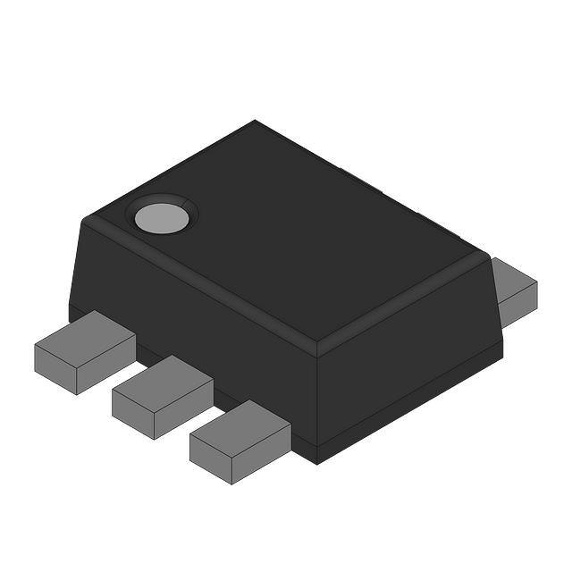
NPN low VCEsat Breakthrough In Small Signal (BISS) transistor in a SOT666 Surface
Mounted Device (SMD) plastic package.
PNP complement: PBSS5220V.
1.2 Features
Low collector-emitter saturation voltage VCEsat
High collector current capability: IC and ICM
High collector current gain (hFE) at high IC
High efficiency due to less heat generation
Smaller required Printed-Circuit Board (PCB) area than for conventional transistors
1.3 Applications
DC-to-DC conversion
MOSFET gate driving
Motor control
Charging circuits
Low power switches (e.g. motors, fans)
Portable applications
1.4 Quick reference data
Table 1.
Quick reference data
Symbol Parameter
Conditions
Min
Typ
Max
Unit
open base
-
-
20
V
-
-
2
A
-
-
4
A
-
140
175
mΩ
VCEO
collector-emitter voltage
IC
collector current
ICM
peak collector current
tp ≤ 300 μs
RCEsat
collector-emitter
saturation resistance
IC = 1 A;
IB = 100 mA
[1]
Pulse test: tp ≤ 300 μs; δ ≤ 0.02.
[1]
�PBSS4220V
NXP Semiconductors
20 V, 2 A NPN low VCEsat (BISS) transistor
2. Pinning information
Table 2.
Pinning
Pin
Description
1
collector
2
collector
3
base
4
emitter
5
collector
6
collector
Simplified outline
6
5
Symbol
1, 2, 5, 6
4
3
4
1
2
sym014
3
3. Ordering information
Table 3.
Ordering information
Type number
PBSS4220V
Package
Name
Description
Version
-
plastic surface mounted package; 6 leads
SOT666
4. Marking
Table 4.
Marking codes
Type number
Marking code
PBSS4220V
N6
5. Limiting values
Table 5.
Limiting values
In accordance with the Absolute Maximum Rating System (IEC 60134).
Symbol
Parameter
Conditions
Min
Max
Unit
VCBO
collector-base voltage
open emitter
-
20
V
VCEO
collector-emitter voltage
open base
-
20
V
VEBO
emitter-base voltage
open collector
-
5
V
IC
collector current
-
2
A
ICM
peak collector current
IB
base current
IBM
peak base current
tp ≤ 300 μs
total power dissipation
Tamb ≤ 25 °C
Ptot
Tj
tp ≤ 300 μs
junction temperature
PBSS4220V_2
Product data sheet
-
4
A
-
0.3
A
-
0.6
A
[1][4]
-
0.3
W
[2][4]
-
0.5
W
[3][4]
-
0.9
W
-
150
°C
© NXP B.V. 2009. All rights reserved.
Rev. 02 — 11 December 2009
2 of 13
�PBSS4220V
NXP Semiconductors
20 V, 2 A NPN low VCEsat (BISS) transistor
Table 5.
Limiting values …continued
In accordance with the Absolute Maximum Rating System (IEC 60134).
Symbol
Parameter
Tamb
Tstg
Conditions
Min
Max
Unit
ambient temperature
−65
+150
°C
storage temperature
−65
+150
°C
[1]
Device mounted on an FR4 PCB, single-sided copper, tin-plated and standard footprint.
[2]
Device mounted on an FR4 PCB, single-sided copper, tin-plated, mounting pad for collector 1 cm2.
[3]
Device mounted on a ceramic PCB, Al2O3, standard footprint.
[4]
Reflow soldering is the only recommended soldering method.
006aaa424
1.2
Ptot
(W)
(1)
0.8
(2)
0.4
(3)
0
0
40
80
120
160
Tamb (°C)
(1) Ceramic PCB, Al2O3, standard footprint
(2) FR4 PCB, mounting pad for collector 1 cm2
(3) FR4 PCB, standard footprint
Fig 1.
Power derating curves
PBSS4220V_2
Product data sheet
© NXP B.V. 2009. All rights reserved.
Rev. 02 — 11 December 2009
3 of 13
�PBSS4220V
NXP Semiconductors
20 V, 2 A NPN low VCEsat (BISS) transistor
6. Thermal characteristics
Table 6.
Thermal characteristics
Symbol
Parameter
thermal resistance from
junction to ambient
Rth(j-a)
Zth(j-a)
(K/W)
102
in free air
Min
Typ
Max
Unit
[1][4]
-
-
410
K/W
[2][4]
-
-
250
K/W
[3][4]
-
-
140
K/W
-
-
80
K/W
thermal resistance from
junction to solder point
Rth(j-sp)
103
Conditions
[1]
Device mounted on an FR4 PCB, single-sided copper, tin-plated and standard footprint.
[2]
Device mounted on an FR4 PCB, single-sided copper, tin-plated, mounting pad for collector 1 cm2.
[3]
Device mounted on a ceramic PCB, Al2O3, standard footprint.
[4]
Reflow soldering is the only recommended soldering method.
006aaa425
duty cycle =
1
0.75
0.5
0.33
0.2
0.1
0.05
10
1
0.02
0.01
0
10−1
10−5
10−4
10−3
10−2
10−1
1
10
102
103
t p (s)
FR4 PCB, standard footprint
Fig 2.
Transient thermal impedance from junction to ambient as a function of pulse time; typical values
PBSS4220V_2
Product data sheet
© NXP B.V. 2009. All rights reserved.
Rev. 02 — 11 December 2009
4 of 13
�PBSS4220V
NXP Semiconductors
20 V, 2 A NPN low VCEsat (BISS) transistor
7. Characteristics
Table 7.
Characteristics
Tamb = 25 °C unless otherwise specified.
Symbol Parameter
Conditions
Min
Typ
Max
Unit
collector-base cut-off
current
VCB = 20 V; IE = 0 A
-
-
0.1
μA
VCB = 20 V; IE = 0 A;
Tj = 150 °C
-
-
50
μA
ICES
collector-emitter cut-off
current
VCE = 20 V; VBE = 0 V
-
-
0.1
μA
IEBO
emitter-base cut-off
current
VEB = 5 V; IC = 0 A
-
-
0.1
μA
hFE
DC current gain
VCE = 2 V; IC = 1 mA
220
480
-
ICBO
VCE = 2 V; IC = 100 mA
VCEsat
collector-emitter
saturation voltage
220
440
-
VCE = 2 V; IC = 500 mA
[1]
220
410
-
VCE = 2 V; IC = 1 A
[1]
200
360
-
VCE = 2 V; IC = 2 A
[1]
120
220
-
-
35
55
mV
IC = 500 mA; IB = 50 mA
IC = 100 mA; IB = 1 mA
[1]
-
70
95
mV
IC = 1 A; IB = 50 mA
[1]
-
145
180
mV
IC = 1 A; IB = 100 mA
[1]
-
140
175
mV
IC = 2 A; IB = 100 mA
[1]
-
275
355
mV
IC = 2 A; IB = 200 mA
[1]
-
270
350
mV
175
mΩ
RCEsat
collector-emitter
saturation resistance
IC = 1 A; IB = 100 mA
[1]
-
140
VBEsat
base-emitter saturation IC = 1 A; IB = 50 mA
voltage
IC = 1 A; IB = 100 mA
[1]
-
0.95
1.1
V
[1]
-
1
1.2
V
VBEon
base-emitter turn-on
voltage
VCE = 5 V; IC = 1 A
-
0.8
1.1
V
IC = 1 A; IBon = 50 mA;
IBoff = −50 mA
-
9
-
ns
-
29
-
ns
td
delay time
tr
rise time
ton
turn-on time
-
38
-
ns
ts
storage time
-
200
-
ns
tf
fall time
-
40
-
ns
toff
turn-off time
-
240
-
ns
fT
transition frequency
VCE = 10 V; IC = 50 mA;
f = 100 MHz
-
210
-
MHz
Cc
collector capacitance
VCB = 10 V; IE = ie = 0 A;
f = 1 MHz
-
11
-
pF
[1]
Pulse test: tp ≤ 300 μs; δ ≤ 0.02.
PBSS4220V_2
Product data sheet
© NXP B.V. 2009. All rights reserved.
Rev. 02 — 11 December 2009
5 of 13
�PBSS4220V
NXP Semiconductors
20 V, 2 A NPN low VCEsat (BISS) transistor
006aaa662
1000
hFE
006aaa663
1.0
VBE
(V)
800
0.8
(1)
0.6
(2)
(1)
600
(2)
400
(3)
(3)
0.4
200
0
10−1
1
10
102
0.2
10−1
103
104
IC (mA)
1
VCE = 2 V
VCE = 5 V
(1) Tamb = 100 °C
(1) Tamb = −55 °C
(2) Tamb = 25 °C
(2) Tamb = 25 °C
(3) Tamb = −55 °C
Fig 3.
10
102
103
104
IC (mA)
(3) Tamb = 100 °C
DC current gain as a function of collector
current; typical values
Fig 4.
006aaa664
1
VCEsat
(V)
Base-emitter voltage as a function of collector
current; typical values
006aaa665
1
VCEsat
(V)
10−1
10−1
(1)
(2)
(3)
(1)
(2)
10−2
10−2
(3)
10−3
10−1
1
10
102
103
104
IC (mA)
10−3
10−1
1
(1) Tamb = 100 °C
(1) IC/IB = 100
(2) Tamb = 25 °C
(2) IC/IB = 50
(3) Tamb = −55 °C
(3) IC/IB = 10
Collector-emitter saturation voltage as a
function of collector current; typical values
Fig 6.
103
104
IC (mA)
Collector-emitter saturation voltage as a
function of collector current; typical values
PBSS4220V_2
Product data sheet
102
Tamb = 25 °C
IC/IB = 20
Fig 5.
10
© NXP B.V. 2009. All rights reserved.
Rev. 02 — 11 December 2009
6 of 13
�PBSS4220V
NXP Semiconductors
20 V, 2 A NPN low VCEsat (BISS) transistor
006aaa666
1.2
VBEsat
(V)
006aaa667
102
RCEsat
(Ω)
1.0
(1)
10
0.8
(2)
(3)
0.6
1
0.4
(1)
(2)
(3)
0.2
10−1
1
10
102
103
104
IC (mA)
10−1
10−1
IC/IB = 20
1
10
(1) Tamb = −55 °C
(1) Tamb = 100 °C
(2) Tamb = 25 °C
(3) Tamb = 100 °C
(3) Tamb = −55 °C
Base-emitter saturation voltage as a function
of collector current; typical values
006aaa668
2.0
IB (mA) = 8.0
IC
(A)
103
104
IC (mA)
IC/IB = 20
(2) Tamb = 25 °C
Fig 7.
102
7.2
6.4
Collector-emitter saturation resistance as a
function of collector current; typical values
006aaa669
103
RCEsat
(Ω)
5.6
1.6
Fig 8.
102
4.8
4.0
(1)
1.2
3.2
10
2.4
(2)
0.8
1.6
1
0.4
(3)
0.8
0
0
1
2
3
4
5
10−1
10−1
1
VCE (V)
Tamb = 25 °C
10
102
103
104
IC (mA)
Tamb = 25 °C
(1) IC/IB = 100
(2) IC/IB = 50
(3) IC/IB = 10
Fig 9.
Collector current as a function of
collector-emitter voltage; typical values
Fig 10. Collector-emitter saturation resistance as a
function of collector current; typical values
PBSS4220V_2
Product data sheet
© NXP B.V. 2009. All rights reserved.
Rev. 02 — 11 December 2009
7 of 13
�PBSS4220V
NXP Semiconductors
20 V, 2 A NPN low VCEsat (BISS) transistor
8. Test information
IB
input pulse
(idealized waveform)
90 %
IBon (100 %)
10 %
IBoff
output pulse
(idealized waveform)
IC
90 %
IC (100 %)
10 %
t
td
ts
tr
ton
tf
toff
006aaa003
Fig 11. BISS transistor switching time definition
VBB
RB
VCC
RC
Vo
(probe)
oscilloscope
450 Ω
(probe)
450 Ω
oscilloscope
R2
VI
DUT
R1
mlb826
IC = 1 A; IBon = 50 mA; IBoff = −50 mA; R1 = open; R2 = 45 Ω; RB = 145 Ω; RC = 10 Ω
Fig 12. Test circuit for switching times
PBSS4220V_2
Product data sheet
© NXP B.V. 2009. All rights reserved.
Rev. 02 — 11 December 2009
8 of 13
�PBSS4220V
NXP Semiconductors
20 V, 2 A NPN low VCEsat (BISS) transistor
9. Package outline
1.7
1.5
6
0.6
0.5
5
4
0.3
0.1
1.7
1.5
1.3
1.1
pin 1 index
1
2
3
0.27
0.17
0.5
0.18
0.08
1
Dimensions in mm
04-11-08
Fig 13. Package outline SOT666
10. Packing information
Table 8.
Packing methods
The indicated -xxx are the last three digits of the 12NC ordering code.[1]
Type number
Package
Description
Packing quantity
4000
PBSS4220V
[1]
SOT666
2 mm pitch, 8 mm tape and reel
-
-315
4 mm pitch, 8 mm tape and reel
-115
-
For further information and the availability of packing methods, see Section 14.
PBSS4220V_2
Product data sheet
8000
© NXP B.V. 2009. All rights reserved.
Rev. 02 — 11 December 2009
9 of 13
�PBSS4220V
NXP Semiconductors
20 V, 2 A NPN low VCEsat (BISS) transistor
11. Soldering
2.75
2.45
2.1
1.6
solder lands
0.4
(6×) 0.25
(2×)
0.538
2
1.7 1.075
0.3
(2×)
0.55
(2×)
placement area
solder paste
occupied area
0.325 0.375
(4×) (4×)
Dimensions in mm
1.7
0.45
(4×)
0.6
(2×)
0.5
(4×)
0.65
(2×)
sot666_fr
Reflow soldering is the only recommended soldering method.
Fig 14. Reflow soldering footprint
PBSS4220V_2
Product data sheet
© NXP B.V. 2009. All rights reserved.
Rev. 02 — 11 December 2009
10 of 13
�PBSS4220V
NXP Semiconductors
20 V, 2 A NPN low VCEsat (BISS) transistor
12. Revision history
Table 9.
Revision history
Document ID
Release date
Data sheet status
Change notice
Supersedes
PBSS4220V_2
20091211
Product data sheet
-
PBSS4220V_1
Modifications:
PBSS4220V_1
•
This data sheet was changed to reflect the new company name NXP Semiconductors,
including new legal definitions and disclaimers. No changes were made to the technical
content.
•
Figure 14 “Reflow soldering footprint”: updated
20060206
Product data sheet
-
PBSS4220V_2
Product data sheet
-
© NXP B.V. 2009. All rights reserved.
Rev. 02 — 11 December 2009
11 of 13
�PBSS4220V
NXP Semiconductors
20 V, 2 A NPN low VCEsat (BISS) transistor
13. Legal information
13.1 Data sheet status
Document status[1][2]
Product status[3]
Objective [short] data sheet
Development
This document contains data from the objective specification for product development.
Preliminary [short] data sheet
Qualification
This document contains data from the preliminary specification.
Product [short] data sheet
Production
This document contains the product specification.
Definition
[1]
Please consult the most recently issued document before initiating or completing a design.
[2]
The term ‘short data sheet’ is explained in section “Definitions”.
[3]
The product status of device(s) described in this document may have changed since this document was published and may differ in case of multiple devices. The latest product status
information is available on the Internet at URL http://www.nxp.com.
13.2 Definitions
Draft — The document is a draft version only. The content is still under
internal review and subject to formal approval, which may result in
modifications or additions. NXP Semiconductors does not give any
representations or warranties as to the accuracy or completeness of
information included herein and shall have no liability for the consequences of
use of such information.
Short data sheet — A short data sheet is an extract from a full data sheet
with the same product type number(s) and title. A short data sheet is intended
for quick reference only and should not be relied upon to contain detailed and
full information. For detailed and full information see the relevant full data
sheet, which is available on request via the local NXP Semiconductors sales
office. In case of any inconsistency or conflict with the short data sheet, the
full data sheet shall prevail.
13.3 Disclaimers
General — Information in this document is believed to be accurate and
reliable. However, NXP Semiconductors does not give any representations or
warranties, expressed or implied, as to the accuracy or completeness of such
information and shall have no liability for the consequences of use of such
information.
Right to make changes — NXP Semiconductors reserves the right to make
changes to information published in this document, including without
limitation specifications and product descriptions, at any time and without
notice. This document supersedes and replaces all information supplied prior
to the publication hereof.
Suitability for use — NXP Semiconductors products are not designed,
authorized or warranted to be suitable for use in medical, military, aircraft,
space or life support equipment, nor in applications where failure or
malfunction of an NXP Semiconductors product can reasonably be expected
to result in personal injury, death or severe property or environmental
damage. NXP Semiconductors accepts no liability for inclusion and/or use of
NXP Semiconductors products in such equipment or applications and
therefore such inclusion and/or use is at the customer’s own risk.
Applications — Applications that are described herein for any of these
products are for illustrative purposes only. NXP Semiconductors makes no
representation or warranty that such applications will be suitable for the
specified use without further testing or modification.
Limiting values — Stress above one or more limiting values (as defined in
the Absolute Maximum Ratings System of IEC 60134) may cause permanent
damage to the device. Limiting values are stress ratings only and operation of
the device at these or any other conditions above those given in the
Characteristics sections of this document is not implied. Exposure to limiting
values for extended periods may affect device reliability.
Terms and conditions of sale — NXP Semiconductors products are sold
subject to the general terms and conditions of commercial sale, as published
at http://www.nxp.com/profile/terms, including those pertaining to warranty,
intellectual property rights infringement and limitation of liability, unless
explicitly otherwise agreed to in writing by NXP Semiconductors. In case of
any inconsistency or conflict between information in this document and such
terms and conditions, the latter will prevail.
No offer to sell or license — Nothing in this document may be interpreted or
construed as an offer to sell products that is open for acceptance or the grant,
conveyance or implication of any license under any copyrights, patents or
other industrial or intellectual property rights.
Export control — This document as well as the item(s) described herein
may be subject to export control regulations. Export might require a prior
authorization from national authorities.
Quick reference data — The Quick reference data is an extract of the
product data given in the Limiting values and Characteristics sections of this
document, and as such is not complete, exhaustive or legally binding.
13.4 Trademarks
Notice: All referenced brands, product names, service names and trademarks
are the property of their respective owners.
14. Contact information
For more information, please visit: http://www.nxp.com
For sales office addresses, please send an email to: salesaddresses@nxp.com
PBSS4220V_2
Product data sheet
© NXP B.V. 2009. All rights reserved.
Rev. 02 — 11 December 2009
12 of 13
�PBSS4220V
NXP Semiconductors
20 V, 2 A NPN low VCEsat (BISS) transistor
15. Contents
1
1.1
1.2
1.3
1.4
2
3
4
5
6
7
8
9
10
11
12
13
13.1
13.2
13.3
13.4
14
15
Product profile . . . . . . . . . . . . . . . . . . . . . . . . . . 1
General description . . . . . . . . . . . . . . . . . . . . . 1
Features . . . . . . . . . . . . . . . . . . . . . . . . . . . . . . 1
Applications . . . . . . . . . . . . . . . . . . . . . . . . . . . 1
Quick reference data . . . . . . . . . . . . . . . . . . . . 1
Pinning information . . . . . . . . . . . . . . . . . . . . . . 2
Ordering information . . . . . . . . . . . . . . . . . . . . . 2
Marking . . . . . . . . . . . . . . . . . . . . . . . . . . . . . . . . 2
Limiting values. . . . . . . . . . . . . . . . . . . . . . . . . . 2
Thermal characteristics . . . . . . . . . . . . . . . . . . 4
Characteristics . . . . . . . . . . . . . . . . . . . . . . . . . . 5
Test information . . . . . . . . . . . . . . . . . . . . . . . . . 8
Package outline . . . . . . . . . . . . . . . . . . . . . . . . . 9
Packing information . . . . . . . . . . . . . . . . . . . . . 9
Soldering . . . . . . . . . . . . . . . . . . . . . . . . . . . . . 10
Revision history . . . . . . . . . . . . . . . . . . . . . . . . 11
Legal information. . . . . . . . . . . . . . . . . . . . . . . 12
Data sheet status . . . . . . . . . . . . . . . . . . . . . . 12
Definitions . . . . . . . . . . . . . . . . . . . . . . . . . . . . 12
Disclaimers . . . . . . . . . . . . . . . . . . . . . . . . . . . 12
Trademarks. . . . . . . . . . . . . . . . . . . . . . . . . . . 12
Contact information. . . . . . . . . . . . . . . . . . . . . 12
Contents . . . . . . . . . . . . . . . . . . . . . . . . . . . . . . 13
Please be aware that important notices concerning this document and the product(s)
described herein, have been included in section ‘Legal information’.
© NXP B.V. 2009.
All rights reserved.
For more information, please visit: http://www.nxp.com
For sales office addresses, please send an email to: salesaddresses@nxp.com
Date of release: 11 December 2009
Document identifier: PBSS4220V_2
�


 工商网监
湘ICP备2023018690号
工商网监
湘ICP备2023018690号
