MC9S12HY64
Reference Manual
Covers MC9S12HY/HA Family
S12
Microcontrollers
MC9S12HY64RMV1
Rev. 1.05
09/2012
freescale.com
�To provide the most up-to-date information, the revision of our documents on the World Wide Web will be
the most current. Your printed copy may be an earlier revision. To verify you have the latest information
available, refer to:
freescale.com
A full list of family members and options is included in the appendices.
The following revision history table summarizes changes contained in this document.
This document contains information for all constituent modules, with the exception of the CPU. For CPU
information please refer to CPU12-1 in the CPU12 & CPU12X Reference Manual.
Revision History
Date
Revision
Level
July, 2009
1.00
initial v1.00 version
Aug, 2009
1.01
update SCI block guide, update motor pad input leakage in Appendix A
Nov, 2009
1.02
update FTMRC block guide, update MC10B8C block guide, minor update in
chapter 1, minor typo correction in Appendix F
May, 2010
1.03
update PIM block guide, update CPMU block guide, update TIM block guide
Nov, 2010
1.04
update SCI block guide, update typo in device overview
Sep, 2012
1.05
update Device overview, PIM, BDM, DBG, CPMU, INT, PWM and Appendix
for Bandgap and Motor/LCD pad maximum value update
Description
�Chapter 1
Device Overview MC9S12HY/HA-Family . . . . . . . . . . . . . . . . . 11
Chapter 2
Port Integration Module (S12HYPIMV1) . . . . . . . . . . . . . . . . . . 53
Chapter 3
S12P Memory Map Control (S12PMMCV1). . . . . . . . . . . . . . . 135
Chapter 4
Interrupt Module (S12SINTV1). . . . . . . . . . . . . . . . . . . . . . . . . 151
Chapter 5
Background Debug Module (S12SBDMV1) . . . . . . . . . . . . . . 159
Chapter 6
S12S Debug Module (S12SDBGV2) . . . . . . . . . . . . . . . . . . . . 183
Chapter 7
227
S12 Clock, Reset and Power Management Unit (S12CPMU) . . .
Chapter 8
Analog-to-Digital Converter (ADC12B8CV1) . . . . . . . . . . . . . 285
Chapter 9
311
Freescale’s Scalable Controller Area Network (S12MSCANV3).
Chapter 10
Inter-Integrated Circuit (IICV3) . . . . . . . . . . . . . . . . . . . . . . . . 365
Chapter 11
Pulse-Width Modulator (S12PWM8B8CV1) . . . . . . . . . . . . . . 393
Chapter 12
Serial Communication Interface (S12SCIV5) . . . . . . . . . . . . . 425
Chapter 13
Serial Peripheral Interface (S12SPIV5) . . . . . . . . . . . . . . . . . . 463
Chapter 14
Timer Module (TIM16B8CV2) . . . . . . . . . . . . . . . . . . . . . . . . . 489
Chapter 15
32 KByte Flash Module (S12FTMRC32K1V1). . . . . . . . . . . . . 517
Chapter 16
48 KByte Flash Module (S12FTMRC48K1V1). . . . . . . . . . . . . 567
Chapter 17
64 KByte Flash Module (S12FTMRC64K1V1). . . . . . . . . . . . . 617
Chapter 18
Liquid Crystal Display (LCD40F4BV1) . . . . . . . . . . . . . . . . . . 667
Chapter 19
Motor Controller (MC10B8CV1). . . . . . . . . . . . . . . . . . . . . . . . 689
Appendix A Electrical Characteristics. . . . . . . . . . . . . . . . . . . . . . . . . . . . . 721
Appendix B Ordering Information . . . . . . . . . . . . . . . . . . . . . . . . . . . . . . . . 756
Appendix C Package Information . . . . . . . . . . . . . . . . . . . . . . . . . . . . . . . . 757
Appendix D PCB Layout Guidelines . . . . . . . . . . . . . . . . . . . . . . . . . . . . . . 763
MC9S12HY/HA-Family Reference Manual, Rev. 1.05
Freescale Semiconductor
3
�Appendix E Derivative Differences . . . . . . . . . . . . . . . . . . . . . . . . . . . . . . . 767
Appendix F Detailed Register Address Map. . . . . . . . . . . . . . . . . . . . . . . . 768
MC9S12HY/HA-Family Reference Manual, Rev. 1.05
4
Freescale Semiconductor
�Chapter 1
Device Overview MC9S12HY/HA-Family
1.1
1.2
1.3
1.4
1.5
1.6
1.7
1.8
1.9
1.10
1.11
1.12
1.13
1.14
1.15
Introduction . . . . . . . . . . . . . . . . . . . . . . . . . . . . . . . . . . . . . . . . . . . . . . . . . . . . . . . . . . . . . . . . . . 11
Features . . . . . . . . . . . . . . . . . . . . . . . . . . . . . . . . . . . . . . . . . . . . . . . . . . . . . . . . . . . . . . . . . . . . . 11
Module Features . . . . . . . . . . . . . . . . . . . . . . . . . . . . . . . . . . . . . . . . . . . . . . . . . . . . . . . . . . . . . . . 13
Block Diagram . . . . . . . . . . . . . . . . . . . . . . . . . . . . . . . . . . . . . . . . . . . . . . . . . . . . . . . . . . . . . . . . 19
Device Memory Map . . . . . . . . . . . . . . . . . . . . . . . . . . . . . . . . . . . . . . . . . . . . . . . . . . . . . . . . . . . 20
Part ID Assignments . . . . . . . . . . . . . . . . . . . . . . . . . . . . . . . . . . . . . . . . . . . . . . . . . . . . . . . . . . . . 25
Signal Description . . . . . . . . . . . . . . . . . . . . . . . . . . . . . . . . . . . . . . . . . . . . . . . . . . . . . . . . . . . . . 25
System Clock Description . . . . . . . . . . . . . . . . . . . . . . . . . . . . . . . . . . . . . . . . . . . . . . . . . . . . . . . 45
Modes of Operation . . . . . . . . . . . . . . . . . . . . . . . . . . . . . . . . . . . . . . . . . . . . . . . . . . . . . . . . . . . . 46
Security . . . . . . . . . . . . . . . . . . . . . . . . . . . . . . . . . . . . . . . . . . . . . . . . . . . . . . . . . . . . . . . . . . . . . . 46
Resets and Interrupts . . . . . . . . . . . . . . . . . . . . . . . . . . . . . . . . . . . . . . . . . . . . . . . . . . . . . . . . . . . 47
COP Configuration . . . . . . . . . . . . . . . . . . . . . . . . . . . . . . . . . . . . . . . . . . . . . . . . . . . . . . . . . . . . . 50
ATD External Trigger Input Connection . . . . . . . . . . . . . . . . . . . . . . . . . . . . . . . . . . . . . . . . . . . . 50
S12CPMU Configuration . . . . . . . . . . . . . . . . . . . . . . . . . . . . . . . . . . . . . . . . . . . . . . . . . . . . . . . . 51
Documentation Note . . . . . . . . . . . . . . . . . . . . . . . . . . . . . . . . . . . . . . . . . . . . . . . . . . . . . . . . . . . 51
Chapter 2
Port Integration Module (S12HYPIMV1)
2.1
2.2
2.3
2.4
2.5
Introduction . . . . . . . . . . . . . . . . . . . . . . . . . . . . . . . . . . . . . . . . . . . . . . . . . . . . . . . . . . . . . . . . . . 53
External Signal Description . . . . . . . . . . . . . . . . . . . . . . . . . . . . . . . . . . . . . . . . . . . . . . . . . . . . . . 54
Memory Map and Register Definition . . . . . . . . . . . . . . . . . . . . . . . . . . . . . . . . . . . . . . . . . . . . . . 59
Functional Description . . . . . . . . . . . . . . . . . . . . . . . . . . . . . . . . . . . . . . . . . . . . . . . . . . . . . . . . . 127
Initialization Information . . . . . . . . . . . . . . . . . . . . . . . . . . . . . . . . . . . . . . . . . . . . . . . . . . . . . . . 133
Chapter 3S12P Memory Map Control (S12PMMCV1)
3.1
3.2
3.3
3.4
3.5
3.6
Introduction . . . . . . . . . . . . . . . . . . . . . . . . . . . . . . . . . . . . . . . . . . . . . . . . . . . . . . . . . . . . . . . . . 135
External Signal Description . . . . . . . . . . . . . . . . . . . . . . . . . . . . . . . . . . . . . . . . . . . . . . . . . . . . . 137
Memory Map and Registers . . . . . . . . . . . . . . . . . . . . . . . . . . . . . . . . . . . . . . . . . . . . . . . . . . . . . 137
Functional Description . . . . . . . . . . . . . . . . . . . . . . . . . . . . . . . . . . . . . . . . . . . . . . . . . . . . . . . . . 141
Implemented Memory in the System Memory Architecture . . . . . . . . . . . . . . . . . . . . . . . . . . . . 145
Initialization/Application Information . . . . . . . . . . . . . . . . . . . . . . . . . . . . . . . . . . . . . . . . . . . . . 148
Chapter 4
Interrupt Module (S12SINTV1)
4.1
4.2
4.3
4.4
Introduction . . . . . . . . . . . . . . . . . . . . . . . . . . . . . . . . . . . . . . . . . . . . . . . . . . . . . . . . . . . . . . . . . 151
External Signal Description . . . . . . . . . . . . . . . . . . . . . . . . . . . . . . . . . . . . . . . . . . . . . . . . . . . . . 153
Memory Map and Register Definition . . . . . . . . . . . . . . . . . . . . . . . . . . . . . . . . . . . . . . . . . . . . . 153
Functional Description . . . . . . . . . . . . . . . . . . . . . . . . . . . . . . . . . . . . . . . . . . . . . . . . . . . . . . . . . 154
MC9S12HY/HA-Family Reference Manual, Rev. 1.05
Freescale Semiconductor
5
�4.5
Initialization/Application Information . . . . . . . . . . . . . . . . . . . . . . . . . . . . . . . . . . . . . . . . . . . . . 156
Chapter 5
Background Debug Module (S12SBDMV1)
5.1
5.2
5.3
5.4
Introduction . . . . . . . . . . . . . . . . . . . . . . . . . . . . . . . . . . . . . . . . . . . . . . . . . . . . . . . . . . . . . . . . . 159
External Signal Description . . . . . . . . . . . . . . . . . . . . . . . . . . . . . . . . . . . . . . . . . . . . . . . . . . . . . 161
Memory Map and Register Definition . . . . . . . . . . . . . . . . . . . . . . . . . . . . . . . . . . . . . . . . . . . . . 161
Functional Description . . . . . . . . . . . . . . . . . . . . . . . . . . . . . . . . . . . . . . . . . . . . . . . . . . . . . . . . . 165
Chapter 6
S12S Debug Module (S12SDBGV2)
6.1
6.2
6.3
6.4
6.5
Introduction . . . . . . . . . . . . . . . . . . . . . . . . . . . . . . . . . . . . . . . . . . . . . . . . . . . . . . . . . . . . . . . . . 183
External Signal Description . . . . . . . . . . . . . . . . . . . . . . . . . . . . . . . . . . . . . . . . . . . . . . . . . . . . . 185
Memory Map and Registers . . . . . . . . . . . . . . . . . . . . . . . . . . . . . . . . . . . . . . . . . . . . . . . . . . . . . 186
Functional Description . . . . . . . . . . . . . . . . . . . . . . . . . . . . . . . . . . . . . . . . . . . . . . . . . . . . . . . . . 204
Application Information . . . . . . . . . . . . . . . . . . . . . . . . . . . . . . . . . . . . . . . . . . . . . . . . . . . . . . . . 220
Chapter 7
S12 Clock, Reset and Power Management Unit (S12CPMU) Block Description
7.1
7.2
7.3
7.4
7.5
7.6
7.7
Introduction . . . . . . . . . . . . . . . . . . . . . . . . . . . . . . . . . . . . . . . . . . . . . . . . . . . . . . . . . . . . . . . . . 228
Signal Description . . . . . . . . . . . . . . . . . . . . . . . . . . . . . . . . . . . . . . . . . . . . . . . . . . . . . . . . . . . . 234
Memory Map and Registers . . . . . . . . . . . . . . . . . . . . . . . . . . . . . . . . . . . . . . . . . . . . . . . . . . . . . 236
Functional Description . . . . . . . . . . . . . . . . . . . . . . . . . . . . . . . . . . . . . . . . . . . . . . . . . . . . . . . . . 271
Resets . . . . . . . . . . . . . . . . . . . . . . . . . . . . . . . . . . . . . . . . . . . . . . . . . . . . . . . . . . . . . . . . . . . . . . 280
Interrupts . . . . . . . . . . . . . . . . . . . . . . . . . . . . . . . . . . . . . . . . . . . . . . . . . . . . . . . . . . . . . . . . . . . 282
Initialization/Application Information . . . . . . . . . . . . . . . . . . . . . . . . . . . . . . . . . . . . . . . . . . . . . 284
Chapter 8
Analog-to-Digital Converter (ADC12B8CV1)
Block Description
8.1
8.2
8.3
8.4
8.5
8.6
Introduction . . . . . . . . . . . . . . . . . . . . . . . . . . . . . . . . . . . . . . . . . . . . . . . . . . . . . . . . . . . . . . . . . 285
Signal Description . . . . . . . . . . . . . . . . . . . . . . . . . . . . . . . . . . . . . . . . . . . . . . . . . . . . . . . . . . . . 289
Memory Map and Register Definition . . . . . . . . . . . . . . . . . . . . . . . . . . . . . . . . . . . . . . . . . . . . . 289
Functional Description . . . . . . . . . . . . . . . . . . . . . . . . . . . . . . . . . . . . . . . . . . . . . . . . . . . . . . . . . 307
Resets . . . . . . . . . . . . . . . . . . . . . . . . . . . . . . . . . . . . . . . . . . . . . . . . . . . . . . . . . . . . . . . . . . . . . . 308
Interrupts . . . . . . . . . . . . . . . . . . . . . . . . . . . . . . . . . . . . . . . . . . . . . . . . . . . . . . . . . . . . . . . . . . . 309
Chapter 9
Freescale’s Scalable Controller Area Network (S12MSCANV3)
9.1
9.2
9.3
9.4
Introduction . . . . . . . . . . . . . . . . . . . . . . . . . . . . . . . . . . . . . . . . . . . . . . . . . . . . . . . . . . . . . . . . . 311
External Signal Description . . . . . . . . . . . . . . . . . . . . . . . . . . . . . . . . . . . . . . . . . . . . . . . . . . . . . 314
Memory Map and Register Definition . . . . . . . . . . . . . . . . . . . . . . . . . . . . . . . . . . . . . . . . . . . . . 315
Functional Description . . . . . . . . . . . . . . . . . . . . . . . . . . . . . . . . . . . . . . . . . . . . . . . . . . . . . . . . . 347
MC9S12HY/HA-Family Reference Manual, Rev. 1.05
6
Freescale Semiconductor
�9.5
Initialization/Application Information . . . . . . . . . . . . . . . . . . . . . . . . . . . . . . . . . . . . . . . . . . . . . 364
Chapter 10
Inter-Integrated Circuit (IICV3) Block Description
10.1
10.2
10.3
10.4
10.5
10.6
10.7
Introduction . . . . . . . . . . . . . . . . . . . . . . . . . . . . . . . . . . . . . . . . . . . . . . . . . . . . . . . . . . . . . . . . . 365
External Signal Description . . . . . . . . . . . . . . . . . . . . . . . . . . . . . . . . . . . . . . . . . . . . . . . . . . . . . 368
Memory Map and Register Definition . . . . . . . . . . . . . . . . . . . . . . . . . . . . . . . . . . . . . . . . . . . . . 368
Functional Description . . . . . . . . . . . . . . . . . . . . . . . . . . . . . . . . . . . . . . . . . . . . . . . . . . . . . . . . . 380
Resets . . . . . . . . . . . . . . . . . . . . . . . . . . . . . . . . . . . . . . . . . . . . . . . . . . . . . . . . . . . . . . . . . . . . . . 385
Interrupts . . . . . . . . . . . . . . . . . . . . . . . . . . . . . . . . . . . . . . . . . . . . . . . . . . . . . . . . . . . . . . . . . . . 385
Application Information . . . . . . . . . . . . . . . . . . . . . . . . . . . . . . . . . . . . . . . . . . . . . . . . . . . . . . . . 386
Chapter 11
Pulse-Width Modulator (S12PWM8B8CV1)
11.1
11.2
11.3
11.4
11.5
11.6
Introduction . . . . . . . . . . . . . . . . . . . . . . . . . . . . . . . . . . . . . . . . . . . . . . . . . . . . . . . . . . . . . . . . . 393
External Signal Description . . . . . . . . . . . . . . . . . . . . . . . . . . . . . . . . . . . . . . . . . . . . . . . . . . . . . 394
Memory Map and Register Definition . . . . . . . . . . . . . . . . . . . . . . . . . . . . . . . . . . . . . . . . . . . . . 395
Functional Description . . . . . . . . . . . . . . . . . . . . . . . . . . . . . . . . . . . . . . . . . . . . . . . . . . . . . . . . . 411
Resets . . . . . . . . . . . . . . . . . . . . . . . . . . . . . . . . . . . . . . . . . . . . . . . . . . . . . . . . . . . . . . . . . . . . . . 422
Interrupts . . . . . . . . . . . . . . . . . . . . . . . . . . . . . . . . . . . . . . . . . . . . . . . . . . . . . . . . . . . . . . . . . . . 423
Chapter 12
Serial Communication Interface (S12SCIV5)
12.1
12.2
12.3
12.4
12.5
Introduction . . . . . . . . . . . . . . . . . . . . . . . . . . . . . . . . . . . . . . . . . . . . . . . . . . . . . . . . . . . . . . . . . 425
External Signal Description . . . . . . . . . . . . . . . . . . . . . . . . . . . . . . . . . . . . . . . . . . . . . . . . . . . . . 428
Memory Map and Register Definition . . . . . . . . . . . . . . . . . . . . . . . . . . . . . . . . . . . . . . . . . . . . . 428
Functional Description . . . . . . . . . . . . . . . . . . . . . . . . . . . . . . . . . . . . . . . . . . . . . . . . . . . . . . . . . 441
Initialization/Application Information . . . . . . . . . . . . . . . . . . . . . . . . . . . . . . . . . . . . . . . . . . . . . 459
Chapter 13
Serial Peripheral Interface (S12SPIV5)
13.1
13.2
13.3
13.4
Introduction . . . . . . . . . . . . . . . . . . . . . . . . . . . . . . . . . . . . . . . . . . . . . . . . . . . . . . . . . . . . . . . . . 463
External Signal Description . . . . . . . . . . . . . . . . . . . . . . . . . . . . . . . . . . . . . . . . . . . . . . . . . . . . . 465
Memory Map and Register Definition . . . . . . . . . . . . . . . . . . . . . . . . . . . . . . . . . . . . . . . . . . . . . 466
Functional Description . . . . . . . . . . . . . . . . . . . . . . . . . . . . . . . . . . . . . . . . . . . . . . . . . . . . . . . . . 475
Chapter 14
Timer Module (TIM16B8CV2) Block Description
14.1
14.2
14.3
14.4
14.5
14.6
Introduction . . . . . . . . . . . . . . . . . . . . . . . . . . . . . . . . . . . . . . . . . . . . . . . . . . . . . . . . . . . . . . . . . 489
External Signal Description . . . . . . . . . . . . . . . . . . . . . . . . . . . . . . . . . . . . . . . . . . . . . . . . . . . . . 493
Memory Map and Register Definition . . . . . . . . . . . . . . . . . . . . . . . . . . . . . . . . . . . . . . . . . . . . . 494
Functional Description . . . . . . . . . . . . . . . . . . . . . . . . . . . . . . . . . . . . . . . . . . . . . . . . . . . . . . . . . 511
Resets . . . . . . . . . . . . . . . . . . . . . . . . . . . . . . . . . . . . . . . . . . . . . . . . . . . . . . . . . . . . . . . . . . . . . . 515
Interrupts . . . . . . . . . . . . . . . . . . . . . . . . . . . . . . . . . . . . . . . . . . . . . . . . . . . . . . . . . . . . . . . . . . . 515
MC9S12HY/HA-Family Reference Manual, Rev. 1.05
Freescale Semiconductor
7
�Chapter 15
32 KByte Flash Module (S12FTMRC32K1V1)
15.1
15.2
15.3
15.4
15.5
15.6
Introduction . . . . . . . . . . . . . . . . . . . . . . . . . . . . . . . . . . . . . . . . . . . . . . . . . . . . . . . . . . . . . . . . . 517
External Signal Description . . . . . . . . . . . . . . . . . . . . . . . . . . . . . . . . . . . . . . . . . . . . . . . . . . . . . 520
Memory Map and Registers . . . . . . . . . . . . . . . . . . . . . . . . . . . . . . . . . . . . . . . . . . . . . . . . . . . . . 521
Functional Description . . . . . . . . . . . . . . . . . . . . . . . . . . . . . . . . . . . . . . . . . . . . . . . . . . . . . . . . . 543
Security . . . . . . . . . . . . . . . . . . . . . . . . . . . . . . . . . . . . . . . . . . . . . . . . . . . . . . . . . . . . . . . . . . . . . 564
Initialization . . . . . . . . . . . . . . . . . . . . . . . . . . . . . . . . . . . . . . . . . . . . . . . . . . . . . . . . . . . . . . . . . 566
Chapter 16
48 KByte Flash Module (S12FTMRC48K1V1)
16.1
16.2
16.3
16.4
16.5
16.6
Introduction . . . . . . . . . . . . . . . . . . . . . . . . . . . . . . . . . . . . . . . . . . . . . . . . . . . . . . . . . . . . . . . . . 567
External Signal Description . . . . . . . . . . . . . . . . . . . . . . . . . . . . . . . . . . . . . . . . . . . . . . . . . . . . . 570
Memory Map and Registers . . . . . . . . . . . . . . . . . . . . . . . . . . . . . . . . . . . . . . . . . . . . . . . . . . . . . 571
Functional Description . . . . . . . . . . . . . . . . . . . . . . . . . . . . . . . . . . . . . . . . . . . . . . . . . . . . . . . . . 592
Security . . . . . . . . . . . . . . . . . . . . . . . . . . . . . . . . . . . . . . . . . . . . . . . . . . . . . . . . . . . . . . . . . . . . . 613
Initialization . . . . . . . . . . . . . . . . . . . . . . . . . . . . . . . . . . . . . . . . . . . . . . . . . . . . . . . . . . . . . . . . . 615
Chapter 17
64 KByte Flash Module (S12FTMRC64K1V1)
17.1
17.2
17.3
17.4
17.5
17.6
Introduction . . . . . . . . . . . . . . . . . . . . . . . . . . . . . . . . . . . . . . . . . . . . . . . . . . . . . . . . . . . . . . . . . 617
External Signal Description . . . . . . . . . . . . . . . . . . . . . . . . . . . . . . . . . . . . . . . . . . . . . . . . . . . . . 620
Memory Map and Registers . . . . . . . . . . . . . . . . . . . . . . . . . . . . . . . . . . . . . . . . . . . . . . . . . . . . . 621
Functional Description . . . . . . . . . . . . . . . . . . . . . . . . . . . . . . . . . . . . . . . . . . . . . . . . . . . . . . . . . 643
Security . . . . . . . . . . . . . . . . . . . . . . . . . . . . . . . . . . . . . . . . . . . . . . . . . . . . . . . . . . . . . . . . . . . . . 664
Initialization . . . . . . . . . . . . . . . . . . . . . . . . . . . . . . . . . . . . . . . . . . . . . . . . . . . . . . . . . . . . . . . . . 666
Chapter 18
Liquid Crystal Display (LCD40F4BV1) Block Description
18.1
18.2
18.3
18.4
18.5
18.6
Introduction . . . . . . . . . . . . . . . . . . . . . . . . . . . . . . . . . . . . . . . . . . . . . . . . . . . . . . . . . . . . . . . . . 667
External Signal Description . . . . . . . . . . . . . . . . . . . . . . . . . . . . . . . . . . . . . . . . . . . . . . . . . . . . . 670
Memory Map and Register Definition . . . . . . . . . . . . . . . . . . . . . . . . . . . . . . . . . . . . . . . . . . . . . 670
Functional Description . . . . . . . . . . . . . . . . . . . . . . . . . . . . . . . . . . . . . . . . . . . . . . . . . . . . . . . . . 677
Resets . . . . . . . . . . . . . . . . . . . . . . . . . . . . . . . . . . . . . . . . . . . . . . . . . . . . . . . . . . . . . . . . . . . . . . 687
Interrupts . . . . . . . . . . . . . . . . . . . . . . . . . . . . . . . . . . . . . . . . . . . . . . . . . . . . . . . . . . . . . . . . . . . 687
Chapter 19
Motor Controller (MC10B8CV1)
19.1
19.2
19.3
19.4
19.5
Introduction . . . . . . . . . . . . . . . . . . . . . . . . . . . . . . . . . . . . . . . . . . . . . . . . . . . . . . . . . . . . . . . . . 689
External Signal Description . . . . . . . . . . . . . . . . . . . . . . . . . . . . . . . . . . . . . . . . . . . . . . . . . . . . . 692
Memory Map and Register Definition . . . . . . . . . . . . . . . . . . . . . . . . . . . . . . . . . . . . . . . . . . . . . 693
Functional Description . . . . . . . . . . . . . . . . . . . . . . . . . . . . . . . . . . . . . . . . . . . . . . . . . . . . . . . . . 701
Reset . . . . . . . . . . . . . . . . . . . . . . . . . . . . . . . . . . . . . . . . . . . . . . . . . . . . . . . . . . . . . . . . . . . . . . . 715
MC9S12HY/HA-Family Reference Manual, Rev. 1.05
8
Freescale Semiconductor
�19.6 Interrupts . . . . . . . . . . . . . . . . . . . . . . . . . . . . . . . . . . . . . . . . . . . . . . . . . . . . . . . . . . . . . . . . . . . 715
19.7 Initialization/Application Information . . . . . . . . . . . . . . . . . . . . . . . . . . . . . . . . . . . . . . . . . . . . . 716
Appendix A
Electrical Characteristics
A.1 General . . . . . . . . . . . . . . . . . . . . . . . . . . . . . . . . . . . . . . . . . . . . . . . . . . . . . . . . . . . . . . . . . . . . . 721
A.1.1 Parameter Classification . . . . . . . . . . . . . . . . . . . . . . . . . . . . . . . . . . . . . . . . . . . . . . . . . 721
A.1.2 Power Supply . . . . . . . . . . . . . . . . . . . . . . . . . . . . . . . . . . . . . . . . . . . . . . . . . . . . . . . . . 721
A.1.3 Pins . . . . . . . . . . . . . . . . . . . . . . . . . . . . . . . . . . . . . . . . . . . . . . . . . . . . . . . . . . . . . . . . . 722
A.1.4 Current Injection . . . . . . . . . . . . . . . . . . . . . . . . . . . . . . . . . . . . . . . . . . . . . . . . . . . . . . . 722
A.1.5 Absolute Maximum Ratings . . . . . . . . . . . . . . . . . . . . . . . . . . . . . . . . . . . . . . . . . . . . . . 723
A.1.6 ESD Protection and Latch-up Immunity. . . . . . . . . . . . . . . . . . . . . . . . . . . . . . . . . . . . . 723
A.1.7 Operating Conditions . . . . . . . . . . . . . . . . . . . . . . . . . . . . . . . . . . . . . . . . . . . . . . . . . . . 724
A.1.8 Power Dissipation and Thermal Characteristics . . . . . . . . . . . . . . . . . . . . . . . . . . . . . . . 725
A.1.9 I/O Characteristics . . . . . . . . . . . . . . . . . . . . . . . . . . . . . . . . . . . . . . . . . . . . . . . . . . . . . 727
A.1.10 Supply Currents . . . . . . . . . . . . . . . . . . . . . . . . . . . . . . . . . . . . . . . . . . . . . . . . . . . . . . . 729
A.2 ATD Characteristics . . . . . . . . . . . . . . . . . . . . . . . . . . . . . . . . . . . . . . . . . . . . . . . . . . . . . . . . . . . 732
A.2.1 ATD Operating Characteristics. . . . . . . . . . . . . . . . . . . . . . . . . . . . . . . . . . . . . . . . . . . . 732
A.2.2 Factors Influencing Accuracy . . . . . . . . . . . . . . . . . . . . . . . . . . . . . . . . . . . . . . . . . . . . . 732
A.2.3 ATD Accuracy . . . . . . . . . . . . . . . . . . . . . . . . . . . . . . . . . . . . . . . . . . . . . . . . . . . . . . . . 734
A.3 NVM . . . . . . . . . . . . . . . . . . . . . . . . . . . . . . . . . . . . . . . . . . . . . . . . . . . . . . . . . . . . . . . . . . . . . . . 738
A.3.1 Timing Parameters . . . . . . . . . . . . . . . . . . . . . . . . . . . . . . . . . . . . . . . . . . . . . . . . . . . . . 738
A.3.2 NVM Reliability Parameters. . . . . . . . . . . . . . . . . . . . . . . . . . . . . . . . . . . . . . . . . . . . . . 742
A.4 Reset, Oscillator,IRC,IVREG,IPLL . . . . . . . . . . . . . . . . . . . . . . . . . . . . . . . . . . . . . . . . . . . . . . . 744
A.5 Phase Locked Loop . . . . . . . . . . . . . . . . . . . . . . . . . . . . . . . . . . . . . . . . . . . . . . . . . . . . . . . . . . . . 744
A.5.1 Jitter Definitions . . . . . . . . . . . . . . . . . . . . . . . . . . . . . . . . . . . . . . . . . . . . . . . . . . . . . . . 744
A.6 Electrical Characteristics for the PLL . . . . . . . . . . . . . . . . . . . . . . . . . . . . . . . . . . . . . . . . . . . . . . 745
A.7 Electrical Characteristics for the IRC1M . . . . . . . . . . . . . . . . . . . . . . . . . . . . . . . . . . . . . . . . . . . 745
A.8 Electrical Characteristics for the Oscillator (OSCLCP) . . . . . . . . . . . . . . . . . . . . . . . . . . . . . . . . 746
A.9 Reset Characteristics . . . . . . . . . . . . . . . . . . . . . . . . . . . . . . . . . . . . . . . . . . . . . . . . . . . . . . . . . . . 746
A.10 Electrical Specification for Voltage Regulator . . . . . . . . . . . . . . . . . . . . . . . . . . . . . . . . . . . . . . . 747
A.11 Chip Power-up and Voltage Drops . . . . . . . . . . . . . . . . . . . . . . . . . . . . . . . . . . . . . . . . . . . . . . . . 747
A.12 LCD Driver . . . . . . . . . . . . . . . . . . . . . . . . . . . . . . . . . . . . . . . . . . . . . . . . . . . . . . . . . . . . . . . . . . 748
A.13 MSCAN. . . . . . . . . . . . . . . . . . . . . . . . . . . . . . . . . . . . . . . . . . . . . . . . . . . . . . . . . . . . . . . . . . . . . 751
A.14 SPI Timing . . . . . . . . . . . . . . . . . . . . . . . . . . . . . . . . . . . . . . . . . . . . . . . . . . . . . . . . . . . . . . . . . . 751
A.14.1 Master Mode . . . . . . . . . . . . . . . . . . . . . . . . . . . . . . . . . . . . . . . . . . . . . . . . . . . . . . . . . . 752
A.14.2 Slave Mode . . . . . . . . . . . . . . . . . . . . . . . . . . . . . . . . . . . . . . . . . . . . . . . . . . . . . . . . . . . 754
Appendix B
Ordering Information
Appendix C
Package Information
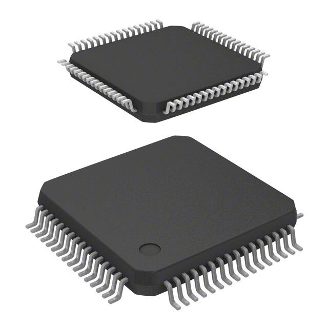
C.1 100-Pin LQFP Mechanical Dimensions . . . . . . . . . . . . . . . . . . . . . . . . . . . . . . . . . . . . . . . . . . . . 757
MC9S12HY/HA-Family Reference Manual, Rev. 1.05
Freescale Semiconductor
9
�C.2 64-Pin LQFP Mechanical Dimensions . . . . . . . . . . . . . . . . . . . . . . . . . . . . . . . . . . . . . . . . . . . . . 760
Appendix D
PCB Layout Guidelines
Appendix E
Derivative Differences
E.1
Memory Sizes and Package Options S12HY/S12HA - Family . . . . . . . . . . . . . . . . . . . . . . . . . . 767
Appendix F
Detailed Register Address Map
MC9S12HY/HA-Family Reference Manual, Rev. 1.05
10
Freescale Semiconductor
�Chapter 1
Device Overview MC9S12HY/HA-Family
1.1
Introduction
The MC9S12HY/HA family is an automotive, 16-bit microcontroller product line that is specifically
designed for entry level instrument clusters. This family also services generic automotive applications
requiring CAN, LCD, Motor driver control or LIN/J2602. Typical examples of these applications include
instrument clusters for automobiles and 2 or 3 wheelers, HVAC displays, general purpose motor control
and body controllers.
The MC9S12HY/HA family uses many of the same features found on the MC9S12P family, including
error correction code (ECC) on flash memory, a separate data-flash module for diagnostic or data storage,
a fast analog-to-digital converter (ATD) and a frequency modulated phase locked loop (IPLL) that
improves the EMC performance. The MC9S12HY/HA family features a 40x4 liquid crystal display (LCD)
controller/driver and a motor pulse width modulator (MC) consisting of up to 16 high current outputs. It
is capable of stepper motor stall detection (SSD), please contact a Freescale sales office for detailed
information.
The MC9S12HY/HA family delivers all the advantages and efficiencies of a 16-bit MCU while retaining
the low cost, power consumption, EMC, and code-size efficiency advantages currently enjoyed by users
of Freescale’s existing 8-bit and 16-bit MCU families. Like the MC9S12HZ family, the MC9S12HY/HA
family run 16-bit wide accesses without wait states for all peripherals and memories. The MC9S12HY/HA
family is available in 100-pin LQFP and 64-pin LQFP package options. In addition to the I/O ports
available in each module, further I/O ports are available with interrupt capability allowing wake-up from
stop or wait modes.
1.2
Features
This section describes the key features of the MC9S12HY/HA family.
MC9S12HY/HA-Family Reference Manual, Rev. 1.05
Freescale Semiconductor
11
�Device Overview MC9S12HY/HA-Family
1.2.1
MC9S12HY/HA Family Comparison
Table 1 provides a summary of different members of the MC9S12HY/HA family and their proposed
features. This information is intended to provide an understanding of the range of functionality offered by
this microcontroller family.
Table 1. MC9S12HY/MC9S12HA Family
Feature
MC9S12
HY32
MC9S12
HY48
MC9S12
HY64
CPU
MC9S12
HA48
MC9S12
HA64
32 KB
48 KB
64 KB
2 KB
4 KB
4 KB
HCS12 V1
Flash memory
(ECC)
32 KB
48 KB
64 KB
Data flash (ECC)
4 KB
RAM
Pin Quantity
MC9S12
HA32
2 KB
64
4 KB
100
64
CAN
4 KB
100
64
100
64
SPI
1
IIC
1
Timer 0
8 ch x 16-bit
Timer 1
8 ch x 16-bit
PWM
LCD Driver
(FPxBP)
Key Wakeup Pins
100
6 ch
8 ch
6 ch
8 ch
6 ch
8 ch
6 ch
8 ch
6 ch
8 ch
6 ch
8 ch
3
4
3
4
3
4
3
4
3
4
3
4
20x4
40x4
20x4
40x4
20x4
40x4
20x4
40x4
20x4
40x4
20x4
40x4
18
22
18
22
18
22
18
22
18
22
18
22
Yes
External osc
(4–16 MHz Pierce
with loop control)
Yes
Internal 1 MHz RC
osc
Yes
RTI, LVI, CPMU,
RST, COP, DBG,
POR, API
64
8 ch x 8-bit or 4 ch x16-bit
Frequency Modulated PLL
Supply voltage
100
-
1
Stepper Motor
Controller(1)
64
1
SCI
ADC (10-bit)
100
4.5 V – 5.5 V
Yes
1. the third stepper motor controller (M2) has a restricted output current on the 64 pin version, which is half of normal motor
pad driving current
MC9S12HY/HA-Family Reference Manual, Rev. 1.05
12
Freescale Semiconductor
�Device Overview MC9S12HY/HA-Family
1.2.2
Chip-Level Features
On-chip modules available within the family include the following features:
• S12 CPU core
• Maximum 64 MHz core freqency, 32 MHz bus frequency
• Up to 64 KB on-chip flash with ECC
• 4 KB data flash with ECC
• Up to 4 KB on-chip SRAM
• Phase locked loop (IPLL) frequency multiplier with internal filter
• 4–16 MHz amplitude controlled Pierce oscillator
• 1 MHz internal RC oscillator
• Two timer modules (TIM0 and TIM1) supporting input/output channels that provide a range of 16bit input capture, output compare, counter and pulse accumulator functions
• Pulse width modulation (PWM) module with up to 8 x 8-bit channels
• Up to 8-channel, 10-bit resolution successive approximation analog-to-digital converter (ATD)
• Up to 40x4 LCD driver
• PWM motor controller (MC) with up to 16 high current drivers
• Output slew rate control on Motor driver pad
• One serial peripheral interface (SPI) module
• One Inter-IC bus interface (IIC) module
• One serial communication interface (SCI) module supporting LIN communications
• One multi-scalable controller area network (MSCAN) module (supporting CAN protocol 2.0A/B)
• On-chip voltage regulator (VREG) for regulation of input supply and all internal voltages
• Autonomous periodic interrupt (API)
• Up to 22 key wakeup inputs
1.3
Module Features
The following sections provide more details of the modules implemented on the MC9S12HY/HA family.
1.3.1
S12 16-Bit Central Processor Unit (CPU)
The S12 CPU is a high-speed, 16-bit processing unit that has a programming model identical to that of the
industry standard M68HC11 central processor unit (CPU).
• Full 16-bit data paths support efficient arithmetic operation and high-speed math execution
• Supports instructions with odd byte counts, including many single-byte instructions. This allows
much more efficient use of ROM space.
• Extensive set of indexed addressing capabilities, including:
— Using the stack pointer as an indexing register in all indexed operations
— Using the program counter as an indexing register in all but auto increment/decrement mode
MC9S12HY/HA-Family Reference Manual, Rev. 1.05
Freescale Semiconductor
13
�Device Overview MC9S12HY/HA-Family
— Accumulator offsets using A, B, or D accumulators
— Automatic index predecrement, preincrement, postdecrement, and postincrement (by –8 to +8)
1.3.2
On-Chip Flash with ECC
On-chip flash memory on the MC9S12HY/HA features the following:
• Up to 64 KB of program flash memory
— 32 data bits plus 7 syndrome ECC (error correction code) bits allow single bit error correction
and double fault detection
— Erase sector size 512 bytes
— Automated program and erase algorithm
— User margin level setting for reads
— Protection scheme to prevent accidental program or erase
• 4 KB data flash space
— 16 data bits plus 6 syndrome ECC (error correction code) bits allow single bit error correction
and double fault detection
— Erase sector size 256 bytes
— Automated program and erase algorithm
— User margin level setting for reads
1.3.3
•
1.3.4
•
1.3.5
•
On-Chip SRAM
Up to 4 KB of general-purpose RAM, no single cycle misaligned access
Main External Oscillator (XOSC)
Loop control Pierce oscillator using a 4 MHz to 16 MHz crystal
— Current gain control on amplitude output
— Signal with low harmonic distortion
— Low power
— Good noise immunity
— Eliminates need for external current limiting resistor
— Transconductance sized for optimum start-up margin for typical crystals
Internal RC Oscillator (IRC)
Trimmable internal reference clock.
— Frequency: 1 MHz
— Trimmed accuracy over –40˚C to +125˚C ambient temperature range: ±2.0%
— Trimmed accuracy over –40˚C to +85˚C ambient temperature range: ±1.5%
MC9S12HY/HA-Family Reference Manual, Rev. 1.05
14
Freescale Semiconductor
�Device Overview MC9S12HY/HA-Family
1.3.6
•
1.3.7
•
•
•
•
•
•
•
•
1.3.8
•
•
•
•
1.3.9
•
•
•
•
Internal Phase-Locked Loop (IPLL)
Phase-locked-loop clock frequency multiplier
— No external components required
— Reference divider and multiplier allow large variety of clock rates
— Automatic bandwidth control mode for low-jitter operation
— Automatic frequency lock detector
— Configurable option to spread spectrum for reduced EMC radiation (frequency modulation)
— Reference clock sources:
– External 4–16 MHz resonator/crystal (XOSC)
– Internal 1 MHz RC oscillator (IRC)
System Integrity Support
Power-on reset (POR)
System reset generation
Illegal address detection with reset
Low-voltage detection with interrupt or reset
Real time interrupt (RTI)
Computer operating properly (COP) watchdog
— Configurable as window COP for enhanced failure detection
— Initialized out of reset using option bits located in flash memory
Clock monitor supervising the correct function of the oscillator
Temperature sensor
Timer (TIM0)
8 x 16-bit channels for input capture
8 x 16-bit channels for output compare
16-bit free-running counter with 7-bit precision prescaler
1 x 16-bit pulse accumulator
Timer (TIM1)
8 x 16-bit channels for input capture
8 x 16-bit channels for output compare
16-bit free-running counter with 7-bit precision prescaler
1 x 16-bit pulse accumulator
MC9S12HY/HA-Family Reference Manual, Rev. 1.05
Freescale Semiconductor
15
�Device Overview MC9S12HY/HA-Family
1.3.10
•
•
•
Configurable for up to 40 frontplanes and 4 backplanes or general-purpose input or output
5 modes of operation allow for different display sizes to meet application requirements
Unused frontplane and backplane pins can be used as general-purpose I/O
1.3.11
•
•
•
•
•
•
•
•
•
Inter-IC Bus Module (IIC)
1 Inter-IC (IIC) bus module
— Multi-master operation
— Soft programming for one of 256 different serial clock frequencies
— General Call (Broadcast) mode support
— 10-bit address support
1.3.14
•
Pulse Width Modulation Module (PWM)
8 channel x 8-bit or 4 channel x 16-bit pulse width modulator
— Programmable period and duty cycle per channel
— Center-aligned or left-aligned outputs
— Programmable clock select logic with a wide range of frequencies
1.3.13
•
Motor Controller (MC)
PWM motor controller (MC) with up to 16 high current drivers
Each PWM channel switchable between two drivers in an H-bridge configuration
Left, right and center aligned outputs
Support for sine and cosine drive
Dithering
Output slew rate control
1.3.12
•
Liquid Crystal Display Driver (LCD)
Controller Area Network Module (MSCAN)
1 Mbit per second, CAN 2.0 A, B software compatible
— Standard and extended data frames
— 0–8 bytes data length
— Programmable bit rate up to 1 Mbps
Five receive buffers with FIFO storage scheme
Three transmit buffers with internal prioritization
Flexible identifier acceptance filter programmable as:
— 2 x 32-bit
— 4 x 16-bit
MC9S12HY/HA-Family Reference Manual, Rev. 1.05
16
Freescale Semiconductor
�Device Overview MC9S12HY/HA-Family
•
•
•
•
•
— 8 x 8-bit
Wakeup with integrated low pass filter option
Loop back for self test
Listen-only mode to monitor CAN bus
Bus-off recovery by software intervention or automatically
16-bit time stamp of transmitted/received messages
1.3.15
•
•
•
•
•
•
•
•
Full-duplex or single-wire operation
Standard mark/space non-return-to-zero (NRZ) format
Selectable IrDA 1.4 return-to-zero-inverted (RZI) format with programmable pulse widths
13-bit baud rate selection
Programmable character length
Programmable polarity for transmitter and receiver
Active edge receive wakeup
Break detect and transmit collision detect supporting LIN
1.3.16
•
•
•
•
•
•
•
Serial Peripheral Interface Module (SPI)
Configurable 8- or 16-bit data size
Full-duplex or single-wire bidirectional
Double-buffered transmit and receive
Master or slave mode
MSB-first or LSB-first shifting
Serial clock phase and polarity options
1.3.17
•
Serial Communication Interface Module (SCI)
Analog-to-Digital Converter Module (ATD)
Up to 8-channel, 10-bit analog-to-digital converter
— 3 µs single conversion time
— 8-/10 bit resolution
— Left or right justified result data
— Internal oscillator for conversion in stop modes
— Wakeup from low power modes on analog comparison > or CompB_Addr)
In the Outside Range comparator mode, comparator pair A and B can be configured for range comparisons.
A single match condition on either of the comparators is recognized as valid. An aligned word access
which straddles the range boundary is valid only if the aligned address is outside the range.
Outside range mode in combination with tagging can be used to detect if the opcode fetches are from an
unexpected range. In forced match mode the outside range match would typically be activated at any
interrupt vector fetch or register access. This can be avoided by setting the upper range limit to $3FFFF or
lower range limit to $00000 respectively.
6.4.3
Match Modes (Forced or Tagged)
Match modes are used as qualifiers for a state sequencer change of state. The Comparator control register
TAG bits select the match mode. The modes are described in the following sections.
6.4.3.1
Forced Match
When configured for forced matching, a comparator channel match can immediately initiate a transition
to the next state sequencer state whereby the corresponding flags in DBGSR are set. The state control
register for the current state determines the next state. Forced matches are typically generated 2-3 bus
cycles after the final matching address bus cycle, independent of comparator RWE/RW settings.
Furthermore since opcode fetches occur several cycles before the opcode execution a forced match of an
opcode address typically precedes a tagged match at the same address.
6.4.3.2
Tagged Match
If a CPU taghit occurs a transition to another state sequencer state is initiated and the corresponding
DBGSR flags are set. For a comparator related taghit to occur, the DBG must first attach tags to
instructions as they are fetched from memory. When the tagged instruction reaches the execution stage of
the instruction queue a taghit is generated by the CPU. This can initiate a state sequencer transition.
6.4.3.3
Immediate Trigger
Independent of comparator matches it is possible to initiate a tracing session and/or breakpoint by writing
to the TRIG bit in DBGC1. If configured for begin aligned tracing, this triggers the state sequencer into
the Final State, if configured for end alignment, setting the TRIG bit disarms the module, ending the
session and issues a forced breakpoint request to the CPU.
It is possible to set both TRIG and ARM simultaneously to generate an immediate trigger, independent of
the current state of ARM.
MC9S12HY/HA-Family Reference Manual, Rev. 1.05
Freescale Semiconductor
209
�S12S Debug Module (S12SDBGV2)
6.4.3.4
Channel Priorities
In case of simultaneous matches the priority is resolved according to Table 6-36. The lower priority is
suppressed. It is thus possible to miss a lower priority match if it occurs simultaneously with a higher
priority. The priorities described in Table 6-36 dictate that in the case of simultaneous matches, the match
pointing to final state has highest priority followed by the lower channel number (0,1,2).
Table 6-36. Channel Priorities
Priority
Source
Highest
Lowest
6.4.4
Action
TRIG
Enter Final State
Channel pointing to Final State
Transition to next state as defined by state control registers
Match0 (force or tag hit)
Transition to next state as defined by state control registers
Match1 (force or tag hit)
Transition to next state as defined by state control registers
Match2 (force or tag hit)
Transition to next state as defined by state control registers
State Sequence Control
ARM = 0
State 0
(Disarmed)
ARM = 1
State1
State2
ARM = 0
Session Complete
(Disarm)
Final State
State3
ARM = 0
Figure 6-24. State Sequencer Diagram
The state sequencer allows a defined sequence of events to provide a trigger point for tracing of data in the
trace buffer. Once the DBG module has been armed by setting the ARM bit in the DBGC1 register, then
state1 of the state sequencer is entered. Further transitions between the states are then controlled by the
state control registers and channel matches. From Final State the only permitted transition is back to the
disarmed state0. Transition between any of the states 1 to 3 is not restricted. Each transition updates the
SSF[2:0] flags in DBGSR accordingly to indicate the current state.
Alternatively writing to the TRIG bit in DBGSC1, provides an immediate trigger independent of
comparator matches.
Independent of the state sequencer, each comparator channel can be individually configured to generate an
immediate breakpoint when a match occurs through the use of the BRK bits in the DBGxCTL registers.
Thus it is possible to generate an immediate breakpoint on selected channels, whilst a state sequencer
transition can be initiated by a match on other channels. If a debug session is ended by a match on a channel
the state sequencer transitions through Final State for a clock cycle to state0. This is independent of tracing
MC9S12HY/HA-Family Reference Manual, Rev. 1.05
210
Freescale Semiconductor
�S12S Debug Module (S12SDBGV2)
and breakpoint activity, thus with tracing and breakpoints disabled, the state sequencer enters state0 and
the debug module is disarmed.
6.4.4.1
Final State
On entering Final State a trigger may be issued to the trace buffer according to the trace alignment control
as defined by the TALIGN bit (see 6.3.2.3, "Debug Trace Control Register (DBGTCR)"”). If the
TSOURCE bit in DBGTCR is clear then the trace buffer is disabled and the transition to Final State can
only generate a breakpoint request. In this case or upon completion of a tracing session when tracing is
enabled, the ARM bit in the DBGC1 register is cleared, returning the module to the disarmed state0. If
tracing is enabled a breakpoint request can occur at the end of the tracing session. If neither tracing nor
breakpoints are enabled then when the final state is reached it returns automatically to state0 and the debug
module is disarmed.
6.4.5
Trace Buffer Operation
The trace buffer is a 64 lines deep by 20-bits wide RAM array. The DBG module stores trace information
in the RAM array in a circular buffer format. The system accesses the RAM array through a register
window (DBGTBH:DBGTBL) using 16-bit wide word accesses. After each complete 20-bit trace buffer
line is read, an internal pointer into the RAM increments so that the next read receives fresh information.
Data is stored in the format shown in Table 6-37 and Table 6-40. After each store the counter register
DBGCNT is incremented. Tracing of CPU activity is disabled when the BDM is active. Reading the trace
buffer whilst the DBG is armed returns invalid data and the trace buffer pointer is not incremented.
6.4.5.1
Trace Trigger Alignment
Using the TALIGN bit (see 6.3.2.3, "Debug Trace Control Register (DBGTCR)") it is possible to align the
trigger with the end or the beginning of a tracing session.
If end alignment is selected, tracing begins when the ARM bit in DBGC1 is set and State1 is entered; the
transition to Final State signals the end of the tracing session. Tracing with Begin-Trigger starts at the
opcode of the trigger. Using end alignment or when the tracing is initiated by writing to the TRIG bit whilst
configured for begin alignment, tracing starts in the second cycle after the DBGC1 write cycle.
6.4.5.1.1
Storing with Begin Trigger Alignment
Storing with begin alignment, data is not stored in the Trace Buffer until the Final State is entered. Once
the trigger condition is met the DBG module remains armed until 64 lines are stored in the Trace Buffer.
If the trigger is at the address of the change-of-flow instruction the change of flow associated with the
trigger is stored in the Trace Buffer. Using begin alignment together with tagging, if the tagged instruction
is about to be executed then the trace is started. Upon completion of the tracing session the breakpoint is
generated, thus the breakpoint does not occur at the tagged instruction boundary.
6.4.5.1.2
Storing with End Trigger Alignment
Storing with end alignment, data is stored in the Trace Buffer until the Final State is entered, at which point
the DBG module becomes disarmed and no more data is stored. If the trigger is at the address of a change
MC9S12HY/HA-Family Reference Manual, Rev. 1.05
Freescale Semiconductor
211
�S12S Debug Module (S12SDBGV2)
of flow instruction, the trigger event is not stored in the Trace Buffer. If all trace buffer lines have been
used before a trigger event occurrs then the trace continues at the first line, overwriting the oldest entries.
6.4.5.2
Trace Modes
Four trace modes are available. The mode is selected using the TRCMOD bits in the DBGTCR register.
Tracing is enabled using the TSOURCE bit in the DBGTCR register. The modes are described in the
following subsections.
6.4.5.2.1
Normal Mode
In Normal Mode, change of flow (COF) program counter (PC) addresses are stored.
COF addresses are defined as follows:
• Source address of taken conditional branches (long, short, bit-conditional, and loop primitives)
• Destination address of indexed JMP, JSR, and CALL instruction
• Destination address of RTI, RTS, and RTC instructions
• Vector address of interrupts, except for BDM vectors
LBRA, BRA, BSR, BGND as well as non-indexed JMP, JSR, and CALL instructions are not classified as
change of flow and are not stored in the trace buffer.
Stored information includes the full 18-bit address bus and information bits, which contains a
source/destination bit to indicate whether the stored address was a source address or destination address.
NOTE
When a COF instruction with destination address is executed, the
destination address is stored to the trace buffer on instruction completion,
indicating the COF has taken place. If an interrupt occurs simultaneously
then the next instruction carried out is actually from the interrupt service
routine. The instruction at the destination address of the original program
flow gets executed after the interrupt service routine.
In the following example an IRQ interrupt occurs during execution of the
indexed JMP at address MARK1. The BRN at the destination (SUB_1) is
not executed until after the IRQ service routine but the destination address
is entered into the trace buffer to indicate that the indexed JMP COF has
taken place.
MARK1
MARK2
LDX
JMP
NOP
#SUB_1
0,X
SUB_1
BRN
*
ADDR1
NOP
DBNE
A,PART5
LDAB
STAB
#$F0
VAR_C1
IRQ_ISR
; IRQ interrupt occurs during execution of this
;
; JMP Destination address TRACE BUFFER ENTRY 1
; RTI Destination address TRACE BUFFER ENTRY 3
;
; Source address TRACE BUFFER ENTRY 4
; IRQ Vector $FFF2 = TRACE BUFFER ENTRY 2
MC9S12HY/HA-Family Reference Manual, Rev. 1.05
212
Freescale Semiconductor
�S12S Debug Module (S12SDBGV2)
RTI
;
The execution flow taking into account the IRQ is as follows
MARK1
IRQ_ISR
SUB_1
ADDR1
6.4.5.2.2
LDX
JMP
LDAB
STAB
RTI
BRN
NOP
DBNE
#SUB_1
0,X
#$F0
VAR_C1
;
;
;
*
A,PART5
;
;
Loop1 Mode
Loop1 Mode, similarly to Normal Mode also stores only COF address information to the trace buffer, it
however allows the filtering out of redundant information.
The intent of Loop1 Mode is to prevent the Trace Buffer from being filled entirely with duplicate
information from a looping construct such as delays using the DBNE instruction or polling loops using
BRSET/BRCLR instructions. Immediately after address information is placed in the Trace Buffer, the
DBG module writes this value into a background register. This prevents consecutive duplicate address
entries in the Trace Buffer resulting from repeated branches.
Loop1 Mode only inhibits consecutive duplicate source address entries that would typically be stored in
most tight looping constructs. It does not inhibit repeated entries of destination addresses or vector
addresses, since repeated entries of these would most likely indicate a bug in the user’s code that the DBG
module is designed to help find.
6.4.5.2.3
Detail Mode
In Detail Mode, address and data for all memory and register accesses is stored in the trace buffer. This
mode is intended to supply additional information on indexed, indirect addressing modes where storing
only the destination address would not provide all information required for a user to determine where the
code is in error. This mode also features information bit storage to the trace buffer, for each address byte
storage. The information bits indicate the size of access (word or byte) and the type of access (read or
write).
When tracing in Detail Mode, all cycles are traced except those when the CPU is either in a free or opcode
fetch cycle.
6.4.5.2.4
Compressed Pure PC Mode
In Compressed Pure PC Mode, the PC addresses of all executed opcodes, including illegal opcodes are
stored. A compressed storage format is used to increase the effective depth of the trace buffer. This is
achieved by storing the lower order bits each time and using 2 information bits to indicate if a 64 byte
boundary has been crossed, in which case the full PC is stored.
Each Trace Buffer row consists of 2 information bits and 18 PC address bits
MC9S12HY/HA-Family Reference Manual, Rev. 1.05
Freescale Semiconductor
213
�S12S Debug Module (S12SDBGV2)
NOTE:
When tracing is terminated using forced breakpoints, latency in breakpoint
generation means that opcodes following the opcode causing the breakpoint
can be stored to the trace buffer. The number of opcodes is dependent on
program flow. This can be avoided by using tagged breakpoints.
6.4.5.3
Trace Buffer Organization (Normal, Loop1, Detail modes)
ADRH, ADRM, ADRL denote address high, middle and low byte respectively. The numerical suffix refers
to the tracing count. The information format for Loop1 and Normal modes is identical. In Detail mode, the
address and data for each entry are stored on consecutive lines, thus the maximum number of entries is 32.
In this case DBGCNT bits are incremented twice, once for the address line and once for the data line, on
each trace buffer entry. In Detail mode CINF comprises of R/W and size access information (CRW and
CSZ respectively).
Single byte data accesses in Detail Mode are always stored to the low byte of the trace buffer (DATAL)
and the high byte is cleared. When tracing word accesses, the byte at the lower address is always stored to
trace buffer byte1 and the byte at the higher address is stored to byte0.
Table 6-37. Trace Buffer Organization (Normal,Loop1,Detail modes)
Entry 1
8-bits
8-bits
Field 2
Field 1
Field 0
CINF1,ADRH1
ADRM1
ADRL1
0
DATAH1
DATAL1
CINF2,ADRH2
ADRM2
ADRL2
0
DATAH2
DATAL2
Entry 1
PCH1
PCM1
PCL1
Entry 2
PCH2
PCM2
PCL2
Detail Mode
Entry 2
Normal/Loop1
Modes
6.4.5.3.1
4-bits
Entry
Number
Mode
Information Bit Organization
The format of the bits is dependent upon the active trace mode as described below.
Field2 Bits in Detail Mode
Bit 3
Bit 2
CSZ
CRW
Bit 1
Bit 0
ADDR[17] ADDR[16]
Figure 6-25. Field2 Bits in Detail Mode
In Detail Mode the CSZ and CRW bits indicate the type of access being made by the CPU.
MC9S12HY/HA-Family Reference Manual, Rev. 1.05
214
Freescale Semiconductor
�S12S Debug Module (S12SDBGV2)
Table 6-38. Field Descriptions
Bit
Description
3
CSZ
Access Type Indicator— This bit indicates if the access was a byte or word size when tracing in Detail Mode
0 Word Access
1 Byte Access
2
CRW
Read Write Indicator — This bit indicates if the corresponding stored address corresponds to a read or write
access when tracing in Detail Mode.
0 Write Access
1 Read Access
1
ADDR[17]
Address Bus bit 17— Corresponds to system address bus bit 17.
0
ADDR[16]
Address Bus bit 16— Corresponds to system address bus bit 16.
Field2 Bits in Normal and Loop1 Modes
Bit 3
Bit 2
Bit 1
Bit 0
CSD
CVA
PC17
PC16
Figure 6-26. Information Bits PCH
Table 6-39. PCH Field Descriptions
Bit
Description
3
CSD
Source Destination Indicator — In Normal and Loop1 mode this bit indicates if the corresponding stored
address is a source or destination address. This bit has no meaning in Compressed Pure PC mode.
0 Source Address
1 Destination Address
2
CVA
Vector Indicator — In Normal and Loop1 mode this bit indicates if the corresponding stored address is a vector
address. Vector addresses are destination addresses, thus if CVA is set, then the corresponding CSD is also set.
This bit has no meaning in Compressed Pure PC mode.
0 Non-Vector Destination Address
1 Vector Destination Address
1
PC17
Program Counter bit 17— In Normal and Loop1 mode this bit corresponds to program counter bit 17.
0
PC16
Program Counter bit 16— In Normal and Loop1 mode this bit corresponds to program counter bit 16.
6.4.5.4
Trace Buffer Organization (Compressed Pure PC mode)
Table 6-40. Trace Buffer Organization Example (Compressed PurePC mode)
Mode
2-bits
Line
Number Field 3
6-bits
6-bits
6-bits
Field 2
Field 1
Field 0
MC9S12HY/HA-Family Reference Manual, Rev. 1.05
Freescale Semiconductor
215
�S12S Debug Module (S12SDBGV2)
Compressed
Pure PC Mode
Line 1
00
Line 2
11
PC4
PC1 (Initial 18-bit PC Base Address)
PC3
PC2
Line 3
01
0
0
PC5
Line 4
00
Line 5
10
Line 6
00
PC6 (New 18-bit PC Base Address)
0
PC8
PC7
PC9 (New 18-bit PC Base Address)
NOTE
Configured for end aligned triggering in compressed PurePC mode, then
after rollover it is possible that the oldest base address is overwritten. In this
case all entries between the pointer and the next base address have lost their
base address following rollover. For example in Table 6-40 if one line of
rollover has occurred, Line 1, PC1, is overwritten with a new entry. Thus the
entries on Lines 2 and 3 have lost their base address. For reconstruction of
program flow the first base address following the pointer must be used, in
the example, Line 4. The pointer points to the oldest entry, Line 2.
Field3 Bits in Compressed Pure PC Modes
Table 6-41. Compressed Pure PC Mode Field 3 Information Bit Encoding
INF1
INF0
TRACE BUFFER ROW CONTENT
0
0
Base PC address TB[17:0] contains a full PC[17:0] value
0
1
Trace Buffer[5:0] contain incremental PC relative to base address zero value
1
0
Trace Buffer[11:0] contain next 2 incremental PCs relative to base address zero value
1
1
Trace Buffer[17:0] contain next 3 incremental PCs relative to base address zero value
Each time that PC[17:6] differs from the previous base PC[17:6], then a new base address is stored. The
base address zero value is the lowest address in the 64 address range
The first line of the trace buffer always gets a base PC address, this applies also on rollover.
6.4.5.5
Reading Data from Trace Buffer
The data stored in the Trace Buffer can be read provided the DBG module is not armed, is configured for
tracing (TSOURCE bit is set) and the system not secured. When the ARM bit is written to 1 the trace buffer
is locked to prevent reading. The trace buffer can only be unlocked for reading by a single aligned word
write to DBGTB when the module is disarmed.
The Trace Buffer can only be read through the DBGTB register using aligned word reads, any byte or
misaligned reads return 0 and do not cause the trace buffer pointer to increment to the next trace buffer
address. The Trace Buffer data is read out first-in first-out. By reading CNT in DBGCNT the number of
valid lines can be determined. DBGCNT does not decrement as data is read.
Whilst reading an internal pointer is used to determine the next line to be read. After a tracing session, the
pointer points to the oldest data entry, thus if no rollover has occurred, the pointer points to line0, otherwise
it points to the line with the oldest entry. In compressed Pure PC mode on rollover the line with the oldest
MC9S12HY/HA-Family Reference Manual, Rev. 1.05
216
Freescale Semiconductor
�S12S Debug Module (S12SDBGV2)
data entry may also contain newer data entries in fields 0 and 1. Thus if rollover is indicated by the TBF
bit, the line status must be decoded using the INF bits in field3 of that line. If both INF bits are clear then
the line contains only entries from before the last rollover.
If INF0=1 then field 0 contains post rollover data but fields 1 and 2 contain pre rollover data.
If INF1=1 then fields 0 and 1 contain post rollover data but field 2 contains pre rollover data.
The pointer is initialized by each aligned write to DBGTBH to point to the oldest data again. This enables
an interrupted trace buffer read sequence to be easily restarted from the oldest data entry.
The least significant word of line is read out first. This corresponds to the fields 1 and 0 of Table 6-37. The
next word read returns field 2 in the least significant bits [3:0] and “0” for bits [15:4].
Reading the Trace Buffer while the DBG module is armed returns invalid data and no shifting of the RAM
pointer occurs.
6.4.5.6
Trace Buffer Reset State
The Trace Buffer contents and DBGCNT bits are not initialized by a system reset. Thus should a system
reset occur, the trace session information from immediately before the reset occurred can be read out and
the number of valid lines in the trace buffer is indicated by DBGCNT. The internal pointer to the current
trace buffer address is initialized by unlocking the trace buffer and points to the oldest valid data even if a
reset occurred during the tracing session. To read the trace buffer after a reset, TSOURCE must be set,
otherwise the trace buffer reads as all zeroes. Generally debugging occurrences of system resets is best
handled using end trigger alignment since the reset may occur before the trace trigger, which in the begin
trigger alignment case means no information would be stored in the trace buffer.
The Trace Buffer contents and DBGCNT bits are undefined following a POR.
NOTE
An external pin RESET that occurs simultaneous to a trace buffer entry can,
in very seldom cases, lead to either that entry being corrupted or the first
entry of the session being corrupted. In such cases the other contents of the
trace buffer still contain valid tracing information. The case occurs when the
reset assertion coincides with the trace buffer entry clock edge.
6.4.6
Tagging
A tag follows program information as it advances through the instruction queue. When a tagged instruction
reaches the head of the queue a tag hit occurs and can initiate a state sequencer transition.
Each comparator control register features a TAG bit, which controls whether the comparator match causes
a state sequencer transition immediately or tags the opcode at the matched address. If a comparator is
enabled for tagged comparisons, the address stored in the comparator match address registers must be an
opcode address.
Using Begin trigger together with tagging, if the tagged instruction is about to be executed then the
transition to the next state sequencer state occurs. If the transition is to the Final State, tracing is started.
Only upon completion of the tracing session can a breakpoint be generated. Using End alignment, when
MC9S12HY/HA-Family Reference Manual, Rev. 1.05
Freescale Semiconductor
217
�S12S Debug Module (S12SDBGV2)
the tagged instruction is about to be executed and the next transition is to Final State then a breakpoint is
generated immediately, before the tagged instruction is carried out.
R/W monitoring, access size (SZ) monitoring and data bus monitoring are not useful if tagging is selected,
since the tag is attached to the opcode at the matched address and is not dependent on the data bus nor on
the type of access. Thus these bits are ignored if tagging is selected.
When configured for range comparisons and tagging, the ranges are accurate only to word boundaries.
Tagging is disabled when the BDM becomes active.
6.4.7
Breakpoints
It is possible to generate breakpoints from channel transitions to final state or using software to write to
the TRIG bit in the DBGC1 register.
6.4.7.1
Breakpoints From Comparator Channels
Breakpoints can be generated when the state sequencer transitions to the Final State. If configured for
tagging, then the breakpoint is generated when the tagged opcode reaches the execution stage of the
instruction queue.
If a tracing session is selected by the TSOURCE bit, breakpoints are requested when the tracing session
has completed, thus if Begin aligned triggering is selected, the breakpoint is requested only on completion
of the subsequent trace (see Table 6-42). If no tracing session is selected, breakpoints are requested
immediately.
If the BRK bit is set, then the associated breakpoint is generated immediately independent of tracing
trigger alignment.
Table 6-42. Breakpoint Setup For CPU Breakpoints
BRK
TALIGN
DBGBRK
0
0
0
Fill Trace Buffer until trigger then disarm (no breakpoints)
0
0
1
Fill Trace Buffer until trigger, then breakpoint request occurs
0
1
0
Start Trace Buffer at trigger (no breakpoints)
0
1
1
Start Trace Buffer at trigger
A breakpoint request occurs when Trace Buffer is full
1
x
1
Terminate tracing and generate breakpoint immediately on trigger
1
x
0
Terminate tracing immediately on trigger
6.4.7.2
Breakpoint Alignment
Breakpoints Generated Via The TRIG Bit
If a TRIG triggers occur, the Final State is entered whereby tracing trigger alignment is defined by the
TALIGN bit. If a tracing session is selected by the TSOURCE bit, breakpoints are requested when the
tracing session has completed, thus if Begin aligned triggering is selected, the breakpoint is requested only
on completion of the subsequent trace (see Table 6-42). If no tracing session is selected, breakpoints are
MC9S12HY/HA-Family Reference Manual, Rev. 1.05
218
Freescale Semiconductor
�S12S Debug Module (S12SDBGV2)
requested immediately. TRIG breakpoints are possible with a single write to DBGC1, setting ARM and
TRIG simultaneously.
6.4.7.3
Breakpoint Priorities
If a TRIG trigger occurs after Begin aligned tracing has already started, then the TRIG no longer has an
effect. When the associated tracing session is complete, the breakpoint occurs. Similarly if a TRIG is
followed by a subsequent comparator channel match, it has no effect, since tracing has already started.
If a forced SWI breakpoint coincides with a BGND in user code with BDM enabled, then the BDM is
activated by the BGND and the breakpoint to SWI is suppressed.
6.4.7.3.1
DBG Breakpoint Priorities And BDM Interfacing
Breakpoint operation is dependent on the state of the BDM module. If the BDM module is active, the CPU
is executing out of BDM firmware, thus comparator matches and associated breakpoints are disabled. In
addition, while executing a BDM TRACE command, tagging into BDM is disabled. If BDM is not active,
the breakpoint gives priority to BDM requests over SWI requests if the breakpoint happens to coincide
with a SWI instruction in user code. On returning from BDM, the SWI from user code gets executed.
Table 6-43. Breakpoint Mapping Summary
DBGBRK
BDM Bit
(DBGC1[4])
BDM
Enabled
BDM
Active
Breakpoint
Mapping
0
X
X
X
No Breakpoint
1
0
X
0
Breakpoint to SWI
X
X
1
1
No Breakpoint
1
1
0
X
Breakpoint to SWI
1
1
1
0
Breakpoint to BDM
BDM cannot be entered from a breakpoint unless the ENABLE bit is set in the BDM. If entry to BDM via
a BGND instruction is attempted and the ENABLE bit in the BDM is cleared, the CPU actually executes
the BDM firmware code, checks the ENABLE and returns if ENABLE is not set. If not serviced by the
monitor then the breakpoint is re-asserted when the BDM returns to normal CPU flow.
If the comparator register contents coincide with the SWI/BDM vector address then an SWI in user code
could coincide with a DBG breakpoint. The CPU ensures that BDM requests have a higher priority than
SWI requests. Returning from the BDM/SWI service routine care must be taken to avoid a repeated
breakpoint at the same address.
Should a tagged or forced breakpoint coincide with a BGND in user code, then the instruction that follows
the BGND instruction is the first instruction executed when normal program execution resumes.
MC9S12HY/HA-Family Reference Manual, Rev. 1.05
Freescale Semiconductor
219
�S12S Debug Module (S12SDBGV2)
NOTE
When program control returns from a tagged breakpoint using an RTI or
BDM GO command without program counter modification it returns to the
instruction whose tag generated the breakpoint. To avoid a repeated
breakpoint at the same location reconfigure the DBG module in the SWI
routine, if configured for an SWI breakpoint, or over the BDM interface by
executing a TRACE command before the GO to increment the program flow
past the tagged instruction.
6.5
6.5.1
Application Information
State Machine scenarios
Defining the state control registers as SCR1,SCR2, SCR3 and M0,M1,M2 as matches on channels 0,1,2
respectively. SCR encoding supported by S12SDBGV1 are shown in black. SCR encoding supported only
in S12SDBGV2 are shown in red. For backwards compatibility the new scenarios use a 4th bit in each SCR
register. Thus the existing encoding for SCRx[2:0] is not changed.
6.5.2
Scenario 1
A trigger is generated if a given sequence of 3 code events is executed.
Figure 6-27. Scenario 1
SCR2=0010
SCR1=0011
State1
M1
SCR3=0111
M2
State2
State3
M0
Final State
Scenario 1 is possible with S12SDBGV1 SCR encoding
6.5.3
Scenario 2
A trigger is generated if a given sequence of 2 code events is executed.
Figure 6-28. Scenario 2a
SCR2=0101
SCR1=0011
State1
M1
State2
M2
Final State
MC9S12HY/HA-Family Reference Manual, Rev. 1.05
220
Freescale Semiconductor
�S12S Debug Module (S12SDBGV2)
A trigger is generated if a given sequence of 2 code events is executed, whereby the first event is entry into
a range (COMPA,COMPB configured for range mode). M1 is disabled in range modes.
Figure 6-29. Scenario 2b
SCR2=0101
SCR1=0111
State1
M01
M2
State2
Final State
A trigger is generated if a given sequence of 2 code events is executed, whereby the second event is entry
into a range (COMPA,COMPB configured for range mode)
Figure 6-30. Scenario 2c
SCR2=0011
SCR1=0010
State1
M2
M0
State2
Final State
All 3 scenarios 2a,2b,2c are possible with the S12SDBGV1 SCR encoding
6.5.4
Scenario 3
A trigger is generated immediately when one of up to 3 given events occurs
Figure 6-31. Scenario 3
SCR1=0000
State1
M012
Final State
Scenario 3 is possible with S12SDBGV1 SCR encoding
6.5.5
Scenario 4
Trigger if a sequence of 2 events is carried out in an incorrect order. Event A must be followed by event B
and event B must be followed by event A. 2 consecutive occurrences of event A without an intermediate
MC9S12HY/HA-Family Reference Manual, Rev. 1.05
Freescale Semiconductor
221
�S12S Debug Module (S12SDBGV2)
event B cause a trigger. Similarly 2 consecutive occurrences of event B without an intermediate event A
cause a trigger. This is possible by using CompA and CompC to match on the same address as shown.
Figure 6-32. Scenario 4a
SCR1=0100 State1
M1
SCR3=0001
State 3
M0
State2
M2
M0
M1
M1
SCR2=0011
Final State
This scenario is currently not possible using 2 comparators only. S12SDBGV2 makes it possible with 2
comparators, State 3 allowing a M0 to return to state 2, whilst a M2 leads to final state as shown.
Figure 6-33. Scenario 4b (with 2 comparators)
SCR1=0110 State1
M2
SCR3=1110
State 3
M0
State2
M0
M01
M2
M2
SCR2=1100
M1 disabled in
range mode
Final State
The advantage of using only 2 channels is that now range comparisons can be included (channel0)
This however violates the S12SDBGV1 specification, which states that a match leading to final state
always has priority in case of a simultaneous match, whilst priority is also given to the lowest channel
number. For S12SDBG the corresponding CPU priority decoder is removed to support this, such that on
simultaneous taghits, taghits pointing to final state have highest priority. If no taghit points to final state
then the lowest channel number has priority. Thus with the above encoding from State3, the CPU and DBG
would break on a simultaneous M0/M2.
MC9S12HY/HA-Family Reference Manual, Rev. 1.05
222
Freescale Semiconductor
�S12S Debug Module (S12SDBGV2)
6.5.6
Scenario 5
Trigger if following event A, event C precedes event B. i.e. the expected execution flow is A->B->C.
Figure 6-34. Scenario 5
SCR2=0110
SCR1=0011
M1
State1
M0
State2
Final State
M2
Scenario 5 is possible with the S12SDBGV1 SCR encoding
6.5.7
Scenario 6
Trigger if event A occurs twice in succession before any of 2 other events (BC) occurs. This scenario is
not possible using the S12SDBGV1 SCR encoding. S12SDBGV2 includes additions shown in red. The
change in SCR1 encoding also has the advantage that a State1->State3 transition using M0 is now possible.
This is advantageous because range and data bus comparisons use channel0 only.
Figure 6-35. Scenario 6
SCR3=1010
SCR1=1001
State1
M0
State3
M0
Final State
M12
6.5.8
Scenario 7
Trigger when a series of 3 events is executed out of order. Specifying the event order as M1,M2,M0 to run
in loops (120120120). Any deviation from that order should trigger. This scenario is not possible using the
S12SDBGV1 SCR encoding because OR possibilities are very limited in the channel encoding. By adding
OR forks as shown in red this scenario is possible.
Figure 6-36. Scenario 7
M01
SCR2=1100
SCR1=1101
State1
M1
State2
SCR3=1101
M2
State3
M12
Final State
M0
M02
MC9S12HY/HA-Family Reference Manual, Rev. 1.05
Freescale Semiconductor
223
�S12S Debug Module (S12SDBGV2)
On simultaneous matches the lowest channel number has priority so with this configuration the forking
from State1 has the peculiar effect that a simultaneous match0/match1 transitions to final state but a
simultaneous match2/match1transitions to state2.
6.5.9
Scenario 8
Trigger when a routine/event at M2 follows either M1 or M0.
Figure 6-37. Scenario 8a
SCR2=0101
SCR1=0111
M01
State1
M2
State2
Final State
Trigger when an event M2 is followed by either event M0 or event M1
Figure 6-38. Scenario 8b
SCR2=0111
SCR1=0010
State1
M2
State2
M01
Final State
Scenario 8a and 8b are possible with the S12SDBGV1 and S12SDBGV2 SCR encoding
6.5.10
Scenario 9
Trigger when a routine/event at A (M2) does not follow either B or C (M1 or M0) before they are executed
again. This cannot be realized with theS12SDBGV1 SCR encoding due to OR limitations. By changing
the SCR2 encoding as shown in red this scenario becomes possible.
Figure 6-39. Scenario 9
SCR2=1111
SCR1=0111
State1
M01
State2
M01
Final State
M2
6.5.11
Scenario 10
Trigger if an event M0 occurs following up to two successive M2 events without the resetting event M1.
As shown up to 2 consecutive M2 events are allowed, whereby a reset to State1 is possible after either one
or two M2 events. If an event M0 occurs following the second M2, before M1 resets to State1 then a trigger
MC9S12HY/HA-Family Reference Manual, Rev. 1.05
224
Freescale Semiconductor
�S12S Debug Module (S12SDBGV2)
is generated. Configuring CompA and CompC the same, it is possible to generate a breakpoint on the third
consecutive occurrence of event M0 without a reset M1.
Figure 6-40. Scenario 10a
M1
SCR1=0010
State1
M2
SCR2=0100
SCR3=0010
M2
State2
M0
State3
Final State
M1
Figure 6-41. Scenario 10b
M0
SCR2=0011
SCR1=0010
State1
M2
State2
SCR3=0000
M1
State3
Final State
M0
Scenario 10b shows the case that after M2 then M1 must occur before M0. Starting from a particular point
in code, event M2 must always be followed by M1 before M0. If after any M2, event M0 occurs before
M1 then a trigger is generated.
MC9S12HY/HA-Family Reference Manual, Rev. 1.05
Freescale Semiconductor
225
�S12S Debug Module (S12SDBGV2)
MC9S12HY/HA-Family Reference Manual, Rev. 1.05
226
Freescale Semiconductor
�Chapter 7
S12 Clock, Reset and Power Management Unit (S12CPMU)
Block Description
Revision History
Version Revision Effective
Number
Date
Date
V01.00
16 Jan.07
16 Jan. 07
Author
Description of Changes
Initial release
V01.01
9 July 08
9 July 08
added IRCLK to Block Diagram
V01.02
7 Oct. 08
7 Oct. 08
clarified and detailed oscillator filter functionality
V01.03
11 Dec. 08 11 Dec. 08
added note, that startup time of external oscillator tUPOSC must be
considered, especially when entering Pseudo Stop Mode
V01.04
17 Jun. 09 17 Jun. 09
Modified reset phase descriptions to reference fVCORST instead of
fPLLRST and correct typo of RESET pin sample point from 64 to 256
cycles in section: Description of Reset Operation
V01.05
27 Apr. 10
27 Apr. 10
Major rework fixing typos, figures and tables and improved
description of Adaptive Oscillator Filter.
V01.06
03 Mai 10
03 Mai 10
Improved pin description in Section 7.2, “Signal Description.
Improved description of bit write access conditions for CPMUCLK
register bits in Section 7.3.2.6, “S12CPMU Clock Select Register
(CPMUCLKS).
Improved description of bit write access conditions for CPMUCOP
register bits in Section 7.3.2.9, “S12CPMU COP Control Register
(CPMUCOP).
Updated bit description OSCFILT[4:0] to get one common wording
throughout the document.
Updated register description CPMUPROT to have list of protected
registers only once in the document which gets referenced.
Wording corrections throughout document.
V01.06
06 Mai 10
06 Mai 10
Changed feature name “adaptive spike filter” to “Adaptive Oscillator
Filter” in Figure 7-2.
Added a node to the description of the CPMUOSC register.
V01.07
25 July 12
25 July 12
Enhanced VSEL bit description that setting HTE bit before is
required.
MC9S12HY/HA-Family Reference Manual, Rev. 1.05
Freescale Semiconductor
227
�S12 Clock, Reset and Power Management Unit (S12CPMU) Block Description
7.1
Introduction
This specification describes the function of the Clock, Reset and Power Management Unit (S12CPMU).
• The Pierce oscillator (OSCLCP) provides a robust, low-noise and low-power external clock source.
It is designed for optimal start-up margin with typical crystal oscillators.
• The Voltage regulator (IVREG) operates from the range 3.13V to 5.5V. It provides all the required
chip internal voltages and voltage monitors.
• The Phase Locked Loop (PLL) provides a highly accurate frequency multiplier with internal filter.
• The Internal Reference Clock (IRC1M) provides a1MHz clock.
7.1.1
Features
The Pierce Oscillator (OSCLCP) contains circuitry to dynamically control current gain in the output
amplitude. This ensures a signal with low harmonic distortion, low power and good noise immunity.
• Supports crystals or resonators from 4MHz to 16MHz.
• High noise immunity due to input hysteresis and spike filtering.
• Low RF emissions with peak-to-peak swing limited dynamically
• Transconductance (gm) sized for optimum start-up margin for typical crystals
• Dynamic gain control eliminates the need for external current limiting resistor
• Integrated resistor eliminates the need for external bias resistor.
• Low power consumption: Operates from internal 1.8V (nominal) supply, Amplitude control limits
power
The Voltage Regulator (IVREG) has the following features:
• Input voltage range from 3.13V to 5.5V
• Low-voltage detect (LVD) with low-voltage interrupt (LVI)
• Power-on reset (POR)
• Low-voltage reset (LVR)
The Phase Locked Loop (PLL) has the following features:
• highly accurate and phase locked frequency multiplier
• Configurable internal filter for best stability and lock time.
• Frequency modulation for defined jitter and reduced emission
• Automatic frequency lock detector
• Interrupt request on entry or exit from locked condition
• Reference clock either external (crystal) or internal square wave (1MHz IRC1M) based.
• PLL stability is sufficient for LIN communication, even if using IRC1M as reference clock
The Internal Reference Clock (IRC1M) has the following features:
• Trimmable in frequency
• Factory trimmed value for 1MHz in Flash Memory, can be overwritten by application if required
MC9S12HY/HA-Family Reference Manual, Rev. 1.05
228
Freescale Semiconductor
�S12 Clock, Reset and Power Management Unit (S12CPMU) Block Description
Other features of the S12CPMU include
• Clock monitor to detect loss of crystal
• Autonomous periodical interrupt (API)
• Bus Clock Generator
— Clock switch to select either PLLCLK or external crystal/resonator based Bus Clock
— PLLCLK divider to adjust system speed
• System Reset generation from the following possible sources:
— Power-on reset (POR)
— Low-voltage reset (LVR)
— Illegal address access
— COP time out
— Loss of oscillation (clock monitor fail)
— External pin RESET
MC9S12HY/HA-Family Reference Manual, Rev. 1.05
Freescale Semiconductor
229
�S12 Clock, Reset and Power Management Unit (S12CPMU) Block Description
7.1.2
Modes of Operation
This subsection lists and briefly describes all operating modes supported by the S12CPMU.
7.1.2.1
Run Mode
The voltage regulator is in Full Performance Mode (FPM).
The Phase Locked Loop (PLL) is on.
The Internal Reference Clock (IRC1M) is on.
The API is available.
• PLL Engaged Internal (PEI)
— This is the default mode after System Reset and Power-On Reset.
— The Bus Clock is based on the PLLCLK.
— After reset the PLL is configured for 64MHz VCOCLK operation
Post divider is 0x03, so PLLCLK is VCOCLK divided by 4, that is 16MHz and Bus Clock is
8MHz.
The PLL can be re-configured for other bus frequencies.
— The reference clock for the PLL (REFCLK) is based on internal reference clock IRC1M
• PLL Engaged External (PEE)
— The Bus Clock is based on the PLLCLK.
— This mode can be entered from default mode PEI by performing the following steps:
– Configure the PLL for desired bus frequency.
– Program the reference divider (REFDIV[3:0] bits) to divide down oscillator frequency if
necessary.
– Enable the external oscillator (OSCE bit)
• PLL Bypassed External (PBE)
— The Bus Clock is based on the Oscillator Clock (OSCCLK).
— This mode can be entered from default mode PEI by performing the following steps:
– Enable the external oscillator (OSCE bit)
– Wait for oscillator to start up (UPOSC=1)
– Select the Oscillator Clock (OSCCLK) as Bus Clock (PLLSEL=0).
— The PLLCLK is still on to filter possible spikes of the external oscillator clock.
7.1.2.2
Wait Mode
For S12CPMU Wait Mode is the same as Run Mode.
MC9S12HY/HA-Family Reference Manual, Rev. 1.05
230
Freescale Semiconductor
�S12 Clock, Reset and Power Management Unit (S12CPMU) Block Description
7.1.2.3
Stop Mode
This mode is entered by executing the CPU STOP instruction.
The voltage regulator is in Reduced Power Mode (RPM).
The API is available.
The Phase Locked Loop (PLL) is off.
The Internal Reference Clock (IRC1M) is off.
Core Clock, Bus Clock and BDM Clock are stopped.
Depending on the setting of the PSTP and the OSCE bit, Stop Mode can be differentiated between Full
Stop Mode (PSTP = 0 or OSCE=0) and Pseudo Stop Mode (PSTP = 1 and OSCE=1).
• Full Stop Mode (PSTP=0 or OSCE=0)
The external oscillator (OSCLCP) is disabled.
After wake-up from Full Stop Mode the Core Clock and Bus Clock are running on PLLCLK
(PLLSEL=1). After wake-up from Full Stop Mode COP and RTI are running on IRCCLK
(COPOSCSEL=0, RTIOSCSEL=0).
• Pseudo Stop Mode (PSTP=1 and OSCE=1)
The external oscillator (OSCLCP) continues torun. If the respective enable bits are set the COP and
RTI will continue to run.
The clock configuration bits PLLSEL, COPOSCSEL, RTIOSCSEL are unchanged.
NOTE
When starting up the external oscillator (either by programming OSCE bit
to 1 or on exit from Full Stop Mode with OSCE bit already 1) the software
must wait for a minimum time equivalent to the startup-time of the external
oscillator tUPOSC before entering Pseudo Stop Mode.
MC9S12HY/HA-Family Reference Manual, Rev. 1.05
Freescale Semiconductor
231
�S12 Clock, Reset and Power Management Unit (S12CPMU) Block Description
7.1.3
S12CPMU Block Diagram
Illegal Address Access
MMC
VDDR
VSSPLL
VSS
VDDX
VSSX
VDD, VDDPLL, VDDF
(core supplies)
Low Voltage Detect VDDA
LVIE Low Voltage Interrupt
LVDS
Low Voltage Detect VDDX
Voltage
Regulator
3.13 to 5.5V
VDDA
VSSA
ILAF
LVRF
Power-On Detect
S12CPMU
PORF
RESET
UPOSC
Loop
EXTAL Controlled
Pierce
Oscillator
XTAL (OSCLCP)
4MHz-16MHz REFDIV[3:0]
OSCBW
Reference
Divider
Internal
Reference
Clock
(IRC1M)
oscillator status Interrupt
OSCIE
UPOSC=0 sets PLLSEL bit
Adaptive
Oscillator
Filter
IRCTRIM[9:0]
Power-On Reset
System Reset
Reset
Generator
monitor fail
Clock
Monitor
PSTP
COP time out
&
OSCCLK
CAN_OSCCLK
(to MSCAN)
OSCFILT[4:0]
PLLSEL
POSTDIV[4:0]
ECLK2X
(Core Clock)
Post
Divider
1 to 32
divide
by 4
PLLCLK
divide
ECLK
by 2 (Bus Clock)
IRCCLK
(to LCD)
OSCE
VCOFRQ[1:0]
divide
by 8
VCOCLK
REFCLK
FBCLK
Lock
detect
Phase
locked
Loop with
internal
Filter (PLL)
HTDS
HT Interrupt
HTIE
High
Temperature
Sense
REFFRQ[1:0]
LOCK
LOCKIE
Divide by
2*(SYNDIV+1)
BDM Clock
Bus Clock
RC ACLK
Osc.
PLL Lock Interrupt
Autonomous
API_EXTCLK
Periodic
Interrupt (API)
SYNDIV[5:0]
APICLK
UPOSC
UPOSC=0 clears
IRCCLK
COPCLK COP
OSCCLK
COPOSCSEL
Watchdog
PCE
COP time out
to Reset
Generator
CPMUCOP
IRCCLK
RTICLK
OSCCLK
RTIOSCSEL
APIE
API Interrupt
RTIE
RTI Interrupt
Real Time
Interrupt (RTI)
PRE
CPMURTI
Figure 7-1. Block diagram of S12CPMU
MC9S12HY/HA-Family Reference Manual, Rev. 1.05
232
Freescale Semiconductor
�S12 Clock, Reset and Power Management Unit (S12CPMU) Block Description
Figure 7-2 shows a block diagram of the OSCLCP.
OSCCLK
Peak
Detector
Gain Control
VDDPLL = 1.8 V
VSSPLL
Rf
EXTAL
XTAL
Figure 7-2. OSCLCP Block Diagram
MC9S12HY/HA-Family Reference Manual, Rev. 1.05
Freescale Semiconductor
233
�S12 Clock, Reset and Power Management Unit (S12CPMU) Block Description
7.2
Signal Description
This section lists and describes the signals that connect off chip and internal supply nodes.
7.2.1
RESET
Pin RESET is an active-low bidirectional pin. As an input it initializes the MCU asynchronously to a
known start-up state. As an open-drain output it indicates that an MCU-internal reset has been triggered.
7.2.2
EXTAL and XTAL
These pins provide the interface for a crystal to control the internal clock generator circuitry. EXTAL is
the external clock input or the input to the crystal oscillator amplifier. XTAL is the output of the crystal
oscillator amplifier. The MCU internal OSCCLK is derived from the EXTAL input frequency. If OSCE=0,
the EXTAL pin is pulled down by an internal resistor of approximately 200 kΩ and the XTAL pin is pulled
down by an internal resistor of approximately 700 kΩ.
NOTE
Freescale recommends an evaluation of the application board and chosen
resonator or crystal by the resonator or crystal supplier.
Loop controlled circuit is not suited for overtone resonators and crystals.
7.2.3
TEMPSENSE — temperature sensor output voltage
Depending on the VSEL value either the voltage level generated by the temperature sensor or the VREG
bandgap voltage is driven to a special channel of the ATD Converter. See device level specification for
connectivity.
7.2.4
VDDR — Regulator Power Input Pin
Pin VDDR is the power input of IVREG. All currents sourced into the regulator loads flow through this
pin.
An off-chip decoupling capacitor (100 nF...220 nF, X7R ceramic) between VDDR and VSS can smooth
ripple on VDDR.
7.2.5
VSS, VSSPLL— Ground Pins
VSS and VSSPLL must be grounded.
7.2.6
VDDA, VSSA — Regulator Reference Supply Pins
Pins VDDA and VSSA, are used to supply the analog parts of the regulator.
Internal precision reference circuits are supplied from these signals.
An off-chip external decoupling capacitor (100 nF...220 nF, X7R ceramic) between VDDA and VSSA can
improve the quality of this supply.
MC9S12HY/HA-Family Reference Manual, Rev. 1.05
234
Freescale Semiconductor
�S12 Clock, Reset and Power Management Unit (S12CPMU) Block Description
7.2.7
VDDX, VSSX— Pad Supply Pins
This supply domain is monitored by the Low Voltage Reset circuit.
An off-chip decoupling capacitor (100 nF...220 nF, X7R ceramic) between VDDX and VSSX can improve
the quality of this supply.
NOTE
Depending on the device package following device supply pins are maybe
combined into one pin: VDDR, VDDX and VDDA.
Depending on the device package following device supply pins are maybe
combined into one pin: VSS, VSSX and VSSA.
Please refer to the device Reference Manual for information if device supply
pins are combined into one supply pin for certain packages and which
supply pins are combined together.
An off-chip decoupling capacitor (100 nF...220 nF, X7R ceramic) between
the combined supply pin pair can improve the quality of this supply.
7.2.8
API_EXTCLK — API external clock output pin
This pin provides the signal selected via APIES and is enabled with APIEA bit. See device specification
to which pin it connects.
7.2.9
VDD — Internal Regulator Output Supply (Core Logic)
Node VDD is a device internal supply output of the voltage regulator that provides the power supply for
the core logic.
This supply domain is monitored by the Low Voltage Reset circuit.
7.2.10
VDDF — Internal Regulator Output Supply (NVM Logic)
Node VDDF is a device internal supply output of the voltage regulator that provides the power supply for
the NVM logic.
This supply domain is monitored by the Low Voltage Reset circuit
7.2.11
VDDPLL — Internal Regulator Output Supply (PLL)
Node VDDPLL is a device internal supply output of the voltage regulator that provides the power supply
for the PLL.
MC9S12HY/HA-Family Reference Manual, Rev. 1.05
Freescale Semiconductor
235
�S12 Clock, Reset and Power Management Unit (S12CPMU) Block Description
7.3
Memory Map and Registers
This section provides a detailed description of all registers accessible in the S12CPMU.
7.3.1
Module Memory Map
The S12CPMU registers are shown in Figure 7-3.
Addres
s
Name
0x0034
CPMU
SYNR
0x0035
CPMU
REFDIV
0x0036
CPMU
POSTDIV
0x0037
CPMUFLG
0x0038
CPMUINT
0x0039 CPMUCLKS
0x003A
CPMUPLL
0x003B
CPMURTI
0x003C CPMUCOP
Bit 7
R
W
R
W
R
6
5
4
VCOFRQ[1:0]
REFFRQ[1:0]
3
W
R
0
0
0
0
RTIF
PORF
LVRF
0
0
W
R
W
R
RTIE
PLLSEL
PSTP
0
0
RTDEC
RTR6
WCOP
RSBCK
W
R
W
R
W
1
Bit 0
SYNDIV[5:0]
0
REFDIV[3:0]
POSTDIV[4:0]
W
R
2
LOCKIF
LOCKIE
LOCK
ILAF
OSCIF
UPOSC
0
0
PRE
PCE
RTI
OSCSEL
COP
OSCSEL
0
0
0
0
RTR2
RTR1
RTR0
CR2
CR1
CR0
0
0
FM1
FM0
RTR5
RTR4
RTR3
0
0
0
WRTMASK
OSCIE
0
0x003D
RESERVED R
CPMUTEST0 W
0
0
0
0
0
0
0
0
0x003E
RESERVED R
CPMUTEST1 W
0
0
0
0
0
0
0
0
R
0
0
0
0
0
0
0
0
W
Bit 7
Bit 6
Bit 5
Bit 4
Bit 3
Bit 2
Bit 1
Bit 0
R
0
0
HTIE
HTIF
0
0
0
LVIE
LVIF
0
0
APIE
APIF
0x003F
CPMU
ARMCOP
0x02F0
CPMU
HTCTL
0x02F1
CPMU
LVCTL
0x02F2
CPMU
APICTL
W
R
VSEL
0
HTE
HTDS
0
0
LVDS
APIES
APIEA
APIFE
W
R
W
APICLK
= Unimplemented or Reserved
Figure 7-3. CPMU Register Summary
MC9S12HY/HA-Family Reference Manual, Rev. 1.05
236
Freescale Semiconductor
�S12 Clock, Reset and Power Management Unit (S12CPMU) Block Description
Addres
s
Name
0x02F3 CPMUAPITR
0x02F4 CPMUAPIRH
0x02F5 CPMUAPIRL
0x02F6
W
R
W
R
W
RESERVED R
CPMUTEST3 W
0x02F7 CPMUHTTR
0x02F8
CPMU
IRCTRIMH
0x02F9
CPMU
IRCTRIML
0x02FA
CPMUOSC
0x02FB CPMUPROT
0x02FC
R
R
W
Bit 7
6
5
4
3
2
APITR5
APITR4
APITR3
APITR2
APITR1
APITR0
APIR15
APIR14
APIR13
APIR12
APIR11
APIR7
APIR6
APIR5
APIR4
0
0
0
0
0
0
0
HTOE
R
TCTRIM[3:0]
W
R
W
R
Bit 0
0
0
APIR10
APIR9
APIR8
APIR3
APIR2
APIR1
APIR0
0
0
0
0
HTTR3
HTTR2
HTTR1
HTTR0
0
0
IRCTRIM[9:8]
IRCTRIM[7:0]
W
R
1
0
OSCE
OSCBW
OSCFILT[4:0]
0
0
0
0
0
0
0
0
0
0
0
0
0
0
W
RESERVED R
CPMUTEST2 W
PROT
0
= Unimplemented or Reserved
Figure 7-3. CPMU Register Summary
MC9S12HY/HA-Family Reference Manual, Rev. 1.05
Freescale Semiconductor
237
�S12 Clock, Reset and Power Management Unit (S12CPMU) Block Description
7.3.2
Register Descriptions
This section describes all the S12CPMU registers and their individual bits.
Address order is as listed in Figure 7-3.
7.3.2.1
S12CPMU Synthesizer Register (CPMUSYNR)
The CPMUSYNR register controls the multiplication factor of the PLL and selects the VCO frequency
range.
0x0034
7
6
5
4
3
2
1
0
1
1
1
R
VCOFRQ[1:0]
SYNDIV[5:0]
W
Reset
0
1
0
1
1
Figure 7-4. S12CPMU Synthesizer Register (CPMUSYNR)
Read: Anytime
Write: Anytime if PROT=0 (CPMUPROT register) and PLLSEL=1 (CPMUCLKS register). Else write has
no effect.
NOTE
Writing to this register clears the LOCK and UPOSC status bits.
If PLL has locked (LOCK=1)
f VCO = 2 × f REF × ( SYNDIV + 1 )
NOTE
fVCO must be within the specified VCO frequency lock range. Bus
frequency fbus must not exceed the specified maximum.
The VCOFRQ[1:0] bits are used to configure the VCO gain for optimal stability and lock time. For correct
PLL operation the VCOFRQ[1:0] bits have to be selected according to the actual target VCOCLK
frequency as shown in Table 7-1. Setting the VCOFRQ[1:0] bits incorrectly can result in a non functional
PLL (no locking and/or insufficient stability).
Table 7-1. VCO Clock Frequency Selection
VCOCLK Frequency Ranges
VCOFRQ[1:0]
32MHz