NXP Semiconductors
Data Sheet: Technical Data
Document Number SAC57D54H
Rev. 5, 05/2016
SAC57D54H
SAC57D54H
Features
• ARM™ Cortex-A5, 32-bit CPU
– Supports ARMv7- ISA
– 32 KB Instruction cache, 32 KB Data cache
– NEON SIMD Media Processing Engine
– FPU supporting double precision floating point
operations
– Memory Management Unit
– GIC Interrupt Controller
– Up to 320 MHz
• ARM™ Cortex-M4, 32-bit CPU
– Supports ARMv7 - ISA
– 16 KB Instruction cache, 16 KB Data cache
– 64 KB Tightly-Coupled Memory (TCM)
– Single Precision FPU
– NVIC Interrupts Controller
– 1.25 DMIPS per MHz integer performance
– Up to 160 MHz
• I/O Processor
– ARM™ Cortex-M0+, 32-bit CPU
– Intelligent Stepper Motor Drive
• Debug functionality
– Run-time debug control of cores and visibility of
system resources using the Debug Access Port
(DAP)
– IEEE 1149.1/ IEEE 1149.7 System JTAG Controller
(SJTAG)
– Program and Data Trace support (16-bit data width)
implemented by the ARM Trace Port Interface Unit
(TPIU) Trace capture
• Timer
– Four 8-channel Flextimer modules (FTM)
– Two 4 channel System Timer Module (STM)
– Three Software WatchDog Timers (SWT)
– One 8 channel Periodic Interrupt Timer (PIT)
– Autonomous Real Time Counter (RTC)
• Analog
– 1 x 24 channel, 12-bit analog-to-digital converter
(ADC)
– 2 analog comparators (CMP)
• Security
– Cryptographic Services Engine (CSE)
• Memory subsystem
– System Memory Protection Unit
– 4 MB on-chip flash supported with the flash
controller
– 1 MB on-chip SRAM with ECC
– 1.3 MB on-chip Graphics SRAM with FlexECC
• Safety
– ISO26262 ASIL-B compliance
– Password and Device Security (PASS) supporting
advanced censorship and life-cycle management
– One Fault Collection and Control Unit (FCCU) to
collect faults and issue interrupts
• Supports wake-up from low power modes via the
WKPU controller
• Multiple operating modes
– Includes enhanced low power operation
• On-chip voltage regulator
– External 3.3 V input supply
– Option for direct, external supply of core voltage
– Low Voltage Detect (LVD) and High Voltage
Detect (HVD) on various supplies and regulators
• Memory interfaces
– 2 x Dual QuadSPI Serial flash controllers
– Supports SDR and DDR serial flash
– Support for 3.3 V Hyperflash (Spansion)
– DRAM controller supporting SDR and DDR2
• Clock interfaces
– 8-40 MHz external crystal (FXOSC)
– 16 MHz IRC (FIRC)
– 128 kHz IRC (SIRC)
– 32 kHz external crystal (SXOSC)
– Clock Monitor Unit (CMU)
– Frequency modulated phase-locked loop (FMPLL)
– Real Time Counter (RTC)
NXP reserves the right to change the production detail specifications as may be
required to permit improvements in the design of its products.
© 2016 NXP B.V.
�• Graphics interfaces
– Vivante GC355 GPU supporting OpenVG 1.1
– 2 x 2D-ACE Display Controllers (with inline Head-Up-Display warping)
– Digital RGB, TCON_0 (RSDS), TCON_1 and OpenLDI/LVDS output options
– Digital Video Input (VIU4)
– RLE Decoder for memory-memory decompression
– 40x4 segment LCD driver, reconfigurable as 38x6 or 36x8
• Cluster peripherals
– Sound Generator Module (SGM)
– 6 Stepper Motor Drivers with Stepper Stall Detect
• Communication
– Ethernet 10/100 + AVB (ENET)
– MLB50
– FlexCAN x 3
– DSPI x 5
– LINFlexD x 3 (1 x Master/Slave, 2 x Master only)
– I2C x 2
• eDMA controller with multiple transfer request sources using DMAMUX
• Boot Assist Flash (BAF) supports internal flash programming
SAC57D54H, Rev. 5, 05/2016
2
NXP Semiconductors
�Table of Contents
1
Block diagram.................................................................................... 5
6.2.2
Slow Oscillator (SXOSC) electrical specifications .. 33
2
Family comparison.............................................................................6
6.2.3
Fast internal RC Oscillator (FIRC) electrical
3
Ordering parts.....................................................................................8
4
3.1
Determining valid orderable parts ..........................................8
3.2
Ordering information ..............................................................8
6.2.4
4.1
Absolute maximum ratings..................................................... 9
4.2
Recommended operating conditions....................................... 10
4.3
Voltage regulator electrical specifications.............................. 11
Slow internal RC oscillator (SIRC) electrical
specifications ............................................................ 33
General............................................................................................... 9
4.3.1
5
specifications............................................................. 33
6.2.5
6.3
PLL electrical specifications .................................... 34
Memory interfaces...................................................................35
6.3.1
Flash memory specifications..................................... 35
6.3.1.1
Recommended decoupling capacitor values............. 12
4.4
Voltage monitor electrical specifications................................13
4.5
Power consumption................................................................. 14
4.6
Electrostatic discharge (ESD) specifications.......................... 15
4.7
Electromagnetic Compatibility (EMC) specifications............ 16
specifications......................................... 35
6.3.1.2
Flash memory Array Integrity and
Margin Read specifications................... 36
6.3.1.3
Flash memory module life
specifications......................................... 37
I/O parameters....................................................................................16
6.3.1.4
Data retention vs program/erase cycles. 37
5.1
AC specifications @ 3.3 V range............................................16
6.3.1.5
Flash memory AC timing
5.2
DC electrical specifications @ 3.3 V range............................ 17
5.3
AC specifications @ 5 V range...............................................18
5.4
DC electrical specifications @ 5 V range............................... 18
5.5
DDR2 pads IO specifications..................................................19
5.5.1
5.5.2
5.6
specifications......................................... 38
6.3.1.6
5.6.2
6.3.2
QuadSPI AC specifications....................................... 39
DDR2 pads AC specifications @ 1.8V
6.3.2.1
SDR mode..............................................40
VDDE_DDR..............................................................19
6.3.2.2
DDR mode............................................. 41
SSTL_18 Class II 1.8 V DDR2 DC specifications....20
6.3.2.3
HyperFlash mode...................................43
6.3.3
SMC 5V pads IO specifications................................ 21
5.6.1.1
SMC 5V pads IO DC specifications...... 21
5.6.1.2
SMC 5V pads IO AC specifications...... 22
SDR AC specifications..............................................44
6.3.3.1
6.3.4
6.4
DDR2 SDRAM AC specifications............................ 46
Communication modules.........................................................49
6.4.1
SPI electrical specifications.......................................49
5.6.2.1
SMC 3.3 V pads IO DC specifications.. 22
6.4.2
Ethernet AC specifications........................................ 55
5.6.2.2
SMC 3.3 V pads IO AC specifications.. 23
6.4.3
MediaLB (MLB) electrical specifications.................56
RSDS pads electrical specifications........................................23
5.8
LVDS pads electrical specifications....................................... 25
5.9
Functional reset pad electrical specifications..........................26
6.4.3.1
Peripheral operating requirements and behaviors.............................. 27
MLB 3-wire interface DC
specifications......................................... 56
6.4.3.2
5.10 PORST electrical specifications..............................................27
6.2
SDR DC specifications.......................... 46
SMC 3.3 V pads IO specifications............................ 22
5.7
6.1
Flash read wait state and address
pipeline control settings ........................ 39
SMC pads IO specifications....................................................21
5.6.1
6
Flash memory program and erase
MLB 3-wire interface electrical
specifications......................................... 57
6.5
Display modules......................................................................59
Analog modules.......................................................................27
6.5.1
LCD driver electrical specifications.......................... 59
6.1.1
ADC electrical specifications.................................... 27
6.5.2
2D-ACE electrical specifications.............................. 59
6.1.2
Analog Comparator (CMP) electrical specifications 30
Clocks and PLL interfaces modules........................................31
6.2.1
6.5.2.1
Interface to TFT LCD Panels (2DACE)...................................................... 59
Fast Oscillator (FXOSC) electrical specifications.... 31
SAC57D54H, Rev. 5, 05/2016
NXP Semiconductors
3
�6.5.2.2
6.5.2.3
6.6
6.7.1
JTAG interface timing .............................................. 66
level timings...........................................60
6.7.2
Debug trace timing specifications............................. 68
Interface to TFT LCD panels—access
6.7.3
Wakeup Unit (WKPU) AC specifications.................69
level........................................................62
6.7.4
External interrupt timing (IRQ pin)...........................69
6.5.3
Video input unit (VIU4) electrical specifications..... 63
6.5.4
TCON electrical specifications..................................64
6.5.4.1
TCON RSDS electrical specifications...64
6.5.4.2
TCON TTL electrical specifications......64
Motor control modules............................................................ 65
6.6.1
6.7
Interface to TFT LCD Panels—pixel
Stepper Stall Detect (SSD) specifications................. 65
Debug specifications............................................................... 66
7
Thermal attributes.............................................................................. 70
7.1
8
Dimensions.........................................................................................72
8.1
9
Thermal attributes................................................................... 70
Obtaining package dimensions ...............................................72
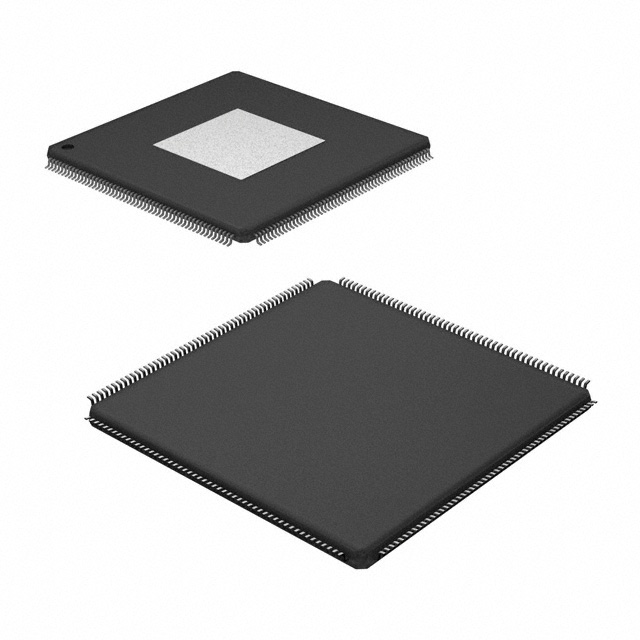
Pinouts................................................................................................72
9.1
Package pinouts and signal descriptions................................. 72
10 Revision History.................................................................................72
SAC57D54H, Rev. 5, 05/2016
4
NXP Semiconductors
�Block diagram
1 Block diagram
RGB
RSDS / RGB
64
64
64
32
32
64
64
64
64
MLB50
32
AHB
AHB
AXI
AXI
AXI
AHB
2D-ACE
HUD Warping
2D-ACE
Tiny UI
ENET-AVB
LDB
OpenVG 1.1
64
64
TCON_1
TCON_0
AHB
16ch eDMA_1
SECURITY
(CSE)
FPU
32KB L1 32KB L1
D-Cache I-Cache
AXI
System
AHB
MBIST
AHB
Code
Temp Sensor
GC355
GPU
NEON
AHB
FPU
16KB L1 16KB L1
D-Cache I-Cache
64KB
TCM
AHB
INT Router
DAP
I/O Ctrl
Reset Ctrl
AHB
16ch eDMA_0
GIC
DMAMUX (64:16)
ARM
Cortex M4
OpenLDI/LVDS
RSDS
ARM
Cortex A5
NVIC
VIU4
System Modules
LVDS
32
Clocking
4-40MHz/32KHz
XOSC
System Bus
Memory Protection
Power
1.2V Regulator
LVD / HVD
64
AHB
Flash memory BIU
64
AHB
64
AHB
AHB
64
AXI
Pixel
Converter
AHB
64
64
AHB
Port Splitter
512kB
System
SRAM (ECC)
512kB
System
SRAM (ECC)
2 - 4MB
Flash memory (ECC)
64
Boot ROM
1.3MB
GRAM
(FlexECC)
EE Emulation
OTP
CA5 GIC
SGM (I2S)
SMC & SSD (6)
Autonomous RTC
Timer/PWM (8ch)
Timer/PWM (8ch)
Timer/PWM (8ch)
Timer/PWM (8ch)
12-bit ADC (24)
CMP (2)
LCD
SWT (3)
PIT (8CH)
STM (4CH)
CRC
SEMA42
UART/LIN (3)
I2C (2)
DSPI (5)
FlexCAN (3)
4k & 2k ETBs
64
AHB
64
AXI
64 AHB 64
DRAM Controller
16/32-bit
SDR
AIPS
Debug
TPIU
AHB
DDR2
Low Power Ctrl
SJTAG
64
QuadSPI
Clock Monitor
AHB
QuadSPI
64
IOP
ARM
CortexM0+
CM4 NVIC
AHB
PLLs
RLE
Decoder
16MHz/128KHz
IRC
Interrupt
Router
Peripheral
Interrupts
32k SRAM
(ECC)
Figure 1. High level block diagram
SAC57D54H, Rev. 5, 05/2016
NXP Semiconductors
5
�Family comparison
320MHz Domain
ARM
Cortex A5
64
64
2D-ACE & HUD
NEON
FPU
64
GC355
OpenVG GPU
AXI
AXI
DAP
32KB L1 32KB L1
D-Cache I-Cache
AXI
AXI
AXI
AXI
64
AXI
64
2D-ACE
ENET-AVB
16CH eDMA
VIU4
System
AHB
Code
AHB
16KB L1 16KB L1
D-Cache I-Cache
MLB50
64KB
TCM
64:16 mux
FPU
SECURITY
(CSE)
ARM
Cortex M4
16CH eDMA
160MHz Domain
64
64
64
64
AHB
AHB
AHB
AHB
M1
64
64
64
64
M0
AHB
RDC - 8 domain, 1MDAC per master, 2x MDAC per CPU.,
32
M3
M2
AHB 64
AHB 64
M4
M5
M7
M13
M8 M9
M14
M10
M11
QoS301
AMBA AXBS
S0
S7
S3
S4
S6 S5
S8 S9 S10 S11
S12
Port Splitter
AIPS 0
AIPS 1
PDAC
PDAC
AHB 64
AHB
64
AHB
64
512kB
System
SRAM (ECC)
AHB
64
AHB
64
AHB
64
S14
S15
Flash Memory
BIU
512kB
System
SRAM (ECC)
4MB
Flash memory (ECC)
S16
SDAC2 [0..3] (AXI)
AHB 64
AHB 64
AHB
64
RLE
Decoder
Boot ROM
S13
SDCAC1 [0..15] (AHB)
SDAC0 [0..15] (AHB)
QuadSPI
S2
QuadSPI
S1
M12
M16
M15
S17
SDAC5 [0..3] (AXI)
AXI 64
Pixel
Converter
1.3MB
GRAM
(FlexECC)
SDAC4 [0..7] (AXI)
Priority Manager
DRAM Controller
16/32-bit
SDR & DDR2
EE Emulation
Secure Flash
memory
OTP
ARM
Cortex M0+
SDAC3 [0..7] (AHB)
AXBS
32kB
SRAM (ECC)
I/O Processor
Figure 2. Detailed block diagram
2 Family comparison
The table below provides a summary of the different members of the SAC57D5xx Low/
Mid-Line Instrument Cluster family and their features. Note that not all features are
available simultaneously on all packages.
Table 1. Feature sets
Product Features
Cores
SAC57D54H
SAC57D53M
SAC57D52L
Cortex-A5 (320 MHz,
32 KB/32 KB L1
Caches, FPU, MMU,
NEON)
Yes
Yes
Yes
Cortex-M4 (160 MHz,
16 KB/16 KB L1
Caches, FPU)
Yes
Yes
Yes
Table continues on the next page...
SAC57D54H, Rev. 5, 05/2016
6
NXP Semiconductors
�Family comparison
Table 1. Feature sets (continued)
Product Features
Internal Memory
SAC57D54H
SAC57D53M
SAC57D52L
Cortex - M0+ I/O
Processor (IOP) (80
MHz)
Yes
Yes
Yes
ECC Flash Memory
4 MB
3 MB
2 MB
1.3 MB
1.3 MB
1.3 MB
System SRAM (ECC)
2 x 512 KB
2 x 512 KB
2 x 512 KB
IOP local SRAM (ECC)
32 KB
32 KB
32 KB
Graphics
External Memory
Interfaces
System and General
Purpose
Graphics/Video/Display/
Audio
System Connectivity
Analog Connectivity
Timer/PWM
Package Options
SRAM1
Dual DDR QuadSPI
2 x Dual DDR QuadSPI 2 x Dual DDR QuadSPI 2 x Dual DDR QuadSPI
16 bit SDR DRAM
(160MHz)
Yes
Yes
Yes
32-Bit DDR2 DRAM
(320MHz)2
Yes
Yes
-
Memory / Peripheral
Protection (xDRC Extended Resource
Domain Controller)
Yes
Yes
Yes
Security (CSE)
Yes
Yes
Yes
eDMA
16ch x 2
16ch x 2
16ch x 2
2D-ACE
x2
x2
x2
HUD Warping Engine
Yes
Yes
Yes
TCON_0/RSDS
Yes
Yes
Yes
TCON_1
Yes
Yes
Yes
OpenLDI/LVDS
Yes
Yes
-
GPU
GC355 : OpenVG 1.1 /
TinyUI
GC355 : OpenVG 1.1 /
TinyUI
GC355 : OpenVG 1.1 /
TinyUI
Video Input Unit
Yes
Yes
Yes
Sound Generator
Yes
Yes
Yes
Segment LCD
Yes
Yes
Yes
FlexCAN
x3
x3
x3
I2C
x2
x2
x2
LINFlexD
x3
x3
x3
SPI
x5
x5
x5
MLB50
Yes
Yes
Yes
10/100 Ethernet + AVB
Yes
Yes
Yes
SMC/SSD
x6
x6
x6
12 Bit ADC
Yes
Yes
Yes
Analog Comparator
2 x 8ch
2 x 8ch
2 x 8ch
PIT
8ch
8ch
8ch
SWT
3
3
3
ARTC
Yes
Yes
Yes
FlexTimer
4 x 8ch
4 x 8ch
4 x 8ch
LQFP
208 LQFP
208 LQFP
208 LQFP
Table continues on the next page...
SAC57D54H, Rev. 5, 05/2016
NXP Semiconductors
7
�Ordering parts
Table 1. Feature sets (continued)
Product Features
BGA
SAC57D54H
SAC57D53M
SAC57D52L
516 MAPBGA
516 MAPBGA
-
1. GRAM can be reconfigured as ECC RAM
2. DDR2 interface only available in BGA package option
3 Ordering parts
3.1 Determining valid orderable parts
Valid orderable part numbers are provided on the web.
1. To determine the orderable part numbers for this device, go to www.nxp.com and
perform a part number search for the following device number: SAC57D5xx.
3.2 Ordering information
SAC57D54H, Rev. 5, 05/2016
8
NXP Semiconductors
�General
4 General
4.1 Absolute maximum ratings
NOTE
Functional operating conditions appear in the DC electrical
characteristics. Absolute maximum ratings are stress ratings
only, and functional operation at the maximum values is not
guaranteed.
Stress beyond the listed maximum values may affect device
reliability or cause permanent damage to the device.
Table 2. Absolute maximum ratings
Symbol 1
VDDE_A, VDDE_B,
VDDE_SDR
VDD_LP_DEC
VDDA
VDDEH_ADC
VSSA
Parameter
Conditions
Min
Max
Unit
Input/output supply voltage2
—
–0.3
3.6
V
Decoupling pin for low power regulators3
—
–0.32
1.32
V
ADC supply voltage
—
–0.3
6.0
V
ADC I/O supply voltage
—
–0.3
6.0
V
ADC supply ground
—
–0.3
0.3
V
VDDA_REF
4
ADC supply voltage
—
–0.3
6.0
V
VDDM_SMD
SMD supply voltage
—
–0.3
6.0
V
VSSM_SMD
SMD supply ground
—
–0.3
0.3
V
VDDE_DDR
DDR2 DRAM supply voltage
—
–0.3
2.3
V
DDR_VREF
DDR I/O Reference Voltage
—
–0.3
1.15
V
Core logic supply voltage
—
–0.3
1.32
V
Relative to
VDDE_A,
VDDE_B,
VDDE_SDR
–0.3
VDDE_ADC + 0.3
V
–0.3
VDDE_A + 0.3
V
Relative to
VDDE_A,
VDDE_B,
VDDE_SDR
–0.3
VDDE_x + 0.3
V
Always
–5
5
mA
5
VDD12
VINA
Voltage on ADC analog pin with respect to
VSSA
Voltage on Analog comparator pin (CMP)
with respect to VSS
VIN
Voltage on any digital pin with respect to
ground (VSS)
IINJPAD
Injected input current on any pin during
overload condition
IINJSUM
Absolute sum of all injected input currents
during overload condition
—
–50
50
mA
Tramp
Supply ramp rate
—
0.5 V / min
100 V/ms
—
Ta 6
Ambient temperature
—
–40
105
°C
TSTG
Storage temperature
—
–55
165
°C
SAC57D54H, Rev. 5, 05/2016
NXP Semiconductors
9
�General
1. All parameters are with reference to Vss unless otherwise specified.
2. A crossover current of up to 2 mA may be experienced if VDD12 is ramped up before VDDE_A supply. This current is only an
electrical crossover but has no functional implications, and should be removed when VDDE_A ramps up to its functional
operating range.
3. Not available for input voltage, only for decoupling internal regulators.
4. VDDA_REF is only available on the 516 BGA package.
5. DDR_VREF is expected to be equal to 0.5 × VDDE_DDR and to track VDDE_DDR DC variations as measured at the device
pins. Ensure VDD_LV supply ramps up before VDDE_DDR. In Standby mode, it should be ensured that VDDE_DDR supply
should be cut off.
6. Tj=125°C. Assumes Ta=105°C. Assumes maximum θJA of 2s2p board. See Thermal attributes section for details.
4.2 Recommended operating conditions
The following table describes the operating conditions for the device, and for which all
specifications in the data sheet are valid, except where explicitly noted. The device
operating conditions must not be exceeded in order to guarantee proper operation and
reliability. The ranges in this table are design targets and actual data may vary in the
given range.
For normal device operations, VDDE_A, VDDA, VDDA_REF, VDDEH_ADC and VDD12
supplies must be within operating range corresponding to the range mentioned in
following tables. This is required even if some of the features are not used. If using the
ADC to convert SSD channels then VDDA should always be >= VDDM_SMC.
VDD12 should be supplied externally. VDDA_REF, the supply port to 516 BGA is shorted to
VDDA inside lower pin packages. Stepper Stall Detect module (SSD) should only be
operated in the 4.5 V to 5.5 V range and so cannot be used if VDDM_SMD is in 3.3 V
range.
Design may experience up to 30 mA additional crossover current (on VDDE_A) if the
high voltage flash supply is powered before the low voltage core supply. This additional
current will be removed once VDD12 supply rises to its operating range. There is no
reliability concern to the device due to this additional current.
Table 3. Recommended operating conditions
Symbol 1
Parameter
Conditions
Min2
Max
Unit
VDDE_A
Input/output supply voltage
—
3.15
3.6
V
VSSA
ADC supply ground, relative to
VSS
—
-0.1
0.1
V
VDDA
ADC supply voltage
3.15
5.5
V
VDDEH_ADC
ADC I/O supply voltage
3.15
5.5
V
VDDA_REF
ADC reference voltage
VDDA,VDDA_REF and VDDEH_ADC
should be within +/-25 mV of
each other
3.15
5.5
V
VDDM_SMD
SMD supply voltage
—
3.15
5.5
V
VDDE_B3
VDDE_SDR3
Table continues on the next page...
SAC57D54H, Rev. 5, 05/2016
10
NXP Semiconductors
�General
Table 3. Recommended operating conditions (continued)
Symbol 1
Parameter
Conditions
Min2
Max
Unit
VDDE_DDR
DDR2 supply voltage
—
1.7
1.9
V
DDR_VREF
DDR I/O Reference Voltage
—
VDDE_DDR
(min)/2
VDDE_DDR
(max)/2
V
VDD124
Core logic supply voltage
—
1.20
1.32
V
VSSEH_ADC
ADC supply ground, relative to
VSS
—
-0.3
0.3
V
IINJPAD
Injected input current on any
pin during overload condition
—
-3.0
3.0
mA
Ta5
Ambient temperature under
bias
–40
105
°C
1. All parameters are with reference to Vss, unless otherwise specified.
2. Device will be functional (and electrical specifications as per various datasheet parameters will be guaranteed) until one of
the LVD/HVD resets the device. When voltage drops outside range for an LVD/HVD, device is reset.
3. VDDE_A, VDDE_B and VDDE_SDR are all independent supplies and can each be set to 3.3 V. However, care must be taken
over LCD inputs that operate across the IO segments.
4. Only applicable when supplying from external source. VDD12 supply pins should never be grounded (through a small
impedance). If not driven, these should only be left floating.
5. Tj=125°C. Assumes Ta=105°C. Assumes maximum θJA of 2s2p board. See Thermal attributes section for details.
4.3 Voltage regulator electrical specifications
The voltage regulator is composed of the following blocks:
• Connect an external 1.25 V nominal directly
• Low voltage detector - low threshold (LVD_HV_A) for VDDE_A supply
• Low voltage detector (LVD_FLASH) for 3.3 V flash supply
• Various low voltage detectors (LVD_LV_x) for digital core supply (VDD12)
• High voltage detector (HVD_LV) for digital core supply (VDD12)
• Power on Reset (POR_LV) for 1.25 V digital core supply (VDD12)
• Power on Reset (POR_HV) for VDDE_A
SAC57D54H, Rev. 5, 05/2016
NXP Semiconductors
11
�General
LPPREG
VDD_LP_DEC
ULPPREG
CLP/ULPREG
Vss
V DD12
Vss
DEVICE
Figure 3. Voltage regulator capacitance connection
Table 4. Voltage regulator electrical specifications
Symbol
Clp/ulp_reg
Parameter
Conditions
External decoupling / stability
Min, max values shall be
capacitor for internal low power granted with respect to
regulators
tolerance, voltage, temperature,
and aging variations
Combined ESR of external
capacitor
—
Min
Typ1
Max
Unit
0.8
1
1.4
µF
0.001
—
0.1
Ohm
1. Typical values will vary over temperature, voltage, tolerance, drift, but total variation must not exceed minimum and
maximum values.
4.3.1 Recommended decoupling capacitor values
Following are the recommendations for supply decoupling on various power domains:
• For VDDE_A, VDDE_B, VDDE_SDR, VDDM_SMD, VDDE_DDR, VDDA,
VDDEH_ADC,VDDA_REF, DDR_VREF supplies:
• 0.1 μF close to each VDD/VSS pin pair.
• 1 μF on each side of the chip for each supply domain.
• 10 μF near for each power supply source (except for VDDM_SMD pins where a
higher capacitance value may be needed depending upon motor characteristics).
SAC57D54H, Rev. 5, 05/2016
12
NXP Semiconductors
�General
• For VDD12, 0.1 μF close to each VDD/VSS pin pair is required.
4.4 Voltage monitor electrical specifications
Table 5. Voltage monitor electrical specifications
Symbol
Parameter
State Conditions
Configuration
Power
Up 1
VPOR_LV
LV supply
power on reset
detector
Fall
Rise
Typ
Max
0.9300
0.9790
1.0280
V
Trimmed
-
-
-
V
Untrimmed
0.9800
1.0290
1.0780
V
-
-
-
V
1.3750
V
Yes
No
Reset Type
Destructive
Trimmed
VHVD_LV_cold
VLVD_LV_PD2_hot
VLVD_LV_PD1_hot
VLVD_LV_PD0_hot
VPOR_HV
VLVD_IO_A_LO
LV supply high Fall
voltage
monitoring,
detecting at the Rise
device pin
Untrimmed
LV supply low Fall
voltage
monitoring,
detecting in the Rise
PD2 core (hot)
area
Untrimmed
LV supply low Fall
voltage
monitoring,
detecting in the Rise
PD1 core (hot)
area
Untrimmed
LV supply low Fall
voltage
monitoring,
detecting in the Rise
PD0 core (hot)
area
Untrimmed
HV supply
power on reset
detector
Untrimmed
Fall
Rise
HV IO_A supply Fall
low voltage
monitoring - low
Rise
range
VLVD_LV_PD2_COL LV supply low Fall
voltage
D
monitoring,
detecting at the Rise
device pin
Unit
Min
Untrimmed
Mask
Opt
Threshold
No
Yes
Functional
Disabled at Start
Trimmed
1.3250
Untrimmed
Disabled at Start
Trimmed
1.3450
1.3650
1.3950
V
1.0800
1.1200
1.1600
V
Trimmed
1.1250
1.1425
1.1600
V
Untrimmed
1.1000
1.1400
1.1800
V
Trimmed
1.1450
1.1625
1.1800
V
Yes
1.0800
1.1200
1.1600
V
1.1140
1.1370
1.1600
V
Untrimmed
1.1000
1.1400
1.1800
V
Trimmed
1.1340
1.1570
1.1800
V
1.0800
1.1200
1.1600
V
Trimmed
1.1140
1.1370
1.1600
V
Untrimmed
1.1000
1.1400
1.1800
V
Trimmed
1.1340
1.1570
1.1800
V
2.7000
2.8500
3.0000
V
Trimmed
-
-
-
V
Untrimmed
2.7500
2.9000
3.0500
V
Trimmed
-
-
-
V
2.7500
2.9230
3.0950
V
Trimmed
2.9780
3.0390
3.1000
V
Untrimmed
2.7800
2.9530
3.1250
V
Trimmed
3.0080
3.0690
3.1300
V
1.1750
V
1.1950
V
Untrimmed
Yes
Yes
Yes
No
No
Destructive
Trimmed
Untrimmed
Yes
No
No
No
No
Yes
Destructive
1.3450
Destructive
Destructive
Destructive
Functional
Disabled at Start
Trimmed
1.1400
1.1550
Untrimmed
Disabled at Start
Trimmed
1.1600
1.1750
SAC57D54H, Rev. 5, 05/2016
NXP Semiconductors
13
�General
1. All monitors that are active at power up will gate the power up recovery and prevent exit from POWERUP phase until the
minimum level is crossed. These monitors can in some cases be masked during normal device operation, but when active
will always generate a destructive reset.
4.5 Power consumption
The following table shows the power consumption for the device in the various modes of
operation.
Table 6. Power consumption
Mode
Configuration
Typ
Max
Unit
Run Mode
CA5 320 MHz, CM4
160 MHz, DDR2 320
MHz, Dual Display (516
BGA)
800
1500
mA
Run Mode
CA5 320 MHz, CM4
160 MHz, SDR 160
MHz, Single Display
(208 QFP)
600
1200
mA
IOP Run Mode
CM0+ 16 MHz, PD1/0
domains powered,
remainder of device
power gated off.
31
35
mA
IOP Stop Mode
CM0+ halted, PD1/0
domains powered, all
module enabled and
LCD running in IOP
domain, remainder of
device power gated off.
0.252
20
mA
Stop Mode
Cores halted, Device
fully powered.
240
700 3
mA
Standby Mode4, 5
ARTC/32 KHz + 32 KB
SRAM powered
μA
ARTC/32 KHz + 8 KB
SRAM powered
50 (25 °C)
70 (25 °C)
500 (55 °C)
900 (55 °C)
1500 (85 °C)
2500 (85 °C)
2000 (105 °C)
4000 (105 °C)
45 (25 °C)
65 (25 °C)
500 (55 °C)
900 (55 °C)
1500 (85 °C)
2500 (85 °C)
2000 (105 °C)
4000 (105 °C)
μA
IOP_Run typical is measured at 25oC.
IOP_Stop typical is measured at 25oC.
There could be 10% variation based on the characterization.
Weak pull functionality provided in I/O pads must be used to configure I/Os in a known state (that does not cause
contention with external connection on the pin) to avoid floating input to cause crow-bar currents and hence increased
leakage during low power modes.
5. During STANDBY/IOP modes, it is recommended to keep VDDE_A, VDDEH_ADC, VDDAand VDDA_REF powered to their
respective functional levels to obtain best power performance of the device. All other supplies are recommended be kept
unpowered in these low power modes.
1.
2.
3.
4.
SAC57D54H, Rev. 5, 05/2016
14
NXP Semiconductors
�General
The following diagrams show the supply configuration of the device.
Figure 4. Supply configuration
4.6 Electrostatic discharge (ESD) specifications
Electrostatic discharges (a positive then a negative pulse separated by 1 second) are
applied to the pins of each sample according to each pin combination. The sample size
depends on the number of supply pins in the device (3 parts × (n + 1) supply pin). This
test conforms to the AEC-Q100-002/-003/-011 standard.
NOTE
A device will be defined as a failure if after exposure to ESD
pulses the device no longer meets the device specification
requirements. Complete DC parametric and functional testing
shall be performed per applicable device specification at room
temperature followed by hot temperature, unless specified
otherwise in the device specification.
Table 7. ESD ratings
Symbol
VESD(HBM)
Conditions1
Parameter
Electrostatic discharge
TA = 25 °C
Class
Max value2
Unit
H1C
2000
V
(Human Body Model)
Table continues on the next page...
SAC57D54H, Rev. 5, 05/2016
NXP Semiconductors
15
�I/O parameters
Table 7. ESD ratings (continued)
Symbol
Conditions1
Parameter
Class
Max value2
Unit
C3A
500
V
conforming to AECQ100-002
VESD(CDM)
Electrostatic discharge
TA = 25 °C
(Charged Device Model)
conforming to AECQ100-011
750 (corners)
1. All ESD testing is in conformity with CDF-AEC-Q100 Stress Test Qualification for Automotive Grade Integrated Circuits.
2. Data based on characterization results, not tested in production.
4.7 Electromagnetic Compatibility (EMC) specifications
EMC measurements to IC-level IEC standards are available from NXP on request.
5 I/O parameters
5.1 AC specifications @ 3.3 V range
Table 8. Functional Pad AC Specifications @ 3.3 V range
Symbol
Rise/Fall Edge (ns)
Min
pad_sr_hv
(output)
Drive Load (pF)
Max
1.75/1.5
MSB, LSB
25
0.8/0.8
3.25/3
50
3.5/2.5
12/12
200
0.6/0.8
3.75/3.5
25
1/1
7/6.5
50
7.7/5
25/21
200
4/3.5
25/25
50
6.3/6.2
30/30
200
6.8/6
40/40
50
11/11
Drive/Slew Rate Select
11 (Recommended setting)
10
01
001
51/51
200
0.5/0.5
0.5
NA
1.5/1.5
30
11
2.4/2.4
50
0.6/0.6
1.5/1.5
20
10
0.6/0.6
1.85/1.85
10
01
12/11
36/45
50
00
pad_i_hv/pad_sr_hv
(input)2
pad_fc_hv
(output)
0.6/0.6
SAC57D54H, Rev. 5, 05/2016
16
NXP Semiconductors
�I/O parameters
1. Slew rate control modes
2. Input slope = 2 ns
5.2 DC electrical specifications @ 3.3 V range
Table 9. DC electrical specifications @ 3.3 V range
Symbol
Vdde
Parameter
I/O Supply Voltage
Value
Unit
Min
Max
3.15
3.63
V
Vih
CMOS Input Buffer High Voltage (with
hysteresis disabled)
0.55 x Vdde
Vdde + 0.3
V
Vil
CMOS Input Buffer Low Voltage (with
hysteresis disabled)
Vss − 0.3
0.40 x Vdde
V
Vih_hys
CMOS Input Buffer High Voltage (with
hysteresis enabled)
0.65 x Vdde
Vdde + 0.3
V
Vil_hys
CMOS Input Buffer Low Voltage (with
hysteresis enabled)
Vss − 0.3
0.35 x Vdde
V
CMOS Input Buffer Hysteresis
0.1 x Vdde
Vhys
V
Pull_Ioh_vil_hys
Weak Pullup Current measured when
pad = 0.35 x Vdde
25
80
µA
Pull_Ioh_vih_hys
Weak Pulldown Current measured when
pad = 0.65 x Vdde
25
80
µA
Iinact_d
Digital Pad Input Leakage Current (weak
pull inactive)
−2.5
2.5
µA
0.8 x Vdde
—
V
—
0.2 x Vdde
V
Voh
Output High Voltage1
Vol
Voltage2
Output Low
Vih_ttl
TTL High Level Input Voltage
Vil_ttl
TTL Low Level Input Voltage
Vhyst_ttl
TTL Input Hysteresis Voltage
Vih_auto
Automotive High Level Input Voltage
Vil_auto3
Vhyst_auto
1.8
V
0.6
0.25
V
V
0.75 x Vdde
Vdde + 0.3
V
Automotive Low Level Input Voltage
−0.3
0.35 ✕ Vdde
V
Automotive Input Hysteresis Voltage
0.11 x Vdde
V
1. Measured when pad is sourcing 2 mA.
2. Measured when pad is sinking 2 mA.
3. Auto levels are applicable to the ‘input only' channels (CH0-7) of the ADC pins
SAC57D54H, Rev. 5, 05/2016
NXP Semiconductors
17
�I/O parameters
5.3 AC specifications @ 5 V range
Table 10. Functional pad AC specifications @ 5 V range
Symbol
Rise/Fall Edge (ns)
Min
pad_sr_hv
Drive Load (pF)
Max
MSB, LSB
1.2/1.2
(output)
pad_fc_hv
(output)
Drive/Slew Rate Select
25
11 (Recommended setting)
2.5/2
50
8/8
200
3/2
25
5/4
50
18/16
200
13/13
50
24/24
200
24/24
50
10
01
001
50/50
200
1.8/1.7
50
6.6/6.1
200
2.7/2.5
50
10.3/9.3
200
5.6/4.8
50
21/19
200
41/41
50
151/151
200
11
10
01
00
1. Slew rate control modes
5.4 DC electrical specifications @ 5 V range
Table 11. DC electrical specifications @ 5 V range
Symbol
Vdde
Parameter
I/O Supply Voltage
Value
Unit
Min
Max
4.5
5.5
V
Vih
CMOS Input Buffer High Voltage (with hysteresis
disabled)
0.55 × Vdde
Vdde + 0.3
V
Vil
CMOS Input Buffer Low Voltage (with hysteresis
disabled)
Vss − 0.3
0.40 × Vdde
V
Vih_hys
CMOS Input Buffer High Voltage (with hysteresis
enabled)
0.65 × Vdde
Vdde + 0.3
V
Vil_hys
CMOS Input Buffer Low Voltage (with hysteresis
enabled)
Vss − 0.3
0.35 × Vdde
V
Table continues on the next page...
SAC57D54H, Rev. 5, 05/2016
18
NXP Semiconductors
�I/O parameters
Table 11. DC electrical specifications @ 5 V range (continued)
Symbol
Parameter
Value
Min
Vhys
CMOS Input Buffer Hysteresis
Unit
Max
0.1 × Vdde
V
Pull_Ioh_vil_h ys
Weak Pullup Current measured when pad = 0.35 x Vdde
(Vil_hys)
40
120
µA
Pull_Ioh_vih_hys
Weak Pulldown Current measured when pad = 0.65 x
Vdde (Vih_hys)
40
120
µA
Iinact_d
Digital Pad Input Leakage Current (weak pull inactive)
−2.5
2.5
µA
Voltage1
Voh
Output High
0.8 x Vdde
—
V
Vol
Output Low Voltage2
—
0.2 x Vdde
V
Vih_ttl
TTL High Level Input Voltage
2.0
Vil_ttl
TTL Low Level Input Voltage
Vhyst_ttl
TTL Input Hysteresis Voltage
0.3
Vih_auto
Automotive High Level Input Voltage
3.8
Vdde + 0.3
V
Automotive Low Level Input Voltage
−0.3
2.2
V
Vhyst_auto
Automotive Input Hysteresis Voltage
0.5
Vih_auto3
Automotive High Level Input Voltage
0.7 × Vdde
Vdde + 0.3
V
Vil_auto3
Automotive Low Level Input Voltage
−0.3
0.47 × Vdde
V
Automotive Input Hysteresis Voltage
0.11 × Vdde
3
Vil_auto
3
V
0.8
V
V
V
Automotive Levels with Expanded VDDE Range: 4 V - 5.5 V
3
Vhyst_auto
V
1. Measured when pad is sourcing 2 mA.
2. Measured when pad is sinking 2 mA.
3. Auto levels are applicable to the ‘input only' channels (CH0-7) of the ADC pins
5.5 DDR2 pads IO specifications
5.5.1 DDR2 pads AC specifications @ 1.8V VDDE_DDR
Table 12. DDR2 pads AC electrical specifications at 1.8 V VDDE_DDR
Name
pad_dq_18
Rise/Fall Edge (V/ns)
Drive Load (pF)
Drive Strength
Select (Refer
SIUL_MSCR[SRE]
description in the
device reference
manual)
Min
Max
Half/Full
1
—
5
Half
1
—
20
Half
1
—
5
Full
Table continues on the next page...
SAC57D54H, Rev. 5, 05/2016
NXP Semiconductors
19
�I/O parameters
Table 12. DDR2 pads AC electrical specifications at 1.8 V VDDE_DDR (continued)
Name
Rise/Fall Edge (V/ns)
pad_acc_18
pad_clk_18
Drive Load (pF)
Drive Strength
Select (Refer
SIUL_MSCR[SRE]
description in the
device reference
manual)
Min
Max
Half/Full
1
—
20
Full
1
—
5
Half
1
—
20
Half
1
—
5
Full
1
—
20
Full
1
—
5
Half
1
—
20
Half
1
—
5
Full
1
—
20
Full
5.5.2 SSTL_18 Class II 1.8 V DDR2 DC specifications
Table 13. SSTL_18 Class II 1.8 V DDR2 DC specifications
Symbol
Parameter
Conditio
n
Min
Typ
Max
Uni
t
Notes
VDDE_DDR
DDR 1.8 V I/O
Supply voltage
—
1.7
1.8
1.9
V
VDD12
Core Supply
Voltage
—
1.20
1.26
1.32
V
A5.15
DDR_REF
I/O Reference
Voltage
—
0.51 x
VDDE_DDR
V
A5.16
Vih(dc)
DC Input Logic
High
—
Vil(dc)
DC Input Logic
Low
—
Vih(ac)
AC Input Logic
High
—
Vil(ac)
AC Input Logic
Low
Iin
0.49 x VDDE_DDR 0.50 x VDDE_DDR
DDR_VREF +
0.125
—
JESD8-15
A
SpecI
D
A5.14
V
JESD8-15
A
A5.18
—
DDR_VREF −
0.125
V
JESD8-15
A
A5.19
DDR_VREF +
0.25
—
—
V
JESD8-15
A
A5.20
—
—
—
DDR_VREF −
0.25
V
JESD8-15
A
A5.21
Pad input
Leakage Current
—
-50
—
50
μA —
A5.22
Voh
Output High
Voltage Level
—
VDDE_DDR − 0.28
—
—
V
—
A5.23
Vol
Output Low
Voltage Level
—
—
—
0.28
V
—
A5.24
Table continues on the next page...
SAC57D54H, Rev. 5, 05/2016
20
NXP Semiconductors
�SMC pads IO specifications
Table 13. SSTL_18 Class II 1.8 V DDR2 DC specifications (continued)
Symbol
Parameter
Conditio
n
Min
Typ
Max
Uni
t
Notes
SpecI
D
Ioh(dc)
Output min
Vout = Voh
source dc current
−12.86
—
—
mA JESD8-15
A VDDE_DDR
= 1.7V Voh
= 1.42V
A5.25
Iol(dc)
Output min sink
dc current
12.86
—
—
mA JESD8-15
A VDDE_DDR
= 1.7 V Vol
= 0.28 V
A5.26
Vout= Vol
Table 14. Current-draw Characteristics for DDR_VREF
Symbol
DDR_VREF
Parameter
Current-draw characteristics for DDR_VREF
Min
Max
Unit
-
5
mA
5.6 SMC pads IO specifications
5.6.1 SMC 5V pads IO specifications
NOTE
In Table 15, Table 16, "VDDE" is the VDDM_SMD supply
5.6.1.1
SMC 5V pads IO DC specifications
Table 15. SMC 5V IO DC specifications(4.5V