Freescale Semiconductor
Data Sheet: Technical Data
Document Number: MPC5200BDS
Rev. 4, 02/2010
MPC5200B Data Sheet
Key features are shown below.
• MPC603e series e300 core
– Superscalar architecture
– 760 MIPS at 400 MHz (–40 oC to +85 oC)
– 16 KB Instruction cache, 16 KB Data cache
– Double precision FPU
– Instruction and Data MMU
– Standard and Critical interrupt capability
• SDRAM / DDR Memory Interface
– Up to 133 MHz operation
– SDRAM and DDR SDRAM support
– 256 MB addressing range per CS, two CS available
– 32-bit data bus
– Built-in initialization and refresh
• Flexible multi-function External Bus Interface
– Supports interfacing to ROM/Flash/SRAM memories or
other memory mapped devices
– 8 programmable Chip Selects
– Non-multiplexed data access using 8-/16-/32-bit databus
with up to 26-bit address
– Short or Long Burst capable
– Multiplexed data access using 8-/16-/32-bit databus
with up to 25-bit address
• Peripheral Component Interconnect (PCI) Controller
– Version 2.2 PCI compatibility
– PCI initiator and target operation
– 32-bit PCI Address/Data bus
– 33 and 66 MHz operation
– PCI arbitration function
• ATA Controller
– Version 4 ATA compatible external interface—IDE Disk
Drive connectivity
• BestComm DMA subsystem
– Intelligent virtual DMA Controller
– Dedicated DMA channels to control peripheral
reception and transmission
– Local memory (SRAM 16 KB)
• 6 Programmable Serial Controllers (PSC)
– UART or RS232 interface
– CODEC interface for Soft Modem, Master/Slave
CODEC Mode, I2S and AC97
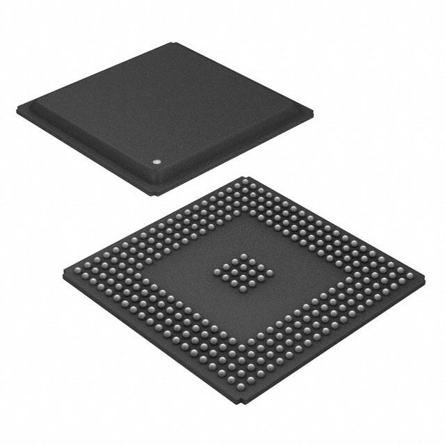
TEPBGA–272
27 mm x 27 mm
•
•
•
•
•
•
•
•
•
•
•
•
– Full duplex SPI mode
– IrDA mode from 2400 bps to 4 Mbps
Fast Ethernet Controller (FEC)
– Supports 100Mbps IEEE 802.3 MII, 10 Mbps IEEE
802.3 MII, 10 Mbps 7-wire interface
Universal Serial Bus Controller (USB)
– USB Revision 1.1 Host
– Open Host Controller Interface (OHCI)
– Integrated USB Hub, with two ports.
Two Inter-Integrated Circuit Interfaces (I2C)
Serial Peripheral Interface (SPI)
Dual CAN 2.0 A/B Controller (MSCAN)
– Implementation of version 2.0A/B CAN protocol
– Standard and extended data frames
J1850 Byte Data Link Controller (BDLC)
J1850 Class B data communication network interface
compatible and ISO compatible for low speed ( LB = 1
Data bus width is 8 bit. => DS = 8
=> 41 × 2 × (32/8) = 32 => ACK is asserted for 32 PCI cycles to transfer one cache line.
Wait State is set to 10. => WS = 10
1 + 10 + 32 = 43 => CS is asserted for 43 PCI cycles.
3. ACK is output and indicates the burst.
4. Deadcycles are only used, if no arbitration to an other module (ATA or PCI) of the shared local bus happens. If arbitration
happens the bus can be driven within 4 IPB clocks by an other modules.
PCI CLK
CS[x]
t1
t2
t3
ADDR
t5
t4
OE
t6
t7
R/W
t8
t10
DATA (rd)
t9
t11
t12
ACK
t14
t15
t13
TS
Figure 12. Timing Diagram—Burst Mode
MPC5200B Data Sheet, Rev. 4
26
Freescale Semiconductor
�1.3.8.3
MUXed Mode
Table 26. MUXed Mode Timing
Sym
Description
Min
Max
Units
Notes
SpecID
t CSA
PCI CLK to CS assertion
4.6
10.6
ns
—
A7.39
t CSN
PCI CLK to CS negation
2.9
7.0
ns
—
A7.40
tALEA
PCI CLK to ALE assertion
—
3.6
ns
—
A7.41
t1
ALE assertion before Address, Bank,
TSIZ assertion
—
5.7
ns
—
A7.42
t2
CS assertion before Address, Bank,
TSIZ negation
—
–1.2
ns
—
A7.43
t3
CS assertion before Data wr valid
—
–1.2
ns
—
A7.44
t4
Data wr hold after CS negation
tIPBIck
—
ns
—
A7.45
t5
Data rd setup before CS negation
8.5
—
ns
—
A7.46
t6
Data rd hold after CS negation
0
(DC + 1) × tPCIck
ns
(1),(3)
A7.47
t7
ALE pulse width
—
tPCIck
ns
—
A7.48
tTSA
CS assertion after TS assertion
—
6.9
ns
—
A7.49
t8
TS pulse width
—
tPCIck
ns
—
A7.50
t9
CS pulse width
ns
—
A7.51
tOEA
OE assertion before CS assertion
—
4.7
ns
—
A7.52
tOEN
OE negation before CS negation
—
5.9
ns
—
A7.53
t10
RW assertion before ALE assertion
tIPBIck
—
ns
—
A7.54
t11
RW negation after CS negation
—
tPCIck
ns
—
A7.55
t12
ACK assertion after CS assertion
tIPBIck
—
ns
(2)
A7.56
(2)
A7.57
(2 + WS) × tPCIck (2 + WS) × tPCIck
t13
ACK negation after CS negation
—
tPCIck
ns
t14
ALE negation to CS assertion
—
tPCIck
ns
A7.58
t15
ACK change before PCI clock
—
2.0
ns
(2)
t16
ACK change after PCI clock
—
4.4
ns
(2)
A7.59
A7.60
NOTES:
1. ACK can shorten the CS pulse width.
Wait States (WS) can be programmed in the Chip Select X Register, Bit field WaitP and WaitX. It can be specified from
0–65535.
2. ACK is input and can be used to shorten the CS pulse width.
3. Deadcycles are only used, if no arbitration to an other module (ATA or PCI) of the shared local bus happens. If arbitration
happens the bus can be driven within 4 IPB clocks by an other modules.
MPC5200B Data Sheet, Rev. 4
Freescale Semiconductor
27
�PCI CLK
t2
t1
t4
AD[31,27] (wr)
Data
AD[30:28] (wr)
TSIZ[0:2] bits
Data
AD[26:25] (wr)
Bank[0:1] bits
Data
AD[24:0] (wr)
Address[7:31]
Data
t3
t5
AD[31:0] (rd)
t6
Data
t7
t14
ALE
t8
Address latch
TS
t9
CSx
OE
t10
t11
R/W
t16
t12
ACK
t15
Address tenure
t13
Data tenure
Figure 13. Timing Diagram—MUXed Mode
1.3.9
ATA
The MPC5200B ATA Controller is completely software programmable. It can be programmed to operate with ATA protocols
using their respective timing, as described in the ANSI ATA-4 specification. The ATA interface is completely asynchronous in
nature. Signal relationships are based on specific fixed timing in terms of timing units (nanoseconds).
ATA data setup and hold times, with respect to Read/Write strobes, are software programmable inside the ATA Controller. Data
setup and hold times are implemented using counters. The counters count the number of ATA clock cycles needed to meet the
ANSI ATA-4 timing specifications. For details, see the ANSI ATA-4 specification and how to program an ATA Controller and
ATA drive for different ATA protocols and their respective timing. See the MPC5200B User’s Manual (MPC5200BUM).
The MPC5200B ATA Host Controller design makes data available coincidentally with the active edge of the WRITE strobe in
PIO and Multiword DMA modes.
•
•
Write data is latched by the drive at the inactive edge of the WRITE strobe. This gives ample setup time beyond that
required by the ATA-4 specification.
Data is held unchanged until the next active edge of the WRITE strobe. This gives ample hold time beyond that
required by the ATA-4 specification.
MPC5200B Data Sheet, Rev. 4
28
Freescale Semiconductor
�All ATA transfers are programmed in terms of system clock cycles (IP bus clocks) in the ATA Host Controller timing registers.
This puts constraints on the ATA protocols and their respective timing modes in which the ATA Controller can communicate
with the drive.
Faster ATA modes (i.e., UDMA 0, 1, 2) are supported when the system is running at a sufficient frequency to provide adequate
data transfer rates. Adequate data transfer rates are a function of the following:
• The MPC5200B operating frequency (IP bus clock frequency)
• Internal MPC5200B bus latencies
• Other system load dependent variables
The ATA clock is the same frequency as the IP bus clock in MPC5200B. See the MPC5200B User’s Manual (MPC5200B).
NOTE
All output timing numbers are specified for nominal 50 pF loads.
Table 27. PIO Mode Timing Specifications
Sym
PIO Timing Parameter
Min/Max
(ns)
Mode 0
(ns)
Mode 1
(ns)
Mode 2
(ns)
Mode 3
(ns)
Mode 4
(ns)
SpecID
t0
Cycle Time
min
600
383
240
180
120
A8.1
t1
Address valid to DIOR/DIOW setup
min
70
50
30
30
25
A8.2
t2
DIOR/DIOW pulse width 16-bit
8-bit
min
min
165
290
125
290
100
290
80
80
70
70
A8.3
t2i
DIOR/DIOW recovery time
min
—
—
—
70
25
A8.4
t3
DIOW data setup
min
60
45
30
30
20
A8.5
t4
DIOW data hold
min
30
20
15
10
10
A8.6
t5
DIOR data setup
min
50
35
20
20
20
A8.7
t6
DIOR data hold
min
5
5
5
5
5
A8.8
t9
DIOR/DIOW to address
valid hold
min
20
15
10
10
10
A8.9
tA
IORDY setup
max
35
35
35
35
35
A8.10
tB
IORDY pulse width
max
1250
1250
1250
1250
1250
A8.11
MPC5200B Data Sheet, Rev. 4
Freescale Semiconductor
29
�CS[0]/CS[3]/DA[2:0]
t2
DIOR/DIOW
t9
t1
t0
t3
t4
WDATA
t5
t6
RDATA
tA
tB
IORDY
Figure 14. PIO Mode Timing
Table 28. Multiword DMA Timing Specifications
Sym
Multiword DMA Timing Parameters
Min/Max
Mode 0(ns)
Mode 1(ns)
Mode 2(ns)
SpecID
t0
Cycle Time
min
480
150
120
A8.12
tC
DMACK to DMARQ delay
max
—
—
—
A8.13
tD
DIOR/DIOW pulse width (16-bit)
min
215
80
70
A8.14
tE
DIOR data access
max
150
60
50
A8.15
tG
DIOR/DIOW data setup
min
100
30
20
A8.16
tF
DIOR data hold
min
5
5
5
A8.17
tH
DIOW data hold
min
20
15
10
A8.18
tI
DMACK to DIOR/DIOW setup
min
0
0
0
A8.19
tJ
DIOR/DIOW to DMACK hold
min
20
5
5
A8.20
tKr
DIOR negated pulse width
min
50
50
25
A8.21
tKw
DIOW negated pulse width
min
215
50
25
A8.22
tLr
DIOR to DMARQ delay
max
120
40
35
A8.23
tLw
DIOW to DMARQ delay
max
40
40
35
A8.24
MPC5200B Data Sheet, Rev. 4
30
Freescale Semiconductor
�t0
DMARQ
(Drive)
tL
tC
DMACK
(Host)
tD
tI
tJ
tK
DIOR
DIOW
(Host)
tE
RDATA
(Drive)
tF
WDATA
(Host)
tG
tH
Figure 15. Multiword DMA Timing
NOTE
The direction of signal assertion is towards the top of the page, and the direction of negation
is towards the bottom of the page, irrespective of the electrical properties of the signal.
Table 29. Ultra DMA Timing Specification
Sym
MODE 0
(ns)
MODE 1
(ns)
MODE 2
(ns)
Comment
SpecID
Min
Max
Min
Max
Min
Max
t CYC
114
—
75
—
55
—
Cycle time allowing for asymmetry and clock
variations from STROBE edge to STROBE edge
A8.26
t 2CYC
235
—
156
—
117
—
Two-cycle time allowing for clock variations, from
rising edge to next rising edge or from falling edge to
next falling edge of STROBE.
A8.27
t DS
15
—
10
—
7
—
Data setup time at recipient.
A8.28
t DH
5
—
5
—
5
—
Data hold time at recipient.
A8.29
t DVS
70
—
48
—
34
—
Data valid setup time at sender, to STROBE edge.
A8.30
t DVH
6
—
6
—
6
—
Data valid hold time at sender, from STROBE edge.
A8.31
t FS
0
230
0
200
0
170
First STROBE time for drive to first negate DSTROBE
from STOP during a data-in burst.
A8.32
t LI
0
150
0
150
0
150
Limited Interlock time.
A8.33
t MLI
20
—
20
—
20
—
Interlock time with minimum.
A8.34
t UI
0
—
0
—
0
—
Unlimited interlock time.
A8.35
MPC5200B Data Sheet, Rev. 4
Freescale Semiconductor
31
�Table 29. Ultra DMA Timing Specification (continued)
Sym
MODE 0
(ns)
MODE 1
(ns)
MODE 2
(ns)
Comment
SpecID
Min
Max
Min
Max
Min
Max
t AZ
—
10
—
10
—
10
Maximum time allowed for output drivers to release
from being asserted or negated
A8.36
t ZAH
20
—
20
—
20
—
A8.37
t ZAD
0
—
0
—
0
—
Minimum delay time required for output drivers to
assert or negate from released state
t ENV
20
70
20
70
20
70
Envelope time—from DMACK to STOP and
HDMARDY during data out burst initiation.
A8.39
t SR
—
50
—
30
—
20
STROBE to DMARDY time, if DMARDY is negated
before this long after STROBE edge, the recipient
receives no more than one additional data word.
A8.40
t RFS
—
75
—
60
—
50
Ready-to-Final STROBE time—no STROBE edges
are sent this long after negation of DMARDY.
A8.41
t RP
160
—
125
—
100
—
Ready-to-Pause time—the time recipient waits to
initiate pause after negating DMARDY.
A8.42
t IORDYZ
—
20
—
20
—
20
Pull-up time before allowing IORDY to be released.
A8.43
t ZIORDY
0
—
0
—
0
—
Minimum time drive waits before driving IORDY
A8.44
t ACK
20
—
20
—
20
—
Setup and hold times for DMACK, before assertion or
negation.
A8.45
t SS
50
—
50
—
50
—
Time from STROBE edge to negation of DMARQ or
assertion of STOP, when sender terminates a burst.
A8.46
A8.38
NOTES:
1 t UI, t MLI, t LI indicate sender-to-recipient or recipient-to-sender interlocks. That is, one agent (sender or recipient) is waiting for
the other agent to respond with a signal before proceeding.
• t UI is an unlimited interlock that has no maximum time value.
• t MLI is a limited time-out that has a defined minimum.
• t LI is a limited time-out that has a defined maximum.
2 All timing parameters are measured at the connector of the drive to which the parameter applies. For example, the sender shall
stop generating STROBE edges t RFS after negation of DMARDY. STROBE and DMARDY timing measurements are taken at
the connector of the sender. Even though the sender stops generating STROBE edges, the receiver may receive additional
STROBE edges due to propagation delays. All timing measurement switching points (low to high and high to low) are taken at
1.5 V.
MPC5200B Data Sheet, Rev. 4
32
Freescale Semiconductor
�DMARQ
(device)
t UI
DMACK
(device)
t ACK
t ENV
t FS
t ZAD
STOP
(host)
t ACK
t ENV
t FS
HDMARDY
(host)
t ZAD
t ZIORDY
DSTROBE
(device)
t DVS
t AZ
t DVH
DD(0:15)
t ACK
DA0, DA1, DA2,
CS[0:1]1
Figure 16. Timing Diagram—Initiating an Ultra DMA Data In Burst
t 2CYC
t CYC
t CYC
t 2CYC
DSTROBE
at device
tDVH
tDVS
tDVH
tDVS
tDVH
DD(0:15)
at device
DSTROBE
at host
tDH
tDS
tDH
tDS
tDH
DD(0:15)
at host
Figure 17. Timing Diagram—Sustained Ultra DMA Data In Burst
MPC5200B Data Sheet, Rev. 4
Freescale Semiconductor
33
�DMARQ
(device)
DMARQ
(host)
t RP
STOP
(host)
t SR
HDMARDY
(host)
t RFS
DSTROBE
(device)
DD[0:15]
(device)
Figure 18. Timing Diagram—Host Pausing an Ultra DMA Data In Burst
DMARQ
(device)
DMACK
(host)
t LI
t MLI
t LI
t ACK
STOP
(host)
tLI
t ACK
HDMARDY
(host)
t SS
t IORDYZ
DSTROBE
(device)
t ZAH
t DVS
t AZ
t DVH
CRC
DD[0:15]
t ACK
DA0,DA1,DA2,
CS[0:1]
Figure 19. Timing Diagram—Drive Terminating Ultra DMA Data In Burst
MPC5200B Data Sheet, Rev. 4
34
Freescale Semiconductor
�DMARQ
(device)
t LI
t MLI
DMACK
(host)
t RP
t ZAH
t ACK
STOP
(host)
tACK
t AZ
HDMARDY
(host)
t RFS
t MLI
t LI
DSTROBE
(device)
t IORDYZ
t DVS
t DVH
DD[0:15]
CRC
t ACK
DA0,DA1,DA2,
CS[0:1]
Figure 20. Timing Diagram—Host Terminating Ultra DMA Data In Burst
DMARQ
(device)
tUI
DMACK
(host)
tACK
tENV
STOP
(host)
tLI
tZIORDY
tUI
DDMARDY
(host)
tACK
HSTROBE
(device)
tDVS
tDVH
DD[0:15]
(host)
tACK
DA0,DA1,DA2,
CS[0:1]
Figure 21. Timing Diagram—Initiating an Ultra DMA Data Out Burst
MPC5200B Data Sheet, Rev. 4
Freescale Semiconductor
35
�t 2CYC
t CYC
t CYC
t 2CYC
HSTROBE
(host)
t DVS
t DVH
t DVS
t DVH
t DVH
DD[0:15]
(host)
HSTROBE
(device)
t DH
t DS
t DS
t DH
t DH
DD[0:15]
(device)
Figure 22. Timing Diagram—Sustained Ultra DMA Data Out Burst
t RP
DMARQ
(device)
DMACK
(host)
STOP
(host)
t SR
DDMARDY
(device)
t RFS
HSTROBE
DD[0:15]
(host)
Figure 23. Timing Diagram—Drive Pausing an Ultra DMA Data Out Burst
MPC5200B Data Sheet, Rev. 4
36
Freescale Semiconductor
�DMARQ
(device)
t LI
t MLI
DMACK
(host)
t SS
t ACK
t LI
STOP
(host)
t LI
t IORDYZ
DDMARDY
(device)
tACK
HSTROBE
(host)
t DVS
DD[0:15]
(host)
t DVH
CRC
t ACK
DA0,DA1,DA2,
CS[0:1]
Figure 24. Timing Diagram—Host Terminating Ultra DMA Data Out Burst
DMARQ
(device)
DMACK
(host)
t LI
t MLI
t ACK
STOP
(host)
t RP
t IORDYZ
DDMARDY
(device)
t RFS
t LI
t MLI
t ACK
HSTROBE
(host)
t DVS
DD[0:15]
(host)
t DVH
CRC
t ACK
DA0,DA1,DA2,
CS[0:1]
Figure 25. Timing Diagram—Drive Terminating Ultra DMA Data Out Burst
MPC5200B Data Sheet, Rev. 4
Freescale Semiconductor
37
�Table 30. Timing Specification ata_isolation
Sym
Description
Min
Max
Units
SpecID
1
ata_isolation setup time
7
—
IP Bus cycles
A8.48
2
ata_isolation hold time
—
19
IP Bus cycles
A8.49
DIOR
ATA_ISOLATION
1
2
Figure 26. Timing Diagram—ATA-ISOLATION
1.3.10
Ethernet
AC Test Timing Conditions:
•
Output Loading
All Outputs: 25 pF
Table 31. MII Rx Signal Timing
Sym
Description
Min
Max
Unit
SpecID
t1
RXD[3:0], RX_DV, RX_ER to RX_CLK setup
10
—
ns
A9.1
t2
RX_CLK to RXD[3:0], RX_DV, RX_ER hold
10
—
ns
A9.2
t3
t4
1
RX_CLK pulse width high
35%
RX_CLK pulse width low
65%
35%
65%
RX_CLK
Period(1)
A9.3
RX_CLK
Period(1)
A9.4
RX_CLK shall have a frequency of 25% of data rate of the received signal. See the IEEE 802.3 Specification.
t3
RX_CLK (Input)
t4
RXD[3:0] (inputs)
RX_DV
RX_ER
t1
t2
Figure 27. Ethernet Timing Diagram—MII Rx Signal
MPC5200B Data Sheet, Rev. 4
38
Freescale Semiconductor
�Table 32. MII Tx Signal Timing
Sym
Description
Min
Max
Unit
SpecID
t5
TX_CLK rising edge to TXD[3:0], TX_EN, TX_ER
invalid
5
—
ns
A9.5
t6
TX_CLK rising edge to TXD[3:0], TX_EN, TX_ER valid
—
25
ns
A9.6
t7
TX_CLK pulse width high
35%
65%
TX_CLK Period(1)
A9.7
65%
(1)
A9.8
TX_CLK pulse width low
t8
1
35%
TX_CLK Period
The TX_CLK frequency shall be 25% of the nominal transmit frequency, e.g., a PHY operating at 100 Mb/s must provide
a TX_CLK frequency of 25 MHz and a PHY operating at 10 Mb/s must provide a TX_CLK frequency of 2.5 MHz. See
the IEEE 802.3 Specification.
t7
TX_CLK (Input)
t5
t8
TXD[3:0] (Outputs)
TX_EN
TX_ER
t6
Figure 28. Ethernet Timing Diagram—MII Tx Signal
Table 33. MII Async Signal Timing
Sym
Description
Min
Max
Unit
SpecID
t9
CRS, COL minimum pulse width
1.5
—
TX_CLK Period
A9.9
CRS, COL
t9
Figure 29. Ethernet Timing Diagram—MII Async
MPC5200B Data Sheet, Rev. 4
Freescale Semiconductor
39
�Table 34. MII Serial Management Channel Signal Timing
Sym
Description
Min
Max
Unit
SpecID
t10
MDC falling edge to MDIO output delay
0
25
ns
A9.10
t11
MDIO (input) to MDC rising edge setup
10
—
ns
A9.11
t12
MDIO (input) to MDC rising edge hold
10
—
ns
A9.12
160
—
ns
A9.13
t13
MDC pulse width high
(1)
t14
MDC pulse width low(1)
160
—
ns
A9.14
t15
MDC period(2)
400
—
ns
A9.15
1
MDC is generated by MPC5200B with a duty cycle of 50% except when MII_SPEED in the FEC MII_SPEED control
register is changed during operation. See the MPC5200B User’s Manual (MPC5200BUM).
2 The MDC period must be set to a value of less than or equal to 2.5 MHz (to be compliant with the IEEE MII
characteristic) by programming the FEC MII_SPEED control register. See the MPC5200B User’s Manual
(MPC5200BUM).
t13
t14
MDC (Output)
t15
t10
MDIO (Output)
MDIO (Input)
t11
t12
Figure 30. Ethernet Timing Diagram—MII Serial Management
1.3.11
USB
Table 35. Timing Specifications—USB Output Line
Sym
1
1
Description
USB Bit
width(1)
Min
Max
Units
SpecID
83.3
667
ns
A10.1
2
Transceiver enable time
83.3
667
ns
A10.2
3
Signal falling time
—
7.9
ns
A10.3
4
Signal rising time
—
7.9
ns
A10.4
Defined in the USB config register, (12 Mbit/s or 1.5 Mbit/s mode).
NOTE
Output timing is specified at a nominal 50 pF load.
MPC5200B Data Sheet, Rev. 4
40
Freescale Semiconductor
�2
USB_OE
4
3
USB_TXN
1
1
3
4
USB_TXP
Figure 31. Timing Diagram—USB Output Line
1.3.12
SPI
Table 36. Timing Specifications — SPI Master Mode, Format 0 (CPHA = 0)
1
Sym
Description
Min
Max
Units
SpecID
1
Cycle time
4
1024
IP-Bus Cycle(1)
A11.1
Cycle(1)
A11.2
2
Clock high or low time
2
512
IP-Bus
3
Slave select to clock delay
15.0
—
ns
A11.3
4
Output Data valid after Slave Select (SS)
—
20.0
ns
A11.4
5
Output Data valid after SCK
—
20.0
ns
A11.5
6
Input Data setup time
20.0
—
ns
A11.6
7
Input Data hold time
20.0
—
ns
A11.7
8
Slave disable lag time
15.0
—
ns
A11.8
9
Sequential transfer delay
1
—
IP-Bus Cycle(1)
A11.9
10
Clock falling time
—
7.9
ns
A11.10
11
Clock rising time
—
7.9
ns
A11.11
Inter Peripheral Clock is defined in the MPC5200B User’s Manual (MPC5200BUM).
NOTE
Output timing is specified at a nominal 50 pF load.
MPC5200B Data Sheet, Rev. 4
Freescale Semiconductor
41
�1
10
SCK
(CLKPOL=0)
Output
2
2
11
SCK
(CLKPOL=1)
Output
11
10
9
8
3
SS
Output
5
4
MOSI
Output
6
6
MISO
Input
7
7
Figure 32. Timing Diagram — SPI Master Mode, Format 0 (CPHA = 0)
Table 37. Timing Specifications — SPI Slave Mode, Format 0 (CPHA = 0)
Sym
Description
Min
Max
Units
1
Cycle time
4
1024
IP-Bus Cycle(1)
A11.12
(1)
A11.13
2
Clock high or low time
2
512
3
Slave select to clock delay
15.0
—
ns
A11.14
4
Output Data valid after Slave Select (SS)
—
50.0
ns
A11.15
5
Output Data valid after SCK
—
50.0
ns
A11.16
6
Input Data setup time
50.0
—
ns
A11.17
7
Input Data hold time
0.0
—
ns
A11.18
8
Slave disable lag time
15.0
—
ns
9
1
SpecID
Sequential Transfer delay
1
—
IP-Bus Cycle
A11.19
(1)
IP-Bus Cycle
A11.20
Inter Peripheral Clock is defined in the MPC5200B User’s Manual (MPC5200BUM).
NOTE
Output timing is specified at a nominal 50 pF load.
MPC5200B Data Sheet, Rev. 4
42
Freescale Semiconductor
�1
SCK
(CLKPOL=0)
Input
2
2
SCK
(CLKPOL=1)
Input
8
3
9
SS
Input
6
7
MOSI
Input
4
5
MISO
Output
Figure 33. Timing Diagram — SPI Slave Mode, Format 0 (CPHA = 0)
Table 38. Timing Specifications — SPI Master Mode, Format 1 (CPHA = 1)
1
Sym
Description
Min
Max
Units
SpecID
1
Cycle time
4
1024
IP-Bus Cycle(1) A11.21
2
Clock high or low time
2
512
IP-Bus Cycle(1) A11.22
3
Slave select to clock delay
15.0
—
ns
A11.23
4
Output data valid
—
20.0
ns
A11.24
5
Input Data setup time
20.0
—
ns
A11.25
6
Input Data hold time
20.0
—
ns
A11.26
7
Slave disable lag time
15.0
—
ns
A11.27
(1)
IP-Bus Cycle
A11.28
8
Sequential Transfer delay
1
—
9
Clock falling time
—
7.9
ns
A11.29
10
Clock rising time
—
7.9
ns
A11.30
Inter Peripheral Clock is defined in the MPC5200B User’s Manual (MPC5200BUM).
NOTE
Output timing is specified at a nominal 50 pF load.
MPC5200B Data Sheet, Rev. 4
Freescale Semiconductor
43
�1
9
SCK
(CLKPOL=0)
Output
2
2
10
SCK
(CLKPOL=1)
Output
10
9
7
3
8
SS
Output
4
MOSI
Output
5
MISO
Input
6
Figure 34. Timing Diagram — SPI Master Mode, Format 1 (CPHA = 1)
Table 39. Timing Specifications — SPI Slave Mode, Format 1 (CPHA = 1)
1
Sym
Description
Min
Max
Units
SpecID
1
Cycle time
4
1024
IP-Bus Cycle(1) A11.31
2
Clock high or low time
2
512
IP-Bus Cycle(1)
A11.32
3
Slave select to clock delay
15.0
—
ns
A11.33
4
Output data valid
—
50.0
ns
A11.34
5
Input Data setup time
50.0
—
ns
A11.35
6
Input Data hold time
0.0
—
ns
A11.36
7
Slave disable lag time
15.0
—
ns
A11.37
8
Sequential Transfer delay
1
—
IP-Bus Cycle(1)
A11.38
Inter Peripheral Clock is defined in the MPC5200B User’s Manual (MPC5200BUM).
NOTE
Output timing is specified at a nominal 50 pF load.
MPC5200B Data Sheet, Rev. 4
44
Freescale Semiconductor
�1
SCK
(CLKPOL=0)
Input
2
2
SCK
(CLKPOL=1)
Input
8
7
3
SS
Input
5
6
MOSI
Input
4
MISO
Output
Figure 35. Timing Diagram — SPI Slave Mode, Format 1 (CPHA = 1)
1.3.13
MSCAN
The CAN functions are available as RX and TX pins at normal IO pads (I2C1+GPTimer or PSC2). There is no filter for the
WakeUp dominant pulse. Any High-to-Low edge can cause WakeUp, if configured.
1.3.14
I2C
Table 40. I2C Input Timing Specifications—SCL and SDA
1
Sym
Description
Min
Max
Units
SpecID
1
Start condition hold time
2
—
IP-Bus Cycle(1)
A13.1
Cycle(1)
A13.2
2
Clock low time
8
—
IP-Bus
4
Data hold time
0.0
—
ns
A13.3
6
Clock high time
4
—
IP-Bus Cycle(1)
A13.4
7
Data setup time
0.0
—
ns
A13.5
(1)
8
Start condition setup time (for repeated start condition
only)
2
—
IP-Bus Cycle
A13.6
9
Stop condition setup time
2
—
IP-Bus Cycle(1)
A13.7
Inter Peripheral Clock is defined in the MPC5200B User’s Manual (MPC5200BUM).
MPC5200B Data Sheet, Rev. 4
Freescale Semiconductor
45
�Table 41. I2C Output Timing Specifications—SCL and SDA
Sym
Description
Min
(1)
Start condition hold time
6
2(1)
Clock low time
(2)
SCL/SDA rise time
1
3
4
(1)
Max
Units
SpecID
—
IP-Bus
Cycle(3)
A13.8
10
—
IP-Bus Cycle(3)
A13.9
—
7.9
ns
A13.10
(3)
Data hold time
7
—
IP-Bus Cycle
5(1)
SCL/SDA fall time
—
7.9
6(1)
Clock high time
10
—
IP-Bus Cycle(3) A13.13
7(1)
Data setup time
2
—
IP-Bus Cycle(3) A13.14
8(1)
Start condition setup time (for repeated start condition
only)
20
—
IP-Bus Cycle(3) A13.15
9(1)
Stop condition setup time
10
—
IP-Bus Cycle(3) A13.16
ns
A13.11
A13.12
1
Programming IFDR with the maximum frequency (IFDR=0x20) results in the minimum output timings listed. The
I2C interface is designed to scale the data transition time, moving it to the middle of the SCL low period. The actual
position is affected by the prescale and division values programmed in IFDR.
2 Because SCL and SDA are open-drain-type outputs, which the processor can only actively drive low, the time SCL
or SDA takes to reach a high level depends on external signal capacitance and pull-up resistor values.
3 Inter Peripheral Clock is defined in the MPC5200B User’s Manual (MPC5200BUM).
NOTE
Output timing is specified at a nominal 50 pF load.
2
6
5
SCL
1
4
7
8
3
9
SDA
Figure 36. Timing Diagram—I2C Input/Output
1.3.15
J1850
See the MPC5200B User’s Manual (MPC5200BUM).
MPC5200B Data Sheet, Rev. 4
46
Freescale Semiconductor
�1.3.16
PSC
1.3.16.1
Codec Mode (8-,16-, 24-, and 32-bit)/I2S Mode
Table 42. Timing Specifications—8-, 16-, 24-, and 32-bit CODEC / I2S Master Mode
1
Sym
Description
Min
Typ
Max
Units
SpecID
1
Bit Clock cycle time, programmed in CCS register
40.0
—
—
ns
A15.1
(1)
2
Clock duty cycle
—
50
—
%
A15.2
3
Bit Clock fall time
—
—
7.9
ns
A15.3
4
Bit Clock rise time
—
—
7.9
ns
A15.4
5
FrameSync valid after clock edge
—
—
8.4
ns
A15.5
6
FrameSync invalid after clock edge
—
—
8.4
ns
A15.6
7
Output Data valid after clock edge
—
—
9.3
ns
A15.7
8
Input Data setup time
6.0
—
—
ns
A15.8
Bit Clock cycle time.
NOTE
Output timing is specified at a nominal 50 pF load.
1
BitClk
(CLKPOL=0)
Output
3
2
2
4
BitClk
(CLKPOL=1)
Output
4
5
FrameSync
(SyncPol = 1)
Output
FrameSync
(SyncPol = 0)
Output
3
6
7
TxD
Output
8
RxD
Input
Figure 37. Timing Diagram — 8-, 16-, 24-, and 32-bit CODEC / I2S Master Mode
MPC5200B Data Sheet, Rev. 4
Freescale Semiconductor
47
�Table 43. Timing Specifications — 8-, 16-, 24-, and 32-bit CODEC / I2S Slave Mode
1
Sym
Description
Min
Typ
Max
Units
SpecID
1
Bit Clock cycle time
40.0
—
—
ns
A15.9
2
Clock duty cycle
—
50
—
%(1)
A15.10
3
FrameSync setup time
1.0
—
—
ns
A15.11
4
Output Data valid after clock edge
—
—
14.0
ns
A15.12
5
Input Data setup time
1.0
—
—
ns
A15.13
6
Input Data hold time
1.0
—
—
ns
A15.14
Bit Clock cycle time.
NOTE
Output timing is specified at a nominal 50 pF load.
1
BitClk
(CLKPOL=0)
Input
2
2
BitClk
(CLKPOL=1)
Input
3
FrameSync
(SyncPol = 1)
Input
FrameSync
(SyncPol = 0)
Input
4
TxD
Output
5
RxD
Input
6
Figure 38. Timing Diagram — 8-, 16-, 24-, and 32-bit CODEC / I2S Slave Mode
MPC5200B Data Sheet, Rev. 4
48
Freescale Semiconductor
�1.3.16.2
AC97 Mode
Table 44. Timing Specifications — AC97 Mode
Sym
Description
Min
Typ
Max
Units
SpecID
1
Bit Clock cycle time
—
81.4
—
ns
A15.15
2
Clock pulse high time
—
40.7
—
ns
A15.16
3
Clock pulse low time
—
40.7
—
ns
A15.17
4
FrameSync valid after rising clock edge
—
—
13.0
ns
A15.18
5
Output Data valid after rising clock edge
—
—
14.0
ns
A15.19
6
Input Data setup time
1.0
—
—
ns
A15.20
7
Input Data hold time
1.0
—
—
ns
A15.21
NOTE
Output timing is specified at a nominal 50 pF load.
1
BitClk
(CLKPOL=0)
Input
4
FrameSync
(SyncPol = 1)
Output
5
3
2
Sdata_out
Output
6
7
Sdata_in
Input
Figure 39. Timing Diagram — AC97 Mode
1.3.16.3
IrDA Mode
Table 45. Timing Specifications — IrDA Transmit Line
Sym
Description
Min
Max
Units
SpecID
1
Pulse high time, defined in the IrDA protocol definition
0.125
10000
μs
A15.22
2
Pulse low time, defined in the IrDA protocol definition
0.125
10000
μs
A15.23
3
Transmitter rising time
—
7.9
ns
A15.24
4
Transmitter falling time
—
7.9
ns
A15.25
NOTE
Output timing is specified at a nominal 50 pF load.
MPC5200B Data Sheet, Rev. 4
Freescale Semiconductor
49
�3
IrDA_TX
(SIR / FIR / MIR)
4
1
2
Figure 40. Timing Diagram — IrDA Transmit Line
1.3.16.4
SPI Mode
Table 46. Timing Specifications — SPI Master Mode, Format 0 (CPHA = 0)
Sym
Description
Min
Max
Units
SpecID
1
SCK cycle time, programable in the PSC CCS register
30.0
—
ns
A15.26
2
SCK pulse width, 50% SCK duty cycle
15.0
—
ns
A15.27
3
Slave select clock delay, programable in the PSC CCS register
30.0
—
ns
A15.28
4
Output Data valid after Slave Select (SS)
—
8.9
ns
A15.29
5
Output Data valid after SCK
—
8.9
ns
A15.30
6
Input Data setup time
6.0
—
ns
A15.31
7
Input Data hold time
1.0
—
ns
A15.32
8
Slave disable lag time
—
8.9
ns
A15.33
9
Sequential Transfer delay, programable in the PSC CTUR / CTLR
register
15.0
—
ns
A15.34
10
Clock falling time
—
7.9
ns
A15.35
11
Clock rising time
—
7.9
ns
A15.36
NOTE
Output timing is specified at a nominal 50 pF load.
MPC5200B Data Sheet, Rev. 4
50
Freescale Semiconductor
�1
10
SCK
(CLKPOL=0)
Output
2
2
11
SCK
(CLKPOL=1)
Output
11
10
9
8
3
SS
Output
5
4
MOSI
Output
6
6
MISO
Input
7
7
Figure 41. Timing Diagram — SPI Master Mode, Format 0 (CPHA = 0)
Table 47. Timing Specifications — SPI Slave Mode, Format 0 (CPHA = 0)
Sym
Description
Min
Max
Units
SpecID
1
SCK cycle time, programable in the PSC CCS register
30.0
—
ns
A15.37
2
SCK pulse width, 50% SCK duty cycle
15.0
—
ns
A15.38
3
Slave select clock delay
1.0
—
ns
A15.39
4
Input Data setup time
1.0
—
ns
A15.40
5
Input Data hold time
1.0
—
ns
A15.41
6
Output data valid after SS
—
14.0
ns
A15.42
7
Output data valid after SCK
—
14.0
ns
A15.43
8
Slave disable lag time
0.0
—
ns
A15.44
9
Minimum Sequential Transfer delay = 2 × IP Bus clock cycle time
30.0
—
—
A15.45
NOTE
Output timing is specified at a nominal 50 pF load.
MPC5200B Data Sheet, Rev. 4
Freescale Semiconductor
51
�1
SCK
(CLKPOL=0)
Input
2
2
SCK
(CLKPOL=1)
Input
9
8
3
SS
Input
5
4
MOSI
Input
6
7
MISO
Output
Figure 42. Timing Diagram — SPI Slave Mode, Format 0 (CPHA = 0)
Table 48. Timing Specifications — SPI Master Mode, Format 1 (CPHA = 1)
Sym
Description
Min
Max
Units
SpecID
1
SCK cycle time, programable in the PSC CCS register
30.0
—
ns
A15.46
2
SCK pulse width, 50% SCK duty cycle
15.0
—
ns
A15.47
3
Slave select clock delay, programable in the PSC CCS register
30.0
—
ns
A15.48
4
Output data valid
—
8.9
ns
A15.49
5
Input Data setup time
6.0
—
ns
A15.50
6
Input Data hold time
1.0
—
ns
A15.51
7
Slave disable lag time
—
8.9
ns
A15.52
8
Sequential Transfer delay, programable in the PSC CTUR / CTLR
register
15.0
—
ns
A15.53
9
Clock falling time
—
7.9
ns
A15.54
10
Clock rising time
—
7.9
ns
A15.55
NOTE
Output timing is specified at a nominal 50 pF load.
MPC5200B Data Sheet, Rev. 4
52
Freescale Semiconductor
�1
9
SCK
(CLKPOL=0)
Output
2
2
10
SCK
(CLKPOL=1)
Output
10
9
8
7
3
SS
Output
4
MOSI
Output
5
MISO
Input
6
Figure 43. Timing Diagram — SPI Master Mode, Format 1 (CPHA = 1)
Table 49. Timing Specifications — SPI Slave Mode, Format 1 (CPHA = 1)
Sym
Description
Min
Max
Units
SpecID
1
SCK cycle time, programable in the PSC CCS register
30.0
—
ns
A15.56
2
SCK pulse width, 50% SCK duty cycle
15.0
—
ns
A15.57
3
Slave select clock delay
0.0
—
ns
A15.58
4
Output data valid
—
14.0
ns
A15.59
5
Input Data setup time
2.0
—
ns
A15.60
6
Input Data hold time
1.0
—
ns
A15.61
7
Slave disable lag time
0.0
—
ns
A15.62
8
Minimum Sequential Transfer delay = 2 × IP-Bus clock cycle time
30.0
—
ns
A15.63
NOTE
Output timing is specified at a nominal 50 pF load.
MPC5200B Data Sheet, Rev. 4
Freescale Semiconductor
53
�1
SCK
(CLKPOL=0)
Input
2
2
SCK
(CLKPOL=1)
Input
7
3
8
SS
Input
5
6
MOSI
Input
4
MISO
Output
Figure 44. Timing Diagram — SPI Slave Mode, Format 1 (CPHA = 1)
1.3.17
1.3.17.1
GPIOs and Timers
General and Asynchronous Signals
The MPC5200B contains several sets if I/Os that do not require special setup, hold, or valid requirements. Most of these are
asynchronous to the system clock. The following numbers are provided for test and validation purposes only, and they assume
a 133 MHz internal bus frequency.
Figure 45 shows the GPIO Timing Diagram. Table 50 gives the timing specifications.
Table 50. Asynchronous Signals
Sym
Description
Min
Max
Units
SpecID
tCK
Clock Period
7.52
—
ns
A16.1
tIS
Input Setup
12
—
ns
A16.2
tIH
Input Hold
1
—
ns
A16.3
tDV
Output Valid
—
15.33
ns
A16.4
tDH
Output Hold
1
—
ns
A16.5
MPC5200B Data Sheet, Rev. 4
54
Freescale Semiconductor
�tCK
tDH
tDV
Output
valid
tIH
tIS
Input
valid
Figure 45. Timing Diagram—Asynchronous Signals
MPC5200B Data Sheet, Rev. 4
Freescale Semiconductor
55
�1.3.18
IEEE 1149.1 (JTAG) AC Specifications
Table 51. JTAG Timing Specification
Sym
Characteristic
Min
Max
Unit
SpecID
—
TCK frequency of operation.
0
25
MHz
A17.1
1
TCK cycle time.
40
—
ns
A17.2
2
TCK clock pulse width measured at 1.5V.
1.08
—
ns
A17.3
3
TCK rise and fall times.
0
3
ns
A17.4
(1)
4
TRST setup time to tck falling edge .
10
—
ns
A17.5
5
TRST assert time.
5
—
ns
A17.6
5
—
ns
A17.7
15
—
ns
A17.8
0
30
ns
A17.9
0
30
ns
A17.10
(2)
6
Input data setup time .
7
Input data hold
8
time(2)
TCK to output data
.
valid(3).
(3).
9
TCK to output high impedance
10
TMS, TDI data setup time.
5
—
ns
A17.11
11
TMS, TDI data hold time.
1
—
ns
A17.12
12
TCK to TDO data valid.
0
15
ns
A17.13
13
TCK to TDO high impedance.
0
15
ns
A17.14
1
TRST is an asynchronous signal. The setup time is for test purposes only.
Non-test, other than TDI and TMS, signal input timing with respect to TCK.
3 Non-test, other than TDO, signal output timing with respect to TCK.
2
1
2
VM
TCK
VM
3
3
2
VM
VM = Midpoint Voltage
Numbers shown reference Table 51.
Figure 46. Timing Diagram—JTAG Clock Input
TCK
4
TRST
5
Numbers shown reference Table 51.
Figure 47. Timing Diagram—JTAG TRST
MPC5200B Data Sheet, Rev. 4
56
Freescale Semiconductor
�TCK
6
7
INPUT DATA VALID
DATA INPUTS
8
OUTPUT DATA VALID
DATA OUTPUTS
9
DATA OUTPUTS
Numbers shown reference Table 51.
Figure 48. Timing Diagram—JTAG Boundary Scan
TCK
10
11
INPUT DATA VALID
TDI, TMS
12
OUTPUT DATA VALID
TDO
13
TDO
Numbers shown reference Table 51.
Figure 49. Timing Diagram—Test Access Port
2
Package Description
2.1
Package Parameters
The MPC5200B uses a 27 mm x 27 mm TE-PBGA package. The package parameters are as provided in the following list:
•
•
•
Package outline: 27 mm x 27 mm
Interconnects: 2
Pitch: 1.27 mm
MPC5200B Data Sheet, Rev. 4
Freescale Semiconductor
57
�2.2
Mechanical Dimensions
Figure 50 provides the mechanical dimensions, top surface, side profile, and pinout for the MPC5200B, 272 TE-PBGA
package.
PIN A1
INDEX
D
C
0.2
4X
A
272X
0.2 A
E
0.35 A
E2
D2
0.2
M
NOTES:
1. DIMENSIONS AND TOLERANCING PER ASME
Y14.5M, 1994.
2. DIMENSIONS IN MILLIMETERS.
3. DIMENSION IS MEASURED AT THE MAXIMUM
SOLDER BALL DIAMETER PARALLEL TO
PRIMARY DATUM A.
4. PRIMARY DATUM A AND THE SEATING PLANE
ARE DEFINED BY THE SPHERICAL CROWNS OF
THE SOLDER BALLS.
A B C
B
TOP VIEW
DIM
A
A1
A2
A3
b
D
D1
D2
E
E1
E2
e
(D1)
19X
19X
e
Y
W
V
U
T
R
P
N
M
L
K
J
H
G
F
E
D
C
B
A
e
(E1)
4X
e /2
A1
A3
A2
A
SIDE VIEW
1 2 3 4 5 6 7 8 9 10 11 12 13 14 15 16 17 18 19 20
b 3
272X
BOTTOM VIEW
MILLIMETERS
MIN
MAX
2.05
2.65
0.50
0.70
0.50
0.70
1.05
1.25
0.60
0.90
27.00 BSC
24.13 REF
23.30
24.70
27.00 BSC
24.13 REF
23.30
24.70
1.27 BSC
0.3
M
A B C
0.15
M
A
CASE 1135A–01
ISSUE B
DATE 10/15/1997
Figure 50. Mechanical Dimensions and Pinout Assignments for the MPC5200B, 272 TE-PBGA
MPC5200B Data Sheet, Rev. 4
58
Freescale Semiconductor
�2.3
Pinout Listings
See details in the MPC5200B User’s Manual (MPC5200BUM).
Table 52. MPC5200B Pinout Listing
Name
Alias
Type
Power Supply
Output Driver
Type
Input
Type
Pull-up/
down
SDRAM
MEM_CAS
CAS
I/O
VDD_MEM_IO
DRV16_MEM
TTL
MEM_CLK_EN
CLK_EN
I/O
VDD_MEM_IO
DRV16_MEM
TTL
I/O
VDD_MEM_IO
DRV16_MEM
TTL
MEM_CS
MEM_DQM[3:0]
DQM
I/O
VDD_MEM_IO
DRV16_MEM
TTL
MEM_MA[12:0]
MA
I/O
VDD_MEM_IO
DRV16_MEM
TTL
MEM_MBA[1:0]
MBA
I/O
VDD_MEM_IO
DRV16_MEM
TTL
MEM_MDQS[3:0]
MDQS
I/O
VDD_MEM_IO
DRV16_MEM
TTL
MEM_MDQ[31:0]
MDQ
I/O
VDD_MEM_IO
DRV16_MEM
TTL
MEM_CLK
I/O
VDD_MEM_IO
DRV16_MEM
TTL
MEM_CLK
I/O
VDD_MEM_IO
DRV16_MEM
TTL
I/O
VDD_MEM_IO
DRV16_MEM
TTL
I/O
VDD_MEM_IO
DRV16_MEM
TTL
MEM_RAS
MEM_WE
RAS
PCI
EXT_AD[31:0]
I/O
VDD_IO
PCI
PCI
PCI_CBE_0
I/O
VDD_IO
PCI
PCI
PCI_CBE_1
I/O
VDD_IO
PCI
PCI
PCI_CBE_2
I/O
VDD_IO
PCI
PCI
PCI_CBE_3
I/O
VDD_IO
PCI
PCI
PCI_CLOCK
I/O
VDD_IO
PCI
PCI
PCI_DEVSEL
I/O
VDD_IO
PCI
PCI
PCI_FRAME
I/O
VDD_IO
PCI
PCI
PCI_GNT
I/O
VDD_IO
DRV8
TTL
PCI_IDSEL
I/O
VDD_IO
DRV8
TTL
PCI_IRDY
I/O
VDD_IO
PCI
PCI
PCI_PAR
I/O
VDD_IO
PCI
PCI
PCI_PERR
I/O
VDD_IO
PCI
PCI
PCI_REQ
I/O
VDD_IO
DRV8
TTL
PCI_RESET
I/O
VDD_IO
PCI
PCI
PCI_SERR
I/O
VDD_IO
PCI
PCI
PCI_STOP
I/O
VDD_IO
PCI
PCI
MPC5200B Data Sheet, Rev. 4
Freescale Semiconductor
59
�Table 52. MPC5200B Pinout Listing (continued)
Name
Alias
PCI_TRDY
Type
Power Supply
Output Driver
Type
Input
Type
I/O
VDD_IO
PCI
PCI
Pull-up/
down
Local Plus
LP_ACK
I/O
VDD_IO
DRV8
TTL
LP_ALE
I/O
VDD_IO
DRV8
TTL
LP_OE
I/O
VDD_IO
DRV8
TTL
LP_RW
I/O
VDD_IO
DRV8
TTL
LP_TS
I/O
VDD_IO
DRV8
TTL
LP_CS0
I/O
VDD_IO
DRV8
TTL
LP_CS1
I/O
VDD_IO
DRV8
TTL
LP_CS2
I/O
VDD_IO
DRV8
TTL
LP_CS3
I/O
VDD_IO
DRV8
TTL
LP_CS4
I/O
VDD_IO
DRV8
TTL
LP_CS5
I/O
VDD_IO
DRV8
TTL
PULLUP
ATA
ATA_DACK
I/O
VDD_IO
DRV8
TTL
ATA_DRQ
I/O
VDD_IO
DRV8
TTL
PULLDOWN
ATA_INTRQ
I/O
VDD_IO
DRV8
TTL
PULLDOWN
ATA_IOCHRDY
I/O
VDD_IO
DRV8
TTL
PULLUP
ATA_IOR
I/O
VDD_IO
DRV8
TTL
ATA_IOW
I/O
VDD_IO
DRV8
TTL
ATA_ISOLATION
I/O
VDD_IO
DRV8
TTL
Ethernet
ETH_0
TX, TX_EN
I/O
VDD_IO
DRV4
TTL
ETH_1
RTS, TXD[0]
I/O
VDD_IO
DRV4
TTL
ETH_2
USB_TXP, RTX,
TXD[1]
I/O
VDD_IO
DRV4
TTL
ETH_3
USB_PRTPWR,
TXD[2]
I/O
VDD_IO
DRV4
TTL
ETH_4
USB_SPEED,
TXD[3]
I/O
VDD_IO
DRV4
TTL
ETH_5
USB_SUPEND,
TX_ER
I/O
VDD_IO
DRV4
TTL
ETH_6
USB_OE, RTS,
MDC
I/O
VDD_IO
DRV4
TTL
ETH_7
TXN, MDIO
I/O
VDD_IO
DRV4
TTL
MPC5200B Data Sheet, Rev. 4
60
Freescale Semiconductor
�Table 52. MPC5200B Pinout Listing (continued)
Name
Alias
Type
Power Supply
Output Driver
Type
Input
Type
ETH_8
RX_DV
I/O
VDD_IO
DRV4
TTL
ETH_9
CD, RX_CLK
I/O
VDD_IO
DRV4
Schmitt
ETH_10
CTS, COL
I/O
VDD_IO
DRV4
TTL
ETH_11
TX_CLK
I/O
VDD_IO
DRV4
Schmitt
ETH_12
RXD[0]
I/O
VDD_IO
DRV4
TTL
ETH_13
USB_RXD, CTS,
RXD[1]
I/O
VDD_IO
DRV4
TTL
ETH_14
USB_RXP,
UART_RX, RXD[2]
I/O
VDD_IO
DRV4
TTL
ETH_15
USB_RXN, RX,
RXD[3]
I/O
VDD_IO
DRV4
TTL
ETH_16
USB_OVRCNT,
CTS, RX_ER
I/O
VDD_IO
DRV4
TTL
ETH_17
CD, CRS
I/O
VDD_IO
DRV4
TTL
Pull-up/
down
IRDA
PSC6_0
IRDA_RX, RxD
I/O
VDD_IO
DRV4
TTL
PSC6_1
Frame, CTS
I/O
VDD_IO
DRV4
TTL
PSC6_2
IRDA_TX, TxD
I/O
VDD_IO
DRV4
TTL
PSC6_3
IR_USB_CLK,BitC
lk, RTS
I/O
VDD_IO
DRV4
Schmitt
USB
USB_0
USB_OE
I/O
VDD_IO
DRV4
TTL
USB_1
USB_TXN
I/O
VDD_IO
DRV4
TTL
USB_2
USB_TXP
I/O
VDD_IO
DRV4
TTL
USB_3
USB_RXD
I/O
VDD_IO
DRV4
TTL
USB_4
USB_RXP
I/O
VDD_IO
DRV4
TTL
USB_5
USB_RXN
I/O
VDD_IO
DRV4
TTL
USB_6
USB_PRTPWR
I/O
VDD_IO
DRV4
TTL
USB_7
USB_SPEED
I/O
VDD_IO
DRV4
TTL
USB_8
USB_SUPEND
I/O
VDD_IO
DRV4
TTL
USB_9
USB_OVRCNT
I/O
VDD_IO
DRV4
TTL
I2C
I2C_0
SCL
I/O
VDD_IO
DRV4
Schmitt
I2C_1
SDA
I/O
VDD_IO
DRV4
Schmitt
I2C_2
SCL
I/O
VDD_IO
DRV4
Schmitt
MPC5200B Data Sheet, Rev. 4
Freescale Semiconductor
61
�Table 52. MPC5200B Pinout Listing (continued)
Name
Alias
Type
Power Supply
Output Driver
Type
Input
Type
Pull-up/
down
I2C_3
SDA
I/O
VDD_IO
DRV4
Schmitt
PSC
PSC1_0
TxD, Sdata_out,
MOSI, TX
I/O
VDD_IO
DRV4
TTL
PSC1_1
RxD, Sdata_in,
MISO, TX
I/O
VDD_IO
DRV4
TTL
PSC1_2
Mclk, Sync, RTS
I/O
VDD_IO
DRV4
TTL
PSC1_3
BitClk, SCK, CTS
I/O
VDD_IO
DRV4
Schmitt
PSC1_4
Frame, SS, CD
I/O
VDD_IO
DRV4
TTL
PSC2_0
TxD, Sdata_out,
MOSI, TX
I/O
VDD_IO
DRV4
TTL
PSC2_1
RxD, Sdata_in,
MISO, TX
I/O
VDD_IO
DRV4
TTL
PSC2_2
Mclk, Sync, RTS
I/O
VDD_IO
DRV4
TTL
PSC2_3
BitClk, SCK, CTS
I/O
VDD_IO
DRV4
Schmitt
PSC2_4
Frame, SS, CD
I/O
VDD_IO
DRV4
TTL
PSC3_0
USB_OE, TxDS,
TX
I/O
VDD_IO
DRV4
TTL
PSC3_1
USB_TXN, RxD,
RX
I/O
VDD_IO
DRV4
TTL
PSC3_2
USB_TXP, BitClk,
RTS
I/O
VDD_IO
DRV4
Schmitt
PSC3_3
USB_RXD, Frame,
SS, CTS
I/O
VDD_IO
DRV4
TTL
PSC3_4
USB_RXP, CD
I/O
VDD_IO
DRV4
TTL
PSC3_5
USB_RXN
I/O
VDD_IO
DRV4
TTL
PSC3_6
USB_PRTPWR,
Mclk, MOSI
I/O
VDD_IO
DRV4
TTL
PSC3_7
USB_SPEED.
MISO
I/O
VDD_IO
DRV4
TTL
PSC3_8
USB_SUPEND,
SS
I/O
VDD_IO
DRV4
TTL
PSC3_9
USB_OVRCNT,
SCK
I/O
VDD_IO
DRV4
TTL
GPIO/TIMER
GPIO_WKUP_6
MEM_CS1
I/O
VDD_MEM_IO
DRV16_MEM
TTL
GPIO_WKUP_7
I/O
VDD_IO
DRV8
TTL
TIMER_0
I/O
VDD_IO
DRV4
TTL
PULLUP_MEM
MPC5200B Data Sheet, Rev. 4
62
Freescale Semiconductor
�Table 52. MPC5200B Pinout Listing (continued)
Name
Alias
TIMER_1
Type
Power Supply
Output Driver
Type
Input
Type
I/O
VDD_IO
DRV4
TTL
TIMER_2
MOSI
I/O
VDD_IO
DRV4
TTL
TIMER_3
MISO
I/O
VDD_IO
DRV4
TTL
TIMER_4
SS
I/O
VDD_IO
DRV4
TTL
TIMER_5
SCK
I/O
VDD_IO
DRV4
TTL
TIMER_6
I/O
VDD_IO
DRV4
TTL
TIMER_7
I/O
VDD_IO
DRV4
TTL
Pull-up/
down
Clock
SYS_XTAL_IN
Input
VDD_IO
SYS_XTAL_OUT
Output
VDD_IO
RTC_XTAL_IN
Input
VDD_IO
RTC_XTAL_OUT
Output
VDD_IO
Misc
PORRESET
Input
VDD_IO
DRV4
Schmitt
1
HRESET
I/O
VDD_IO
DRV8_OD
Schmitt
SRESET
I/O
VDD_IO
DRV8_OD1
Schmitt
IRQ0
I/O
VDD_IO
DRV4
TTL
IRQ1
I/O
VDD_IO
DRV4
TTL
IRQ2
I/O
VDD_IO
DRV4
TTL
IRQ3
I/O
VDD_IO
DRV4
TTL
Test/Configuration
SYS_PLL_TPA
I/O
VDD_IO
DRV4
TTL
TEST_MODE_0
Input
VDD_IO
DRV4
TTL
TEST_MODE_1
Input
VDD_IO
DRV4
TTL
TEST_SEL_0
I/O
VDD_IO
DRV4
TTL
TEST_SEL_1
I/O
VDD_IO
DRV8
TTL
PULLUP
JTAG_TCK
TCK
Input
VDD_IO
DRV4
Schmitt
PULLUP
JTAG_TDI
TDI
Input
VDD_IO
DRV4
TTL
PULLUP
JTAG_TDO
TDO
I/O
VDD_IO
DRV8
TTL
JTAG_TMS
TMS
Input
VDD_IO
DRV4
TTL
PULLUP
JTAG_TRST
TRST
Input
VDD_IO
DRV4
TTL
PULLUP
Power and Ground
VDD_IO
—
MPC5200B Data Sheet, Rev. 4
Freescale Semiconductor
63
�Table 52. MPC5200B Pinout Listing (continued)
Name
1
Alias
Type
VDD_MEM_IO
—
VDD_CORE
—
VSS_IO/CORE
—
SYS_PLL_AVDD
—
CORE_PLL_AVDD
—
Power Supply
Output Driver
Type
Input
Type
Pull-up/
down
All “open drain” outputs of the MPC5200B are actually regular three-state output drivers with the output data tied low
and the output enable controlled. Thus, unlike a true open drain, there is a current path from the external system to
the MPC5200B I/O power rail if the external signal is driven above the MPC5200B I/O power rail voltage.
3
System Design Information
3.1
Power Up/Down Sequencing
DC Power Supply Voltage
Figure 51 shows situations in sequencing the I/O VDD (VDD_IO), Memory VDD (VDD_IO_MEM), PLL VDD
(PLL_AVDD), and Core VDD (VDD_CORE).
3.3 V
VDD_IO,
VDD_IO_MEM (SDR)
2.5 V
VDD_IO_MEM (DDR)
1
VDD_CORE,
PLL_AVDD
1.5 V
2
0
Time
Note: VDD_CORE should not exceed VDD_IO, VDD_IO_MEM or PLL_AVDD by more than 0.4 V at any time, including
power-up.
Note: It is recommended that VDD_CORE/PLL_AVDD should track VDD_IO/VDD_IO_MEM up to 0.9 V then separate
for completion of ramps.
Note: Input voltage must not be greater than the supply voltage (VDD_IO) VDD_IO_MEM, VDD_CORE, or PLL_AVDD)
by more than 0.5 V at any time, including during power-up.
Note: Use 1 microsecond or slower rise time for all supplies.
Figure 51. Supply Voltage Sequencing
MPC5200B Data Sheet, Rev. 4
64
Freescale Semiconductor
�The relationship between VDD_IO_MEM and VDD_IO is non-critical during power-up and power-down sequences.
VDD_IO_MEM (2.5 V or 3.3 V) and VDD_IO are specified relative to VDD_CORE.
3.1.1
Power Up Sequence
If VDD_IO/VDD_IO_MEM are powered up with the VDD_CORE at 0 V, the sense circuits in the I/O pads cause all pad output
drivers connected to the VDD_IO/VDD_IO_MEM to be in a high-impedance state. There is no limit to how long after
VDD_IO/VDD_IO_MEM powers up before VDD_CORE must power up. VDD_CORE should not lead the VDD_IO,
VDD_IO_MEM or PLL_AVDD by more than 0.4 V during power ramp up or there will be high current in the internal ESD
protection diodes. The rise times on the power supplies should be slower than 1 microsecond to avoid turning on the internal
ESD protection clamp diodes.
The recommended power up sequence is as follows:
Use one microsecond or slower rise time for all supplies.
VDD_CORE/PLL_AVDD and VDD_IO/VDD_IO_MEM should track up to 0.9 V and then separate for the completion of
ramps with VDD_IO/VDD_IO_MEM going to the higher external voltages. One way to accomplish this is to use a low drop-out
voltage regulator.
3.1.2
Power Down Sequence
If VDD_CORE/PLL_AVDD are powered down first, sense circuits in the I/O pads cause all output drivers to be in a high
impedance state. There is no limit on how long after VDD_CORE and PLL_AVDD power down before VDD_IO or
VDD_IO_MEM must power down. VDD_CORE should not lag VDD_IO, VDD_IO_MEM, or PLL_AVDD going low by more
than 0.5 V during power down or there will be undesired high current in the ESD protection diodes. There are no requirements
for the fall times of the power supplies.
The recommended power down sequence is as follows:
1.
2.
3.2
Drop VDD_CORE/PLL_AVDD to 0 V.
Drop VDD_IO/VDD_IO_MEM supplies.
System and CPU Core AVDD Power Supply Filtering
Each of the independent PLL power supplies require filtering external to the device. The following drawing is a
recommendation for the required filter circuit.