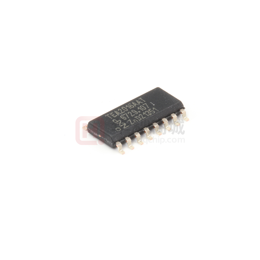
TEA2016AAT
Digital controller for high-efficiency resonant power supply
Rev. 1.2 — 6 April 2020
1
Product data sheet
General description
The TEA2016AAT is a digital configurable LLC and PFC combo controller for highefficiency resonant power supplies. It includes both the LLC controller functionality and
PFC controller operating in DCM and QR mode. The TEA2016AAT enables building a
complete resonant power supply which is easy to design and has a very low component
count. The TEA2016AAT comes in a low profile and narrow body-width SO16 package.
The TEA2016AAT digital architecture is based on a high-speed configurable hardware
state machine ensuring very reliable real-time performance. During the power supply
development, many operation and protection settings of the LLC and PFC controller
can be adjusted by loading new settings into the device to meet specific application
requirements. The configurations can be fully secured to prevent unauthorized copying of
the proprietary TEA2016AAT configuration content.
In contrast to traditional resonant topologies, the TEA2016AAT shows a very high
efficiency at low loads due to the low-power mode. This mode operates in the power
region between continuous switching (also called high-power mode) and burst mode.
Because the TEA2016AAT regulates the output voltage of the system via the primary
capacitor voltage, it has accurate information about the power delivered to the output.
This measured output power defines the mode of operation (burst mode, low-power
mode, or high-power mode). The transition levels of the operating modes can be easily
programmed into the device.
The TEA2016AAT contains all protections like overtemperature protection (OTP),
overcurrent protection (OCP), overvoltage protection (OVP), overpower protection (OPP),
open-loop protection (OLP), and capacitive mode regulation (CMR). Each of these
protections can be configured independently and accurately by programming parameters
inside the device.
The device contains both a low-voltage and high-voltage silicon technology for highvoltage start-up, integrated drivers, level shifter, protections, and circuitry assuring zerovoltage switching.
The TEA2016AAT/TEA1995T combination gives an easy to design, highly efficient, and
reliable power supply, providing 90 W to 500 W, with a minimum of external components.
The system provides a very low no-load input power (< 75 mW; total system including the
TEA2016AAT/TEA1995T combination) and high efficiency from minimum to maximum
load. This power supply meets the efficiency regulations of Energy Star, the Department
of Energy, the Eco-design directive of the European Union, the European Code of
Conduct, and other guidelines. So, any auxiliary low-power supply can be omitted.
�TEA2016AAT
NXP Semiconductors
Digital controller for high-efficiency resonant power supply
2
Features and benefits
2.1 Distinctive features
•
•
•
•
•
•
•
•
Complete functionality of LLC and PFC controller in single small-size SO16 package
Integrated high-voltage start-up
Integrated drivers and high-voltage level shifter (LS)
High-side driver directly supplied from the low-side driver output (patent nr
82059363US01)
Accurate boost voltage regulation
Integrated X-capacitor discharge without additional external components
Power good function
Several parameters can easily be configured, like:
– Operating frequencies to be outside the audible area at all operating modes
– Soft start and soft stop in burst mode, reducing the audible noise
– Accurate transition levels between operation modes (high-power mode/low-power
mode/burst mode)
2.2 Green features
•
•
•
•
Valley/zero voltage switching for minimum switching losses
Extremely high efficiency from low load to high load
Compliant with latest energy saving standards and directives (Energy Star, EuP)
Excellent no-load input power (< 75 mW for TEA2016AAT/TEA1995T combination)
2.3 Protection features
• Independently configurable levels and timers
• All protections can independently be set to latched, safe restart, or latched after several
attempts to restart (Patent 82096505US01)
• Supply undervoltage protection (UVP)
• Overpower protection (OPP)
• Internal and external overtemperature protection (OTP)
• Capacitive mode regulation (CMR)
• Accurate overvoltage protection (OVP)
• Overcurrent protection (OCP)
• Inrush current protection (ICP)
• Brownin/brownout protection
• Disable input
TEA2016AAT
Product data sheet
All information provided in this document is subject to legal disclaimers.
Rev. 1.2 — 6 April 2020
© NXP B.V. 2020. All rights reserved.
2 / 58
�TEA2016AAT
NXP Semiconductors
Digital controller for high-efficiency resonant power supply
3
Applications
•
•
•
•
4
Desktop and all-in-one PCs
LCD television
Notebook adapter
Printers
Ordering information
Table 1. Ordering information
Type number
TEA2016AAT/1
5
Package
Name
Description
Version
SO16
plastic small outline package; 16 leads; body width 3.9 mm
SOT109-1
Marking
Table 2. Marking code
TEA2016AAT
Product data sheet
Type number
Marking code
TEA2016AAT/1
TEA2016AAT
All information provided in this document is subject to legal disclaimers.
Rev. 1.2 — 6 April 2020
© NXP B.V. 2020. All rights reserved.
3 / 58
�TEA2016AAT
NXP Semiconductors
Digital controller for high-efficiency resonant power supply
6
Block diagram
DRAINPFC
DIGITAL CORE AND CONTROL
Valleydet
Vprot(ovp)PFC
SNSBOOST
I
SUPIC
Xcap
discharge
V error
2.5 V
475 V
start-up
PFCOVP
2.63 V
VALLEYDET
disable
0.39 V
LLC DRIVERS
GATEHS
GATEPFC
GATEPFC
GATEHS
GATELS
demag
-10 mV
SNSCURPFC
SUPHS
LS
OCP
GATELS
SWITCHING CONTROL
-0.3 V
Vhs(SNSCAP)
D/A
caph
INTC
capl
OTP
3V
5V
Vmains
Vis(SNSCAP)
12 kΩ
low-power mode
burston
IBI/BO
brownin/brownout
6 kΩ
HB peak/valley
CMR
12 kΩ
FEEDBACK CONTROL
1
:
SNSCAP
D/A
VALLEY /
PEAK
DETECT
+/-
A/D
P
HB
LLC CURRENT SENSE
1
VPOWERGOOD
12 kΩ
OPERATION MODE
LLCOCP
SNSMAINS
+/Plowpwr
= 1.5 V
= 0.1 V
SNSCURLLC
0.96 V
1.2 V
2.4 V
s
q
r
# BURST
CYCLES
SNSFB
GND
aaa-026787
Figure 1. Block diagram
TEA2016AAT
Product data sheet
All information provided in this document is subject to legal disclaimers.
Rev. 1.2 — 6 April 2020
© NXP B.V. 2020. All rights reserved.
4 / 58
�TEA2016AAT
NXP Semiconductors
Digital controller for high-efficiency resonant power supply
7
Pinning information
7.1 Pinning
SNSMAINS
1
16 SNSFB
SNSBOOST
2
15 SNSCURLLC
SNSCURPFC
3
14 SNSCAP
GND
4
GATEPFC
5
GATELS
6
11 HB
HVS
7
10 SUPHS
DRAINPFC
8
IC
13 SUPIC
12 HVS
9 GATEHS
aaa-030882
Figure 2. TEA2016AAT pin configuration (SOT109-1)
7.2 Pin description
Table 3. Pin description
TEA2016AAT
Product data sheet
Symbol
Pin Description
SNSMAINS
1
sense input for mains voltage and external temperature
SNSBOOST
2
sense input for boost voltage; externally connected to resistive divided
boost voltage
SNSCURPFC
3
PFC current sense input
GND
4
ground
GATEPFC
5
PFC MOSFET gate driver output
GATELS
6
LLC low-side MOSFET gate driver output and supply for bootstrap
capacitor
HVS
7
high-voltage spacer. Not to be connected.
DRAINPFC
8
internal HV start-up source also used for X- capacitor discharge, valley
detection, and PFC OVP detection; connected to (PFC) drain voltage
GATEHS
9
LLC high-side MOSFET gate driver output
SUPHS
10
high-side driver supply input; externally connected to bootstrap capacitor
(CSUPHS)
HB
11
low-level reference for high-side driver and input for half-bridge slope
detection; externally connected to half-bridge node HB between the LLC
MOSFETs
HVS
12
high-voltage spacer. Not to be connected.
SUPIC
13
input supply voltage and output of internal HV start-up source; externally
connected to an auxiliary winding of the LLC via a diode or to an external
DC supply
SNSCAP
14
LLC capacitor voltage sense input; externally connected to divider across
LLC capacitor
All information provided in this document is subject to legal disclaimers.
Rev. 1.2 — 6 April 2020
© NXP B.V. 2020. All rights reserved.
5 / 58
�TEA2016AAT
NXP Semiconductors
Digital controller for high-efficiency resonant power supply
TEA2016AAT
Product data sheet
Symbol
Pin Description
SNSCURLLC
15
LLC current sense input; externally connected to the resonant current
sense resistor
SNSFB
16
output voltage regulation feedback sense input; externally connected to
an optocoupler. Output for power good function.
All information provided in this document is subject to legal disclaimers.
Rev. 1.2 — 6 April 2020
© NXP B.V. 2020. All rights reserved.
6 / 58
�TEA2016AAT
NXP Semiconductors
Digital controller for high-efficiency resonant power supply
8
Functional description
8.1 Supply voltages
The TEA2016AAT includes:
• A high-voltage supply pin for start-up (DRAINPFC)
• A general supply to be connected to an external auxiliary winding (SUPIC pin)
• A floating supply for the high-side driver (SUPHS pin)
8.1.1 Start-up and supply voltage
Initially, the capacitor on the SUPIC pin is charged via the DRAINPFC pin. The
DRAINPFC pin is connected to the drain voltage of the PFC MOSFET. Internally,
a high-voltage current source is located between the DRAINPFC and SUPIC pins
(see Figure 3).
PFC
DRAINPFC
Vovp(prot)
OVP_PROT
VALLEYDET
Vstart(SUPIC)
I = lch(SUPIC) = f(temp)
SUPIC
xcap discharge
aaa-026788
Figure 3. HV start-up
The maximum current of the internal current source is limited to Ich(SUPIC). To limit the IC
dissipation, the charge current is reduced when the current source exceeds its maximum
temperature (TSUPICcharger).
When the SUPIC reaches the Vstart(SUPIC) level, it is continuously regulated to
this start level with a hysteresis (Vstart(hys)SUPIC). It activates the current source
between the DRAINPFC and SUPIC pins when the SUPIC voltage drops to below
Vstart(SUPIC) − Vstart(hys)SUPIC. When it exceeds Vstart(SUPIC), it deactivates the switch.
When the start level is reached, it reads the internal MTP (multi-time programmable
memory) and defines the settings.
When the SUPIC voltage drops to below its stop levels, the TEA2016AAT enters the nosupply state. It recharges the SUPIC pin to its start level via the DRAINPFC pin. During
the no-supply state and the reading of the MTP, the LLC and PFC are disabled. When
the settings have been defined, the PFC starts up. When the SNSBOOST reaches the
minimum level Vstart(SNSBOOST), the LLC also starts switching (see Figure 4 and Figure 5).
TEA2016AAT
Product data sheet
All information provided in this document is subject to legal disclaimers.
Rev. 1.2 — 6 April 2020
© NXP B.V. 2020. All rights reserved.
7 / 58
�TEA2016AAT
NXP Semiconductors
Digital controller for high-efficiency resonant power supply
When start-up is complete and the LLC controller is operating, the LLC transformer
auxiliary winding supplies the SUPIC pin. In this operational state, the HV start-up source
is disabled.
When the system enters the protection mode, it cannot be supplied via the auxiliary
winding. So, the SUPIC pin is regulated to Vstart(SUPIC) via the DRAINPFC pin.
During the non-switching period of the burst mode, the SUPIC is regulated to the
Vlow(SUPIC) when SUPIC drops to below this level. It regulates the voltage with a
hysteresis of Vlow(hys)SUPIC. In this way, the system avoids that the SUPIC undervoltage
protection (Vuvp(SUPIC)) is triggered because of a long non-switching period in burst mode.
The DRAINPFC pin is also used for valley detection, for X-capacitor discharge, and for
providing a second PFC OVP protection.
ISNSMAINS
Ibi(SNSMAINS)
on
supic_charge
ISUPIC
VSUPIC
off
Ich(SUPIC)
Vstart(SUPIC)
Vstart(hys)(SUPIC)
Vstart(SNSBOOST)
SNSBOOST
Vout
ISNSFB > Ivoutreg(SNSFB)
mode of operation
No Supply
Measure lmains
PFC startup
Readout settings
LLC startup
Operating
aaa-026789
Figure 4. Start-up sequence and normal operation
TEA2016AAT
Product data sheet
All information provided in this document is subject to legal disclaimers.
Rev. 1.2 — 6 April 2020
© NXP B.V. 2020. All rights reserved.
8 / 58
�TEA2016AAT
NXP Semiconductors
Digital controller for high-efficiency resonant power supply
VSUPIC < Vstop(SUPIC)
No supply
VSUPIC > Vstart(SUPIC)
PFC disabled
Readout settings
all settings defined
LLC disabled
Measure
lmains
SUPIC regulated
via DRAINPFC
VSNSBOOST > Vscp(start)
PFC start-up
VSNSBOOST > Vstart(SNSBOOST)
LLC start-up
ISNSFB > Ivo(reg)SNSFB
Operating
aaa-026791
Figure 5. LLC controller flow diagram
8.1.2 High-side driver floating supply (SUPHS pin)
As the voltage range on the SUPIC pin exceeds that of the maximum external MOSFETs
gate-source voltage, the external bootstrap capacitor CSUPHS cannot directly be supplied
from the SUPIC.
To provide an external supply for the high-side driver without the need of additional
external components, the GateLS output is designed such that it can drive the lowside MOSFET and supply the high-side MOSFET (patent number 82059363US01;
see Figure 6).
TEA2016AAT
Product data sheet
All information provided in this document is subject to legal disclaimers.
Rev. 1.2 — 6 April 2020
© NXP B.V. 2020. All rights reserved.
9 / 58
�TEA2016AAT
NXP Semiconductors
Digital controller for high-efficiency resonant power supply
DSUPHS
GATELS
ID(SUPHS)
SUPHS
CSUPHS
GATEHS
S2
LS
HB
VHB
IC
LM
GATELS
S1
CR
VGateHS - VHB
SUPIC
CSUPIC
VGateLS
aaa-027835
aaa-026790
a. Curves
b. Circuit
Figure 6. High-side driver supply
The external bootstrap buffer capacitor CSUPHS supplies the high-side driver. The
bootstrap capacitor is connected to the low-side driver supply, the GATELS pin, and the
half-bridge node (HB) via an external diode (DSUPHS). When GATELS is active high and
the HB node is pulled low, CSUPHS is charged.
Careful selection of the appropriate diode minimizes the voltage drop between the
GATELS and SUPHS pins, especially when large MOSFETs and high switching
frequencies are used. A great voltage drop across the diode reduces the gate drive of the
high-side MOSFET.
TEA2016AAT
Product data sheet
All information provided in this document is subject to legal disclaimers.
Rev. 1.2 — 6 April 2020
© NXP B.V. 2020. All rights reserved.
10 / 58
�TEA2016AAT
NXP Semiconductors
Digital controller for high-efficiency resonant power supply
8.2 LLC system regulation
A typical resonant controller regulates the output power by adapting the operating
frequency.
Vboost
trafo model
GATEHS
LS
D2
Vout
Ls
Lm
FREQUENCY CONTROL
GATELS
frequency
D1
fmax
Cr
fmin
SUPREG
VSNSFB
SNSFB
SNSBURST
3.5 V
aaa-034987
Figure 7. Resonant frequency controller
If the requested power at the outputs decreases, the output voltage of the LLC converter
exceeds the targeted regulation level (12 V or 19.5 V typical), the optocurrent increases,
and the voltage at the SNSFB decreases (see Figure 7). The resonant controller then
increases the frequency according to its internal frequency control curve. Because of the
higher frequency, the power to the output is reduced and the output voltage decreases.
If the output voltage becomes too low, the controller lowers the system frequency,
increasing the output power. In this way, the system regulates the output power to the
required level.
As a small change in frequency gives a significant change in output power, frequency
control has a high gain of the control loop. To increase the efficiency at low loads, most
converters switch to burst mode as soon as the output power is below a minimum
level. The burst mode level is mostly derived from the voltage on the SNSFB pin. For
a frequency controlled resonant converter, it implies that the burst mode is entered
at a certain frequency instead of at a certain load. A small variation of the resonant
components results in a significant variation in power level at which the burst mode is
activated.
In the TEA2016AAT, the control mechanism is different. The advantage is a constant
gain of the control loop and a burst mode which is derived from the output power. The
TEA2016AAT does not regulate the output power by adjusting the frequency but by the
voltage across the primary capacitor.
The input power (related to the output power) of a resonant converter can be calculated
with Equation 1:
TEA2016AAT
Product data sheet
All information provided in this document is subject to legal disclaimers.
Rev. 1.2 — 6 April 2020
© NXP B.V. 2020. All rights reserved.
11 / 58
�TEA2016AAT
NXP Semiconductors
Digital controller for high-efficiency resonant power supply
(1)
Equation 1 shows that the input power has a linear relationship with the capacitor voltage
difference ΔVCr.
Figure 8 shows an alternative explanation of the linear relationship between the input
power and the energy stored in the resonant capacitor.
Vboost
Vout
GATEHS
HB
Ls
Lm
GATELS
Cr
aaa-034988
Figure 8. Linear relationship between input power and energy stored in Cr
When the high-side switch is on, a primary current is flowing through the transformer
and resonant capacitor Cr as indicated by the red line. Half the energy the input delivers
is transferred to the output. The other half charges resonant capacitor Cr. The voltage
across the resonant capacitor increases.
When the high-side switch is off and the low-side switch is on, the energy which is stored
in resonant capacitor Cr is transferred to the output and its voltage decreases. In this
way, the linear relationship between the increase of the resonant capacitor voltage and
the output power can be seen.
Although the TEA2016AAT uses the primary capacitor voltage as a regulation parameter,
all application values, like the resonant inductances, resonant capacitor, and primary
MOSFETs remain unchanged compared to a frequency controlled LLC converter. A
secondary TL431 circuitry in combination with an optocoupler connected to the primary
SNSFB pin continuously regulates the output voltage.
TEA2016AAT
Product data sheet
All information provided in this document is subject to legal disclaimers.
Rev. 1.2 — 6 April 2020
© NXP B.V. 2020. All rights reserved.
12 / 58
�TEA2016AAT
NXP Semiconductors
Digital controller for high-efficiency resonant power supply
8.2.1 Output power regulation loop
Figure 9 shows the output power regulation loop of Vcap control as used by the
TEA2016AAT. Figure 10 shows a corresponding timing diagram.
Vboost
IC
GATEHS
LS
trafo model
D2
Vout
Ls
Lm
Vcap CONTROL
VSNSCAP
burst
GATELS
D1
Vhs(SNSCAP)
Vls(SNSCAP)
Iburst
q
s
qn r
ISNSFB
Vhs(SNSCAP)
SNSCAP
Vls(SNSCAP)
ISNSFB
Cr
SNSFB
2.5 V
aaa-034989
Figure 9. Regulation loop Vcap control
Iload
Ireg(SNSFB) (80 µA)
ISNSFB
Vhs(SNSCAP)
VSNSCAP
Vls(SNSCAP)
t
GATEHS
GATELS
t1
t2
aaa-031214
Figure 10. Timing diagram of the regulation loop
When the divided resonant capacitor voltage (VSNSCAP) exceeds the capacitor voltage
high level (Vhs(SNSCAP)), the high-side MOSFET is switched off (see Figure 10 (t1)). After
a short delay, the low-side MOSFET is switched on. Because of the resonant current, the
resonant capacitor voltage initially increases further but eventually drops.
TEA2016AAT
Product data sheet
All information provided in this document is subject to legal disclaimers.
Rev. 1.2 — 6 April 2020
© NXP B.V. 2020. All rights reserved.
13 / 58
�TEA2016AAT
NXP Semiconductors
Digital controller for high-efficiency resonant power supply
When the divided capacitor voltage (VSNSCAP) drops to below the capacitor voltage low
level (Vls(SNSCAP)), the low-side MOSFET is switched off (see Figure 10 (t2)). After a
short delay, the high-side MOSFET is switched on. Figure 10 shows that the switching
frequency is a result of this switching behavior. In a frequency controlled system, the
frequency is a control parameter and the output power is a result. The TEA2016AAT
regulates the power and the frequency is a result.
The difference between the high and low capacitor voltage level is a measure of the
delivered output power. The value of the primary optocurrent, defined by the secondary
TL431 circuitry, determines the difference between the high and low capacitor voltages.
Figure 10 also shows the behavior at a transient. If the output load increases, the current
pulled out of the SNSFB pin decreases. The result is that the TEA2016AAT increases
the high-level capacitor voltage and lowers the low-level capacitor voltage. According to
Equation 1 in Section 8.2, the output power increases and eventually the output voltage
increases to its regulation level.
To minimize no-load input power of the system, the primary current into the optocoupler
is continuously regulated to 85 μA (see Section 8.4).
8.2.2 Output voltage start-up
The system controls the output power by regulating the primary VCr (see Section 8.2).
When the system is in regulation and the output voltage is stabilized, a small change in
ΔVCr corresponds to a small change in the output current (see Equation 2).
(2)
However, before start-up, when the output voltage is around zero, a small capacitor
voltage increase (ΔVCr) corresponds to a substantial output current increase. So, at startup, the divided ΔVCr voltage (ΔVSNSCAP) is slowly increased from a minimum value to the
regulation level. As a result, the system starts up at a higher frequency.
While the system increases the ΔVSNSCAP, it continuously monitors the primary current
via the SNSCURLLC pin. When the voltage at this pin exceeds the Vlmtr(ocp) level,
increasing the ΔVSNSCAP is on hold until the voltage at the SNSCURLLC pin drops
below the Vlmtr(ocp) level again (see Figure 11). The output current is regulated and its
voltage shows a nice ramp during start-up. It also avoids that during startup the OCP
(OverCurrent Protection) is triggered. In this way, the LLC converter behaves like a
limited current source during start-up.
TEA2016AAT
Product data sheet
All information provided in this document is subject to legal disclaimers.
Rev. 1.2 — 6 April 2020
© NXP B.V. 2020. All rights reserved.
14 / 58
�TEA2016AAT
NXP Semiconductors
Digital controller for high-efficiency resonant power supply
VSNSCAP
VSNSCURLLC
Vlmtr(ocp)
VOUT
aaa-026792
Figure 11. LLC start-up behavior
8.3 Modes of operation
Figure 12 shows the control curve between the output power and the voltage difference
between the high and low capacitor voltage levels.
VSNSCAP
VSNSCAP control
Vhs(SNSCAP)
VSNSCAP
Vls(SNSCAP)
burst mode
low-power mode
high-power mode
Pt(lp)
Pout(max)
aaa-026793
Figure 12. TEA2016AAT control curve
When the output power (Pout) is at its maximum, the low capacitor voltage level
(Vls(SNSCAP)) is at its minimum and the high capacitor voltage (Vhs(SNSCAP)) is at its
maximum level. According to Equation 1 in Section 8.2, the maximum ΔVSNSCAP
(Vhs(SNSCAP) − Vls(SNSCAP)), which is the divided ΔVCr voltage, corresponds to the
maximum output power.
When the output load decreases, the ΔVSNSCAP voltage decreases. As a result, the
output power decreases and the output voltage is regulated. This mode is called highpower mode. Figure 10 shows a timing diagram of the system operating in high-power
mode.
TEA2016AAT
Product data sheet
All information provided in this document is subject to legal disclaimers.
Rev. 1.2 — 6 April 2020
© NXP B.V. 2020. All rights reserved.
15 / 58
�TEA2016AAT
NXP Semiconductors
Digital controller for high-efficiency resonant power supply
When the output power drops to below the transition level (Pt(lp)), the system enters the
low-power mode. The Pt(lp) level can be initialized via the MTP.
To compensate for the non-switching period in low-power mode, also called hold period,
ΔVSNSCAP is initially increased at entering the low-power mode (see Section 8.3.2). In
low-power mode, the output power is regulated by adapting ΔVSNSCAP, until it reaches a
minimum. The system then enters the burst mode (see Section 8.3.3).
8.3.1 High-power mode
In high-power mode, the system operates as described in Section 8.2.1. Figure 13 shows
a flow diagram of the high-power mode.
System off
GATELS = on/GATEHS = off
t > ton(min)
VSNSCAP < Vls(SNSCAP)
lprim < -locp
lprim > -lreg(capm)
t > ton(max)
GATELS = off/GATEHS = off
t > tno(min)
lprim ≤ 0
End of HB slope
t > tno(max)
GATELS = off/GATEHS = on
t > ton(min)
VSNSCAP > Vhs(SNSCAP)
lprim > locp
lprim < lreg(capm)
t > ton(max)
GATELS = off/GATEHS = off
t > tno(min)
lprim ≤ 0
End of HB slope
t > tno(max)
explanation flow diagram
settings
exit condition 1
exit condition 2a
exit condition 2b
exit condition 2c
exit condition 2d
settings: actions taken when the system is in this state
exit condition: exit condition 1 has to be fulfilled and one of
the exit conditions 2x
aaa-017758
Figure 13. High-power mode flow diagram
TEA2016AAT
Product data sheet
All information provided in this document is subject to legal disclaimers.
Rev. 1.2 — 6 April 2020
© NXP B.V. 2020. All rights reserved.
16 / 58
�TEA2016AAT
NXP Semiconductors
Digital controller for high-efficiency resonant power supply
Initially, GATELS is on and GATEHS is off. The external bootstrap buffer capacitor
(CSUPHS) is charged via the GATELS pin and an external diode. The system remains in
this state for at least the minimum on-time (ton(min)) of GATELS. Before entering the next
state, one of the following conditions must be fulfilled:
•
•
•
•
The VSNSCAP voltage drops to below the minimum VSNSCAP voltage (Vls(SNSCAP))
The measured current exceeds the OCP level (see Section 8.6.15)
The system is close to capacitive mode (see Section 8.6.14)
The maximum on-time (ton(max)), a protection that maximizes the time the high-side or
low-side MOSFET is kept on, is exceeded.
In the next state, to avoid false detection of the HB peak voltage, the system waits until
the minimum non-overlap time (tno(min)) is exceeded. When it is exceeded, the system
starts to detect the end (= peak voltage) of the HB node. When it detects the peak of
the HB node and the measured resonant current is negative (or zero), it enters the next
state.
If the system does not detect a peak at the HB node, it also enters the next state when
the maximum non-overlap time (tno(max)) is exceeded under the condition of a negative
(or zero) resonant current.
Finally, the third and fourth states (see Figure 13) describe the GATEHS and GATEHS to
GATELS transition criteria which are the inverse of the first two states.
8.3.2 Low-power mode
At low loads, the operating frequency of a resonant converter increases. As a result,
the magnetization and switching losses increase. For this reason, the efficiency of a
resonant converter drops at low loads. A newly introduced low-power mode ensures high
efficiency at lower loads as well.
When the output power drops to below the Pt(lp) level, the system enters the low-power
mode (see Figure 12 and Figure 14). It continues switching for 3 half-cycles (low-side,
high-side, low-side) with an MTP selectable duty cycle. To ensure a constant output
power level, it increases the energy per cycle (Vhs(SNSCAP) − Vls(SNSCAP)) at the same
time.
TEA2016AAT
Product data sheet
All information provided in this document is subject to legal disclaimers.
Rev. 1.2 — 6 April 2020
© NXP B.V. 2020. All rights reserved.
17 / 58
�TEA2016AAT
NXP Semiconductors
Digital controller for high-efficiency resonant power supply
Iload
high-power mode
low-power mode
Vhs(SNSCAP)
VSNSCAP
VSNSCAP
Vls(SNSCAP)
3 half-cycles
hold
period
tlp
ID1
ID2
aaa-017765
Figure 14. Timing diagram transition high-power mode to low-power mode
As the system continuously tracks the primary capacitor voltage, it knows exactly when
to enter the "hold" period. It can also continue again at exactly the correct voltage and
current levels of the resonant converter. In this way, a "hold" period can be introduced
which reduces the magnetization and switching losses without any additional losses. The
currents ID1 and ID2 (see Figure 14) are the secondary currents through diodes D1 and
D2 (see Figure 25).
When in low-power mode the output power is further reduced, the amount of energy per
cycle (= ΔVSNSCAP) is reduced and the duty cycle remains the same (see Figure 15).
When in low-power mode the system reaches the programmable minimum energy per
cycle (= ΔVSNSCAP), it enters burst mode.
TEA2016AAT
Product data sheet
All information provided in this document is subject to legal disclaimers.
Rev. 1.2 — 6 April 2020
© NXP B.V. 2020. All rights reserved.
18 / 58
�TEA2016AAT
NXP Semiconductors
Digital controller for high-efficiency resonant power supply
Iload
Vhs(SNSCAP)
VSNSCAP
Vls(SNSCAP)
ID1
ID2
aaa-017766
Figure 15. Low-power mode: Lowering the energy-per-cycle (ΔVSNCAP)
8.3.3 Burst mode
In burst mode, the system alternates between operating in low-power mode and an
extended hold state (see Figure 16). Because of this additional extended hold period, the
magnetization and switching losses are further reduced. So, the efficiency of the system
is increased.
Figure 16 shows all operating frequencies outside the audible area. The minimum lowpower frequency can be set with a parameter. Within a low-power period, the system is
switching at the resonant frequency of the converter, which is typically between 50 kHz
and 200 kHz.
low-power
hold
hold
low-power
hold
ISNSFB
106 µA
burst-on
Isec
tlp
Tburst
aaa-017768
Figure 16. Burst mode
TEA2016AAT
Product data sheet
All information provided in this document is subject to legal disclaimers.
Rev. 1.2 — 6 April 2020
© NXP B.V. 2020. All rights reserved.
19 / 58
�TEA2016AAT
NXP Semiconductors
Digital controller for high-efficiency resonant power supply
8.3.3.1 Frequency regulation
The burst frequency (1 / tburst) is continuously regulated to a predefined value, which can
be set with a parameter. As both the low power and burst frequency can be accurately
set with parameters, they can be chosen such that they are outside the audible area. Isec
is the secondary current flowing through either diode D1 or D2 (see Figure 25).
When the primary optocurrent (ISNSFB) drops to below Istart(burst) (100 μA), a new
burst-on period is started. The end of the burst-on period depends on the calculated
number of low-power cycles. The number of low-power cycles within a burst-on is
continuously adjusted so that the burst period is at least the period defined by the setting
(see Figure 17).
Iload
ISNSFB
106 µA
burst-on
Isec
Tburst
Vstart(SNSBOOST)
-
off
-
-
off
-
OVP SUPIC
output overvoltage LLC and PFC are either
protection;
latched or safe restart
measured via the
SUPIC pin
off
off
Y
CMR
capacitive mode
regulation
system ensures that mode of
operation is inductive
-
-
Y
OCP
overcurrent
protection
switch off cycle-by-cycle;
After several consecutive
cycles, LLC and PFC are
either latched or safe restart
off
off
Y
STARTUP MAX
maximum start-up LLC and PFC are either
time
latched or safe restart
off
off
Y
OPP
overpower
protection
off
off
Y
[1]
LLC and PFC are either
latched or safe restart
Selectable via a parameter at the MTP.
When the system is in a latched or safe restart protection, the SUPIC voltage is regulated
to its start level via the DRAINPFC pin.
8.6.1 Undervoltage protection SUPIC
When the voltage on the SUPIC pin is below its undervoltage level Vuvp(SUPIC), both the
PFC and LLC converter stop switching. The capacitors at the SUPIC pin are recharged
via the DRAINPFC pin.
When the SUPIC supply voltage exceeds its start level, the system restarts.
8.6.2 MTP fail
When, at start-up, the SUPIC reaches the start level, the system reads the parameters
from the internal MTP. If reading the MTP failed, the system retries reading the MTP until
it succeeds. During this time, the PFC and LLC remain off. The SUPIC is regulated to the
Vstart(SUPIC) level.
8.6.3 Internal overtemperature protection (OTP)
An accurate internal temperature protection is provided in the circuit. When the junction
temperature exceeds the thermal shutdown temperature, the PFC and the LLC stop
switching.
The response of the internal OTP follows the setting of the external OTP. It can be either
latched or safe restart.
TEA2016AAT
Product data sheet
All information provided in this document is subject to legal disclaimers.
Rev. 1.2 — 6 April 2020
© NXP B.V. 2020. All rights reserved.
26 / 58
�TEA2016AAT
NXP Semiconductors
Digital controller for high-efficiency resonant power supply
8.6.4 Brownin/brownout and external overtemperature protection
On the TEA2016AAT, the mains measurement and external temperature are combined
at the SNSMAINS pin (see Figure 21).
mains-L
mains-N
20 MΩ
Intc
ntc measurement
SNSMAINS
A/D
5V
DIGITAL
CONTROL
mains resistor value
3V
RNTC
10 nF
6 kΩ
12 kΩ
aaa-030887
a. Circuit
mains-L
mains-N
VSNSMAINS
ISNSMAINS 0
t1
t2
aaa-030888
b. Timing diagram
Figure 21. Mains and external OTP management
The TEA2016AAT continuously measures the SNSMAINS voltage via an A/D converter
and waits until it detects a peak (t1). This peak value is internally stored and used as an
input for the brownout/brownin detection and the mains compensation.
The TEA2016AAT continuously measures the mains voltage. There is an internal counter
that counts the number of peaks. During one out of 4 peaks, it measures the external
temperature.
TEA2016AAT
Product data sheet
All information provided in this document is subject to legal disclaimers.
Rev. 1.2 — 6 April 2020
© NXP B.V. 2020. All rights reserved.
27 / 58
�TEA2016AAT
NXP Semiconductors
Digital controller for high-efficiency resonant power supply
8.6.5 Short-circuit protection/fast disable
The PFC and LLC do not start switching until the voltage on the SNSBOOST pin exceeds
Vscp(start). This function acts as short circuit protection for the boost voltage.
When the SNSBOOST pin is shorted to ground or the SNSBOOST pull-up resistor is
disconnected, this protection inhibits switching.
This function can also be used as a fast disable. If this pin is shorted to ground via
an external MOSFET, the system either stops switching or enters the protection
mode followed by safe restart or latched protection. In this way, an additional external
protection can be added.
8.6.6 Brownout mains
On the TEA2016AAT, the mains measurement and external temperature are combined
at the SNSMAINS pin.
To prevent the PFC from operating at very low mains input voltages, the PFC stops
switching when the measured mains voltage drops to below the brownout level. When
the mains voltage exceeds the brownin level, the PFC restarts with a soft start. To avoid
that the system is interrupted during a short mains interruption, a delay can be set before
the brownout function is active.
The external resistor, which is connected between the mains input voltage, can be either
20 MΩ or 10 MΩ. These values can be set with a parameter.
Typically, only the PFC stops switching and the LLC continues at a brownout. Due to
the large PFC bulk capacitor, the LLC can continue for a long period while the mains is
already disconnected. So the option to stop the LLC at a brownout after a given delay
can be selected with a parameter.
8.6.7 Overvoltage protection (SNSBOOST pin)
To prevent output overvoltage during load steps and mains transients, a PFC output
overvoltage protection circuit is built in. When the voltage on the SNSBOOST pin
exceeds the Vovp(stop) level, switching of the power factor correction circuit is inhibited.
When the SNSBOOST pin voltage drops to below the regulation level (Vreg(SNSBOOST))
again, the switching of the PFC recommences. The IC always restarts with a soft start.
When an OVP at the SNSBOOST is detected for a minimum period (can be set using a
parameter), the LLC can also be disabled.
8.6.8 Overvoltage protection (DRAINPFC pin)
To prevent output overvoltage of the PFC due to a disturbed SNSBOOST pin, an
additional PFC output overvoltage protection is available. This overvoltage protection is
measured via the DRAINPFC pin.
The DRAINPFC overvoltage protection level and the delay before it enters the protection
state can be set with parameters.
The DRAINPFC overvoltage protection can be a latched, a safe restart, or a latched after
safe restart protection.
TEA2016AAT
Product data sheet
All information provided in this document is subject to legal disclaimers.
Rev. 1.2 — 6 April 2020
© NXP B.V. 2020. All rights reserved.
28 / 58
�TEA2016AAT
NXP Semiconductors
Digital controller for high-efficiency resonant power supply
8.6.9 Overcurrent protection (SNSCURPFC pin)
The PFC current is measured via an external sense resistor (Rsense) connected to the
SNSCURPFC pin. If the voltage drops to below Vocp(PFC), the PFC MOSFET is turned off.
It resumes switching at the next cycle. To ensure that the OCP level is not exceeded due
to disturbance caused by a turn on of the PFC MOSFET, the OCP level is blanked for
300 ns (tleb).
8.6.10 PFC coil short protection (SNSCURPFC pin)
When the overcurrent protection is continuously triggered, the cause may be a shorted
PFC coil. To avoid overheating, the system enters the protection state when the OCP is
continuously triggered for 100 ms (tocp(PFC)). The PFC and LLC converters stop switching
and a restart follows.
8.6.11 Undervoltage protection SUPHS
To ensure a minimum drive voltage at the high-side driver output (GATEHS), this driver is
kept off when its voltage is below the minimum level (VSUPHS < Vrst(SUPHS)).
8.6.12 Undervoltage protection boost
The PFC output voltage is measured via a resistive divider connected to the
SNSBOOST pin. The voltage at the SNSBOOST pin must exceed the start level
(VSNSBOOST > Vstart(SNSBOOST)) before the LLC converter is allowed to start switching.
When the system is operating and the voltage at the SNSBOOST pin drops to below the
minimum level (VSNSBOOST < Vuvp(SNSBOOST)), the LLC converter stops switching. When it
exceeds the start level, it restarts.
8.6.13 Overvoltage protection
When the voltage at the SUPIC pin exceeds the Vovp(SUPIC) level for tovp(SUPIC), the OVP
protection is triggered. The voltage at the SUPIC pin is continuously monitored via an
internal ADC converter.
The OVP protection level (VOVP(SUPIC)) and the OVP delay time can be selected with a
parameter.
The OVP function can also be disabled.
8.6.14 Capacitive mode regulation (CMR)
The TEA2016AAT has a capacitive mode regulation (CMR) which ensures that the
system is always operating in inductive mode and avoids operation in capacitive mode.
At lower input voltage or higher output power and depending on the resonant design, the
resonant current can already approach zero before the capacitor voltage reaches the
regulation level.
When the resonant current has changed polarity before the switches are turned off and
the other switch is turned on, hard switching occurs. This event is called capacitive mode.
To avoid that it operates in capacitive mode, the system also switches off the high-side/
low-side switch when the resonant current approaches zero.
TEA2016AAT
Product data sheet
All information provided in this document is subject to legal disclaimers.
Rev. 1.2 — 6 April 2020
© NXP B.V. 2020. All rights reserved.
29 / 58
�TEA2016AAT
NXP Semiconductors
Digital controller for high-efficiency resonant power supply
Figure 22 shows the signals that occur when a resonant converter is switching in
CMR mode. At t1 (and also at t3), the low-side switch is on while the resonant current
approaches zero before VSNSCAP reaches Vls(SNSCAP). At t2, the resonant current is
also close to changing polarity while the divided capacitor voltage (VSNSCAP) has not
reached the Vhs(SNSCAP) level yet. To avoid a turn-off of the high-side switch at a negative
current or the low-side at a positive current, the system also turns off the high-side/lowside switch when the primary current approaches zero. So at t2, the high-side switch
is turned off because the primary current is close to zero. At t3 (and also at t1), the lowside switch is turned off, although VSNSCAP did not reach the regulation level (Vls(SNSCAP))
yet. The primary current is measured via an external sense resistor connected to the
SNSCURLLC pin. The capacitive mode protection levels are Vreg(capm) (−100 mV and
+100 mV, respectively). These protection levels can be adjusted with a parameter.
In this mode, the amount of output power is reduced and the output voltage decreases.
The TEA2016AAT does not enter a so-called "capacitive mode protection", but avoids
this mode of operation.
GATEHS
GATELS
HB
Vhs(SNSCAP)
VSNSCAP
Vls(SNSCAP)
Iprim
Vreg(capm)
0
Vreg(capm)
t0
t1
t2
t3
aaa-017772
Figure 22. Near capacitive mode switching
TEA2016AAT
Product data sheet
All information provided in this document is subject to legal disclaimers.
Rev. 1.2 — 6 April 2020
© NXP B.V. 2020. All rights reserved.
30 / 58
�TEA2016AAT
NXP Semiconductors
Digital controller for high-efficiency resonant power supply
8.6.15 Overcurrent protection
The system measures the primary current continuously via a sense resistor connected to
the SNSCURLLC pin. If the measured voltage exceeds the fixed overcurrent level (Vocp),
the corresponding switch (GATELS/GATEHS) is turned off, but the system continuous
switching. In this way, the primary current is limited to the OCP level.
The OCP level can be adjusted via the external sense resistor.
If the OCP is continuously triggered for an adjustable time, the system enters the OCP
protection state. The OCP protection state can also be disabled. However, the primary
current is always limited to the OCP level.
8.6.16 Maximum start-up time
Initially, the PFC starts switching at start-up. When the PFC output voltage exceeds a
minimum level, the LLC starts switching as well.
If the output voltage of the LLC is not in regulation within an adjustable time after the PFC
has started switching, the maximum start-up time protection is triggered.
The maximum start-up time can be set with parameter “Maximum start-up time”. If this
protection is triggered, the system is latched or does a safe restart, which follows the
setting of the OPP.
8.6.17 Overpower protection
For the overpower protection, three levels can be set:
• Absolute maximum output power, which is the highest output power level.
When the output power exceeds this maximum level, it is limited cycle-by-cycle. If the
output power exceeds this maximum, the output voltage decreases.
The maximum output power can be set to a percentage of the rated output power.
• A first overpower level, which is below the maximum output power level.
When the output power exceeds this power level, a timer is started. When this timer
exceeds a predefined value, the system enters the protection state. Both PFC and LLC
are switched off.
This power level can be set to a predefined level below the selected maximum output
power. So, if the maximum output power is set to 170 % and this first overpower level is
set to −20 %, the timer is started at 150 % of the rated output power.
The timer of the first overpower level can also be set. The first overpower level can also
be disabled.
• A second overpower level, which is typically below the first overpower level.
When the output power exceeds this power level, a timer is started. When this timer
exceeds a predefined value, the system enters the protection state. PFC and LLC are
switched off.
This power level can be set to a predefined level below the selected maximum output
power. So, if the output power is set to 170 % and this second overpower level is set to
−50 %, the timer is started at 120 % of the rated output power.
The timer of the second overpower level can be set to a predefined level. The second
overpower level can also be disabled.
The overpower function can be either latched or safe restart. Section 8.6.18 describes
this function.
TEA2016AAT
Product data sheet
All information provided in this document is subject to legal disclaimers.
Rev. 1.2 — 6 April 2020
© NXP B.V. 2020. All rights reserved.
31 / 58
�TEA2016AAT
NXP Semiconductors
Digital controller for high-efficiency resonant power supply
8.6.18 Latched, safe restart, or latched after safe restart
When a protection is selected to be latched, the system stops switching when
this protection is triggered. The system only restarts after a fast latch reset
(see Section 8.6.19) or when the SUPIC supply voltage drops below the UVP level.
When selecting “latched after safe restart”, a protection is initially a safe restart
protection. If the failure occurs again within a specific time, it latches eventually.
latched after saferestart
OVP
latched
protection
5 sec
restart counter
0
1
2
3
0
1
2
3
4
aaa-030889
Figure 23. Latched after safe restart
Figure 23 shows an example of when the OVP is set to latched after safe restart. Initially
at an OVP, the system restarts. An internal counter is then set to ‘1’. If the protection is
triggered again after the safe restart, the counter is increased. If the counter reaches
the number as set with a parameter, the system latches. If the protection is not triggered
within 5 seconds, the counter is reset.
When a protection is selected to be safe restart, the system continuously restarts after a
predefined period. This safe restart time is the same for all protection functions. It can be
set with a parameter.
8.6.19 Fast latch reset
If a protection is triggered, the system enters the protection state. Especially when the
protection is latched, this function is inconvenient during production tests. So, when the
mains voltage is below the brownout level for a specified time, the system also restarts.
This time can be set with a parameter.
TEA2016AAT
Product data sheet
All information provided in this document is subject to legal disclaimers.
Rev. 1.2 — 6 April 2020
© NXP B.V. 2020. All rights reserved.
32 / 58
�TEA2016AAT
NXP Semiconductors
Digital controller for high-efficiency resonant power supply
8.7 Power good function
The TEA2016AAT provides a power good function via the SNSFB pin.
FEEDBACK CONTROL
1
:
1
power level
SUPIC
VPOWERGOOD
12 kΩ
SNSFB
POWERGOOD
aaa-027838
aaa-027837
a. Primary side
b. Secondary side
Figure 24. Power good function
The primary function of the SNSFB pin is to regulate the output voltage via an
optocoupler. So, it measures the current that is drawn from the SNSFB. Via an internal
12 kΩ resistor, it regulates the output power. The output power regulation is independent
of the voltage level of the SNSFB pin. So, if the system is about to stop operating, the
voltage level at the SNSFB pin is used to indicate; a so-called power good signal. The
voltage at the SNSFB pin can be used to generate a secondary power good signal using
an external MOSFET and an optocoupler.
At start-up, the SNSFB voltage is at a high level, pulling down the secondary power good
signal. As soon as the system enters the operating state (see Figure 5), the SNSFB goes
low. The external power good signal becomes active high.
The SNSFB voltage becomes active high, lowering the secondary power good signal
when:
•
•
•
•
The voltage on the SNSBOOST pin drops to below Vdet(SNSBOOST) (1.75 V)
The OPP counter is close to its end value
The converter is about to stop due to an OTP protection
When the LLC converter is about to stop due to a mains brownout when this function is
enabled
To avoid any disturbance of the regulation loop, the increase and decrease of the SNSFB
voltage is in alignment with a predefined ramp.
When the system enters protection mode (OVP, OCP, or UVP), it pulls high the SNSFB
pin and stops switching immediately.
TEA2016AAT
Product data sheet
All information provided in this document is subject to legal disclaimers.
Rev. 1.2 — 6 April 2020
© NXP B.V. 2020. All rights reserved.
33 / 58
�TEA2016AAT
NXP Semiconductors
Digital controller for high-efficiency resonant power supply
8.8 Settings
The TEA2016AAT has an internal MTP at which different settings can be programmed.
Disclaimer:
The MTP parameter settings can be changed using the “Ringo” GUI software of NXP
Semiconductors. Before the user can change any MTP parameters using the GUI, the
terms and conditions in the start-up pop-up screen must be accepted.
8.8.1 General settings
8.8.1.1 Protection register
When the TEA2016AAT triggers a protection, it can be read which protection was
triggered. Even when the root cause of the protection is solved and the converter
continues switching, the information about the protection remains until the software
program (GUI) clears it.
8.8.1.2 Supply start level
The SUPIC start level can be selected between 12 V and 19 V. Typically, a level of 19 V
is selected. When the TEA2016AAT is externally supplied, for instance via a standby
supply, the lower start level of 12 V can be used.
8.8.1.3 Read lock
Normally, the software tool can read all the programmed settings. This option can be
used to verify the correct settings or for failure analyses.
However, once in production, enabling the "Read lock" bit can protect the parameters.
Then it is not possible anymore to read the MTP content. It can however still be reset to
the default values and also clear the read lock parameter.
8.8.1.4 Write lock
To avoid that the MTP content (accidentally) gets overwritten, a write-lock bit can be set.
It can, however, still be reset to the default values and clear the write lock parameter.
8.8.2 PFC settings
8.8.2.1 Soft-start time
For the soft-start time of the PFC, the following periods can be selected: 2 ms, 4 ms,
6 ms, or 8 ms.
8.8.2.2 Active X-capacitor discharge
When the TEA2016AAT detects that the mains is disconnected, the X-capacitor
discharge is activated after a delay of td(dch)Xcap. The following delays can be selected:
100 ms, 200 ms, and 400 ms. This function can also be disabled.
8.8.2.3 Mains measurement impedance
To realize a low no-load input power level, the external resistor connected to the
SNSMAINS pin for measuring the mains input voltage is typically 20 MΩ.
TEA2016AAT
Product data sheet
All information provided in this document is subject to legal disclaimers.
Rev. 1.2 — 6 April 2020
© NXP B.V. 2020. All rights reserved.
34 / 58
�TEA2016AAT
NXP Semiconductors
Digital controller for high-efficiency resonant power supply
However, some applications request a maximum resistance of 10 MΩ. With this bit,
10 MΩ or 20 MΩ can be selected for the external resistor without affecting the mains
voltage-related levels like brownin and brownout.
8.8.2.4 Burst mode: Output voltage ripple
When the PFC enters burst mode, it stops switching when the SNSBOOST voltage,
which reflects the PFC output voltage, reaches its regulation level. When the voltage at
the SNSBOOST pin has dropped to a programmed level, the PFC is enabled again. For
the difference between these two levels the following values can be selected: 35 mV,
70 mV, and 140 mV. These values typically correspond with a ripple on the PFC output
voltage of 6 V, 12 V, or 24 V.
The PFC burst mode can also be synchronized to the LLC burst mode. It then follows
the on and off periods of the LLC. However, it ensures that the SNSBOOST reaches its
regulation level.
8.8.2.5 Burst mode: Soft-start/soft-stop time
To minimize audible noise of the PFC, a burst mode soft start and soft stop can be
independently selected. The selectable values are: 1 ms, 2 ms, and 4 ms. The additional
soft-start and soft-stop can also be disabled.
8.8.3 LLC settings
8.8.3.1 Start-up
Maximum (start-up) frequency
The maximum switching frequency of the LLC is limited to a value, which is defined using
a parameter. This value also defines the maximum switching frequency during start-up.
The maximum frequency can be set to different values ranging from 150 kHz to 1 MHz.
LLC soft-start time
The LLC soft-start time defines the speed at which the converter lowers its switching
frequency. A higher speed lowers the start-up time. However, it can cause a high charge
current and an overshoot at the output voltage. For the soft-start time the following values
can be selected: 2 ms to 16 ms in steps of 2 ms.
Maximum primary current during start-up
At start-up, the LLC starts switching at the maximum frequency and ramps down the
frequency until the ΔVSNSCAP reaches the required level. If during this start-up time
the primary current, which reflects the output current, reaches a predefined level, the
frequency is temporarily not further reduced until the primary current drops to below the
level again. This level is measured via the SNSCURLLC pin. The following values can be
selected: 0.5 V, 0.75 V, 1.0 V, or 1.25 V.
TEA2016AAT
Product data sheet
All information provided in this document is subject to legal disclaimers.
Rev. 1.2 — 6 April 2020
© NXP B.V. 2020. All rights reserved.
35 / 58
�TEA2016AAT
NXP Semiconductors
Digital controller for high-efficiency resonant power supply
8.8.3.2 LLC switching
ΔVSNSCAP storage level
When the system is in low-power mode, a switching period is followed by a waiting
period. The system ensures that it continues at the same stage as where it stopped. To
reach the maximum efficiency, the end of the last switching cycle can be fine-tuned. For
the ΔVSNSCAP storage level, values between 2.525 V and 2.7 V can be selected in steps
of 25 mV.
Minimum non-overlap time
To ensure that the GATEHS is properly turned off before the GATELS is turned on, and
vice versa, there is a minimum non-overlap time. For the minimum non-overlap time the
following values can be selected: 50 ns, 100 ns, 150 ns, or 200 ns.
Maximum non-overlap time
When the system does not detect a valley at the HB node after turning off the GATEHS
pin, the system turns on the GATELS after the maximum non-overlap time. The same
counts when a peak at the HB node is not detected after turning off the GATELS and
turning on the GATEHS. For the maximum non-overlap time the following values can be
selected: 0.5 μs, 0.7 μs, 0.9 μs, or 1.1 μs.
Maximum on-time
When the on-time of the GATELS or GATEHS exceeds the maximum on-time, the switch
is turned off and the LLC converter starts the next cycle. For the maximum on-time, the
following values can be selected: 10 μs, 20 μs, 30 μs, or 40 μs.
Capacitive mode regulation
When the voltage at the SNSCURLLC pin, which reflects the resonant current, drops
to below a predefined value, the LLC converter starts the next switching cycle. In this
way, the TEA2016AAT avoids that the converter operates in capacitive mode. For the
capacitive mode regulation, the following values can be selected: 20 mV to 160 mV in
steps of 20 mV.
8.8.3.3 Feedback
Optocoupler current
To achieve a low no-load input power, the current through the optocoupler must be set
at a low level. However, depending on the selected optocoupler, a higher optocoupler
current may be requested. So, the optocoupler current can be set to different values
ranging from 80 μA to 1.2 mA.
TEA2016AAT
Product data sheet
All information provided in this document is subject to legal disclaimers.
Rev. 1.2 — 6 April 2020
© NXP B.V. 2020. All rights reserved.
36 / 58
�TEA2016AAT
NXP Semiconductors
Digital controller for high-efficiency resonant power supply
8.8.3.4 Operation modes
HP-LP transition level
When the output power drops to below a predefined level, the system switches from the
HP to the LP mode. The HP-LP transition level can be set to different values ranging
from 10 % to 54 %.
HP-LP transition hysteresis
When the system operates in LP mode, it switches over to HP mode when the output
power exceeds the selected HP-LP transition level plus a hysteresis. For the hysteresis
the following values can be selected: 10 %, 20 %, 30 %, or 40 % of the selected HP-LP
transition level. So, if the rated output at 100 % is 100 W, the HP-LP transition level is set
at 30 % and the hysteresis is set at 10 %. The eventual hysteresis is 3 W.
LP-BM transition level
When the output power drops below the LP-BM transition level, the system enters burst
mode. The LP-BM transition level can be set to different values ranging from 1 % to
25 %.
LP-BM transition level tuning
The LP-BM transition level can be set at very low levels. However, due to delays in the
system the output power can increase. Setting the LP-BM transition level can be done in
several steps up to a 0.7 % accuracy of the rated output power.
BM-LP transition level
When the system operates in burst mode and output power increases to exceed the LPBM transition level plus a hysteresis level, the system enters low-power mode. For this
hysteresis level the following values can be selected: 25 %, 50 %, 75 %, and 100 % of
the selected LP-BM transition level. So, if the rated output at 100 % is 100 W, the LPBM transition is set at 10 %, and the hysteresis at 50 %. The system switches from burst
mode to low-power mode at a level of 15 W.
BM-LP transition level filter
When the output power slowly increases, the system ensures a smooth transition when
leaving burst mode and entering low-power mode by setting a burst-mode-to-low-powermode transition filter. When the output power exceeds the BM-LP transition level plus
hysteresis for 2, 4, 6, or 8 burst cycles, it leaves the burst mode and enters the low-power
mode. At a large transient at the output, the system immediately leaves burst mode.
BM repetition frequency
When the system operates in burst mode, it is regulated to a fixed frequency. This
frequency can be set to different values ranging from 20 Hz to 3.2 kHz.
BM E/C (Energy-per-cycle) increase
As the TEA2016AAT regulates the output via the primary capacitor voltage, it offers the
ability to increase the output power per switching cycle when it enters burst mode. For
the increase of output power per switching cycle, also called E/C (Energy-per-cycle),
different values can be set ranging from 1 to 8. When, for instance, the E/C is set to 4,
the system increases the E/C with a factor of 4 when it enters burst mode. The initial
duty cycle is then 25 %. Increasing the E/C in burst mode increases the efficiency of the
system, but at the cost of a higher output voltage ripple.
TEA2016AAT
Product data sheet
All information provided in this document is subject to legal disclaimers.
Rev. 1.2 — 6 April 2020
© NXP B.V. 2020. All rights reserved.
37 / 58
�TEA2016AAT
NXP Semiconductors
Digital controller for high-efficiency resonant power supply
BM soft start/soft stop
To minimize the audible noise in burst mode, a soft start and a soft stop can be added.
The soft start and soft stop can be independently initialized, whereas the number of softstart/soft-stop cycles can be set between 0 and 6. In this way, the soft-start and soft-stop
cycle can be optimized depending on the selected transformer.
BM minimum cycles
As additional soft-start and soft-stop cycles reduces the audible noise, it increases the
switching losses. To optimize the number of normal switching cycles in relation to the
added soft-start and soft-stop switching cycles, the minimum number of normal switching
cycles that can be selected ranges from 1 to 12.
Burst end SNSFB current
When the system operates in burst mode, it adjusts the number of switching cycles
such that burst frequency corresponds to the selected burst frequency. If during these
switching cycles the output load decreases, the output voltage increases as the system
has calculated the number of required switching cycles. If the measured optocoupler
current at the SNSFB pin exceeds a certain level, the system ends the burst switching
cycle. This level can be between a factor of 2.5, 3.75, 5, or 7.5 times the selected
optocoupler current level.
Low-power frequency
The frequency of the low-power mode can be selected by defining the ringing number at
which the next low-power cycle must be started. The selection options are from 1 to 8 in
steps of 1.
SNSBOOST compensation
A ripple at the input voltage of an LLC converter normally results in a ripple in the output
voltage. To minimize the ripple at the output voltage, the TEA2016AAT measures the
input voltage of the LLC via the SNSBOOST pin and compensates the SNSCAP voltage
via a feedforward compensation. To minimize the ripple at the output voltage, it has a
feedforward compensation. As the compensation depends on the external components, it
can be set at 8 different compensation levels.
8.8.4 Protection settings
8.8.4.1 General protections
Fast latch reset delay time
When the system does not detect a mains voltage for a programmed period, it assumes
that the mains is disconnected and resets all protections. When the mains voltage
exceeds the brownin level again, the system restarts. The delay between detecting
a brownout (including the brownout delay time) and resetting all protections can be
programmed to different values ranging from 0 s to 10 s.
Safe restart time
When the system is in protection mode and the triggered protection is programmed as
safe restart, it restarts after a safe-restart time. This time can be set at different values
ranging from 0.5 s to 10 s.
TEA2016AAT
Product data sheet
All information provided in this document is subject to legal disclaimers.
Rev. 1.2 — 6 April 2020
© NXP B.V. 2020. All rights reserved.
38 / 58
�TEA2016AAT
NXP Semiconductors
Digital controller for high-efficiency resonant power supply
External OTP level
The external application temperature is measured via an NTC connected to the
SNSMAINS pin. To be able to set the appropriate NTC value and OTP level, the internal
current used to measure the external NTC value can be set between 150 µA and
1050 µA in steps of 150 µA.
To avoid false triggering of the external OTP, a delay can be set at different values
ranging from 0.5 s to 8 s. As the NTC measurement follows the mains cycles, the OTP
delay varies with the mains frequency.
Internal OTP level
The internal OTP is fixed at 135 °C. When the internal OTP is triggered, it follows the
same response as selected for the external OTP, being either latched, safe restart, or
latched after safe restart.
8.8.4.2 PFC general protections
Brownin/brownout level
For the brownin level, several values can be selected ranging from 70 V (AC) to 190 V
(AC). For the hysteresis between the brownin and brownout level several values can be
selected from 2 V (AC) to 17 V (AC).
When the mains voltage is below the brownout period for a selectable amount of time,
the system enters the brownout state. For this time, several values can be selected
ranging from 25 ms to 1.2 s.
PFC OCP level
The PFC OCP level is fixed to Vocp(PFC). The external sense resistor can select the
corresponding current value.
To avoid false triggering of the OCP function when turning on the PFC MOSFET, a short
blanking time occurs after the PFC MOSFET is turned on and the internal OCP function
is activated. For this blanking time the following values can be selected: 200 ns, 300 ns,
400 ns, and 500 ns.
PFC maximum on-time
When the on-time of the PFC MOSFET exceeds the maximum on-time, the PFC
MOSFET is turned off and turned on again at the next cycle. For the maximum on-time,
the following values can be selected: 37.5 μs, 50 μs, 75 μs, and 100 μs.
PFC output OVP
The PFC output voltage is measured via the SNSBOOST pin and the DRAINPFC pin.
For the OVP at the SNSBOOST pin, the following values can be selected: 2.60 V, 2.63 V,
2.65 V, or 2.70 V.
When an OVP is detected at the SNSBOOST pin, the PFC stops switching and continues
again when its voltage drops below the regulation level.
For the OVP at the DRAINPFC pin, the following values can be selected: 475 V, 500 V,
525 V, or 550 V. To avoid false triggering, a delay can be selected between 2 ms, 5 ms,
and 20 ms. During this delay, the output voltage of the PFC is limited to this maximum
value.
The response of an OVP at the DRAINPFC pin can be latched, safe restart, or latched
after safe restart. This function can also be disabled.
TEA2016AAT
Product data sheet
All information provided in this document is subject to legal disclaimers.
Rev. 1.2 — 6 April 2020
© NXP B.V. 2020. All rights reserved.
39 / 58
�TEA2016AAT
NXP Semiconductors
Digital controller for high-efficiency resonant power supply
Valley detection timeout
Normally, a valley is detected within a period after demagnetization. However, when the
PFC control loop detects demagnetization but does not detect a valley within a certain
time, it assumes that the ringing is too small to detect a valley. So, it assumes a valley
after a specified time. For this time, the following values can be selected: 5 μs, 10 μs,
15 μs, or 20 μs.
PFC minimum off-time
To avoid false triggering of the demagnetization and valley detection, a minimum off-time
of the PFC driver output can be selected. The available values are 250 ns, 500 ns, 1 µs,
and 1.5 µs.
PFC maximum switching frequency
To increase the efficiency of the PFC, its switching frequency is limited. For the maximum
switching frequency of the PFC, the following values can be selected: 75 kHz, 125 kHz,
250 kHz, and 500 kHz.
8.8.4.3 LLC general protections
Maximum start-up time
When the system starts switching, it expects that the LLC output voltage reaches its
regulation level within a maximum start-up time. For the maximum start-up time, the
following values can be selected: 25 ms, 50 ms, 100 ms, and 200 ms. When the PFC
starts switching, this timer is started.
LLC brownout level (SNSBOOST)
When the voltage at the SNSBOOST drops below a predefined level, the LLC converter
enters the protection state. When the SNSBOOST voltage exceeds the start level, the
LLC converter starts switching again.
For the LLC brownout level at the SNSBOOST, several levels can be selected ranging
from 1.0 V to 1.7 V.
LLC brownin level (SNSBOOST)
The LLC brownin level defines the minimum voltage at the SNSBOOST pin before the
LLC starts switching. For this level, a value ranging from 2.1 V to 2.4 V can be selected in
steps of 0.1 V.
LLC brownout timer (SNSMAINS)
When the mains is disconnected, the PFC stops switching after its brownout delay.
Normally, the LLC converter continues switching until the input voltage of the LLC drops
to below a minimum level. Especially at a minimum load at the output, the LLC dropping
to the minimum level can take a long time.
A timer can be initialized that also disables the LLC converter when a brownout is
detected at the mains input. For this time, a value can be selected ranging from 125 ms
to 6 s. The option that the LLC converter remains switching until its input voltage drops to
below a minimum level can also be selected.
TEA2016AAT
Product data sheet
All information provided in this document is subject to legal disclaimers.
Rev. 1.2 — 6 April 2020
© NXP B.V. 2020. All rights reserved.
40 / 58
�TEA2016AAT
NXP Semiconductors
Digital controller for high-efficiency resonant power supply
LLC maximum input voltage (SNSBOOST)
When an OVP is detected on the SNSBOOST pin, the PFC always stops switching. The
response of the LLC can be set to either continue operation or to stop switching until the
voltage the SNSBOOST drops to below the PFC output voltage regulation level. A delay
can be set to either 5 ms, 50 ms, or 500 ms.
Power limit
The maximum output power of the converter is limited by the controller. The limitation
ensures that the applied load is below the maximum rating-selected components. For the
maximum output power, several levels between 100 % and 200 % of the rated power can
be selected.
OPP level 1
When the output power exceeds a first OPP level, a first counter is started. When the
output power continuously exceeds this OPP level for a selected period, the system
enters protection state. For the OPP level, a level between 0 % and −50 % below the
selected power limit can be selected.
For the time, a value between 0 s to 3 s can be selected. The response of this protection
can be latched, safe restart, or latched after safe restart. This OPP level can also be
disabled.
OPP level 2
When the output power exceeds a second OPP level, a second counter is started. When
the output power continuously exceeds this OPP level for a selected period, the system
enters protection state. For the OPP level, a level in the range from −10 % to −90 %
below the selected power limit can be selected.
For the time, a value ranging from 50 ms to 3 s can be selected. The response of this
protection follows the selected response of the OPP level 1. This OPP level can also be
disabled.
OPP duty cycle
When the output power exceeds the OPP with a duty cycle of 50 %, the OPP may or may
not be triggered. So, the duty cycle at which the OPP is triggered eventually can be set
using a parameter to 11 %, 20 %, 33 %, or 50 %.
OVP protection
In a resonant converter, the voltage at the SUPIC pin reflects the output voltage. When
the SUPIC voltage exceeds a defined level, the OVP protection is triggered. The level
can be set between 1 V and 16 V above the start level in steps of 1 V.
To avoid false triggering, a delay can be set at different values ranging from10 μs to
800 μs. The response of this protection can be latched, safe restart, or latched after safe
restart. This OVP function can also be disabled.
OVP duty cycle
To minimize the sensitivity of the OVP function, a duty cycle can be set at which the OVP
is eventually triggered. This parameter can be set to 11 %, 20 %, 33 %, or 50 %.
TEA2016AAT
Product data sheet
All information provided in this document is subject to legal disclaimers.
Rev. 1.2 — 6 April 2020
© NXP B.V. 2020. All rights reserved.
41 / 58
�TEA2016AAT
NXP Semiconductors
Digital controller for high-efficiency resonant power supply
OCP protection
The current in the resonant tank is measured at the SNSCURLLC pin. When the voltage
at this pin exceeds the OCP level, the corresponding switch (GATELS or GATEHS) is
turned off and the system starts the next cycle. So, the output power is limited cycle-bycycle. If the OCP occurs for a defined number of cycles, the OCP protection is triggered.
The number of cycles can be set to different values between 5 and 1000.
The response of this protection can be latched, safe restart, or latched after safe restart.
The OCP protection function can also be disabled. However, the output power remains
limited cycle-by-cycle.
8.8.5 Power good settings
The power good function gives a prewarning to the load that the converter is switched off
due to disconnected mains or a triggered protection.
Power good time
The power good time is the time between the power good signal indicating that the
converter is about to be switched off and the time the converter eventually stops
switching. This delay can be set to 2 ms, 4 ms, 6 ms, or 8 ms.
Power good at OTP
The power good signal can give a prewarning when the converter is switched off due to
an OTP detection. The OTP can be either an internal or an external OTP.
The delay between the transition of the power good signal and the moment that the
converter stops switching equals the power good time. This function can be enabled or
disabled.
Power good at OPP
The power good signal can give a prewarning when the converter is switched off due
to an OPP detection. The prewarning can be given when the output power exceeds the
OPP level1 or OPP level2 for the defined time.
The delay between the transition of the power good signal and the moment that the
converter stops switching equals the power good time. This function can be enabled or
disabled.
Power good at brownout
The power good signal can give a prewarning when the LLC converter is switched off
due to a brownout detection at the mains input of the converter.
The delay between the transition of the power good signal and the moment that the
converter stops switching equals the power good time. This function can be enabled or
disabled.
Power good at LLC brownout level (SNSBOOST)
When the measured voltage at the SNSBOOST pin drops to below the selected
LLC brownout level, the LLC converter stops switching. It normally occurs due to a
disconnected mains.
The power good signal can give a prewarning when the converter is switched off due
to this LLC brownout detection. When the voltage at the SNSBOOST drops to below a
selectable value, the power good feature is triggered. The level can be selected between
1.1 V and in a range from 1.2 V to 1.9 V in steps of 50 mV.
TEA2016AAT
Product data sheet
All information provided in this document is subject to legal disclaimers.
Rev. 1.2 — 6 April 2020
© NXP B.V. 2020. All rights reserved.
42 / 58
�TEA2016AAT
NXP Semiconductors
Digital controller for high-efficiency resonant power supply
LLC maximum input voltage (SNSBOOST)
When an OVP is detected at the SNSBOOST pin, the LLC can be disabled after a
specified delay. Disabling the LLC depends on a parameter. The power good signal can
give a prewarning when the converter is switched off because of the LLC maximum input
voltage. The delay between the transition of the power good signal and the moment that
the converter stops switching, equals the power good time. This function can be enabled
or disabled.
Power good ready delay
When the output voltage is in regulation after start-up, power good indicates that the
output voltage is in regulation. A delay can be set between the time the output voltage
reaches the regulation level and the transition of the power good signal. This delay can
be set at different values between 0 s and 1 s.
Power good transition time
The power good function is combined with the feedback network connected at the
SNSFB pin. To avoid that a trigger of the power good function disturbs the regulation
loop, its transition time must have a predefined value. This time can be set at 1 ms, 2 ms,
3 ms, or 4 ms.
8.8.6 Resistor settings
To combine one MTP version for different applications, 4 different parameter versions
can be programmed into the IC. The external resistor connected to the GATELS pin
defines which version is used. However, the number of parameters that can vary
between these versions is limited. Only the following parameters can be different:
•
•
•
•
OPP1 delay
OCP delay
Safe restart timer
Following protections can be set individually to either latched or safe restart
– OTP protection
– PFC OVP protection (measured via DRAINPFC pin)
– OPP (OPP level 1 and OPP level 2 have the same response)
– LLC OVP protection (measured via SUPIC)
– LLC OCP protection
• When this function is used, the value of the resistor at the GATELS pin must be as
indicated by Rsetting(GATELS).
TEA2016AAT
Product data sheet
All information provided in this document is subject to legal disclaimers.
Rev. 1.2 — 6 April 2020
© NXP B.V. 2020. All rights reserved.
43 / 58
�TEA2016AAT
NXP Semiconductors
Digital controller for high-efficiency resonant power supply
9
Limiting values
Table 5. Limiting values
In accordance with the Absolute Maximum Rating System (IEC 60134).
Symbol
Parameter
Conditions
Min
Max
Unit
VDRAINPFC
voltage on pin
DRAINPFC
during mains surge
t < 0.5 s; 10 times at
a 0.1 Hz interval
−0.4
+685
V
VSUPIC
voltage on pin
SUPIC
−0.4
+36
V
VSUPHS
voltage on pin
SUPHS
during mains surge
t < 0.5 s; 10 times at
a 0.1 Hz interval
−0.3
+685
V
pin HB
− 0.4
+13
V
VHB − 0.4
VSUPHS + 0.4
V
during mains surge;
t < 0.5 s; 10 times at
a 0.1 Hz interval
−3
+685
V
t < 1 μs
−13
-
V
−70
+70
V/ns
Voltages
VGATEHS
voltage on pin
GATEHS
VHB
voltage on pin HB
SRmax(HB)
maximum slew rate
on pin HB
VGATELS
voltage on pin
GATELS
[1]
−0.4
+14
V
VGATEPFC
voltage on pin
GATEPFC
[1]
−0.4
+14
V
VSNSCAP
voltage on pin
SNSCAP
−0.4
+12
V
VSNSCURLLC voltage on pin
SNSCURLLC
−0.4
+12
V
t < 0.1 s; voltage
at external series
resistance of 100 Ω,
connected to pin
SNSCURPFC
−18
+12
V
DC; maximum
−0.4
+12
V
voltage on pin
SNSFB
−0.4
+12
V
VSNSBOOST voltage on pin
SNSBOOST
−0.4
+12
V
VSNSMAINS voltage on pin
SNSMAINS
−0.4
+12
V
-
0.7
W
VSNSCURPFC voltage on pin
SNSCURPFC
VSNSFB
General
Ptot
TEA2016AAT
Product data sheet
total power
dissipation
Tamb < 75 °C
All information provided in this document is subject to legal disclaimers.
Rev. 1.2 — 6 April 2020
© NXP B.V. 2020. All rights reserved.
44 / 58
�TEA2016AAT
NXP Semiconductors
Digital controller for high-efficiency resonant power supply
Symbol
Parameter
Tj
Tstg
Conditions
Min
Max
Unit
junction temperature
−40
+150
°C
storage temperature
−55
+150
°C
−100
+100
mA
SUPHS,
GATEHS, HB,
and DRAINPFC
pins
−1000
+1000
V
other pins
−2000
+2000
V
−500
+500
V
Latch-up
Ilu
latch-up current
all pins; according
to JEDEC; standard
78D
Electrostatic discharge
VESD
electrostatic
discharge voltage
human body model
charged device
model; all pins
[1]
Although the GATE pins are output pins, the maximum voltage of these pins must not exceed the maximum drive output
voltage by 20 %.
10 Thermal characteristics
Table 6. Thermal characteristics
TEA2016AAT
Product data sheet
Symbol
Parameter
Conditions
Typ
Unit
Rth(j-a)
thermal resistance from
junction to ambient
In free air;
JEDEC test board
107
K/W
Rth(j-c)
thermal resistance from
junction to case
In free air;
JEDEC test board
60
K/W
All information provided in this document is subject to legal disclaimers.
Rev. 1.2 — 6 April 2020
© NXP B.V. 2020. All rights reserved.
45 / 58
�TEA2016AAT
NXP Semiconductors
Digital controller for high-efficiency resonant power supply
11 Characteristics
Table 7. Characteristics
Tamb = 25 °C; VSUPIC = 19.5 V; all voltages are measured with respect to GND; currents are positive when flowing into the
IC; unless otherwise specified.
Symbol
Parameter
Conditions
Min
Typ
Max
Unit
Ioff(DRAINPFC)
off-state current on pin
DRAINPFC
VDRAINPFC = 400 V;
VSUPIC = 19 V
2
4
8
μA
ΔVI
input voltage difference
input voltage difference
between DRAINPFC and
SUPIC pins; IDRAINPFC = 7 mA
9
11
13
V
Ich(SUPIC)
charge current on pin SUPIC
VDRAINPFC = 30 V;
VSUPIC = 0 V
−10
−8.5
−7
mA
DRAINPFC pin
SUPIC pin
Vstart(SUPIC)
start voltage on pin SUPIC
18.2
19.0
19.7
V
Vstart(hys)SUPIC
start voltage hysteresis on pin
SUPIC
−0.9
−0.7
−0.5
V
Vlow(hys)SUPIC
low voltage hysteresis on pin
SUPIC
0.50
0.70
0.90
V
Vlow(SUPIC)
low voltage on pin SUPIC
11.50
12.00
12.50
V
Vuvp(SUPIC)
undervoltage protection
voltage on pin SUPIC
9.6
10.00
10.40
V
Δ(vlow-vuvp)SUPIC
low voltage to undervoltage
protection voltage difference
1.7
2.0
2.3
V
Vrst(SUPIC)
reset voltage on pin SUPIC
ICC(SUPIC)
supply current on pin SUPIC
Vlow − Vuvp
8.60
9.00
9.40
V
non-operating mode;
Isnsfb = −100 μA;
Isnscap = −100 μA
[1]
700
865
1100
μA
operating mode;
fHB = 100 kHz;
Isnsfb = −80 μA;
Isnscap = −100 μA; driver pins
open
[1]
4.0
4.8
6.0
mA
27.7
28.5
29.3
V
45
50
55
μs
Output overvoltage protection
VO(ovp)SUPIC
output overvoltage protection
voltage on pin SUPIC
td(ovp)SUPIC
overvoltage protection delay
time on pin SUPIC
OVP level setting = 9.5 V;
SUPIC start level
setting = 19 V
Mains voltage sensing (SNSMAINS pin)
Iclamp(max)
maximum clamp current
VSNSMAINS = 9.5 V
2.5
3.5
4.5
mA
II(lim)SNSMAINS
limiting input current on pin
SNSMAINS
SNSMAINS limit measuring
input current
17.6
19.0
20.4
μA
Ibi
brownin current
5.14
5.45
5.90
μA
TEA2016AAT
Product data sheet
All information provided in this document is subject to legal disclaimers.
Rev. 1.2 — 6 April 2020
© NXP B.V. 2020. All rights reserved.
46 / 58
�TEA2016AAT
NXP Semiconductors
Digital controller for high-efficiency resonant power supply
Symbol
Parameter
Conditions
Ibo
brownout current
Ibo(hys)
hysteresis of brownout
current
td(det)bo
brownout detection delay time PFC
Ibi − Ibo
LLC
Min
Typ
Max
Unit
4.41
4.75
5.09
μA
660
750
880
nA
45
50
55
ms
225
250
275
ms
External overtemperature measurement
Io(SNSMAINS)
output current on pin
SNSMAINS
−645
−600
−565
μA
tdet(max)NTC
NTC maximum detection time
45
50
55
μs
Vdet(SNSMAINS)
detection voltage on pin
SNSMAINS
2.80
3.0
3.16
V
td(otp)
overtemperature protection
delay time
3600
4000
4400
ms
180
200
220
ms
NTC measurement;
ISNSMAINS = −600 μA
X-capacitor discharge
td(dch)
discharge delay time
SNSCURPFC pin
Io(min)SNSCURPFC
minimum output current on
pin SNSCURPFC
for open pin protection;
VSNSCURPFC = 500 mV;
GatePFC is on
−1.25
−1.00
−0.75
μA
Vdet(SNSCURPFC)
detection voltage on pin
SNSCURPFC
open pin detection level
190
235
280
mV
Vdet(demag)
demagnetization detection
voltage
−16
−11
−6
mV
Vocp(PFC)
PFC overcurrent protection
voltage
GatePFC is on
−320
−300
−280
mV
td(swoff)driver
driver switch-off delay time
dV/dt ≤ −100 mV/μs
190
265
340
ns
tleb
leading edge blanking time
270
300
330
ns
td(ocp)PFC
PFC overcurrent protection
delay time
90
100
110
ms
−50
-
−25
V/μs
20
25
30
V
Valley sensing (DRAINPFC pin)
ΔVdet(min)/Δt
minimum slope detection
voltage
ΔVdet(min)
minimum detection voltage
change
tto(vrec)
valley recognition time-out
time
9
10
11
μs
PFC minimum off-time
1.35
1.5
1.65
μs
ringing frequency = 1 MHz
PFC
PFC timing
toff(PFC)min
TEA2016AAT
Product data sheet
All information provided in this document is subject to legal disclaimers.
Rev. 1.2 — 6 April 2020
© NXP B.V. 2020. All rights reserved.
47 / 58
�TEA2016AAT
NXP Semiconductors
Digital controller for high-efficiency resonant power supply
Symbol
Parameter
Conditions
Min
Typ
Max
Unit
5.4
6.0
6.6
ms
low mains voltage (74 V (AC))
45
50
55
μs
high mains voltage
3.6
4.0
4.4
μs
112.5
125
137.5
kHz
PFC start-up soft-start time
tstart(soft)
soft start time
PFC maximum on-time
ton(max)PFC
PFC maximum on-time
PFC maximum frequency
fsw(PFC)max
maximum PFC switching
frequency
GATEPFC pin
Isource(GATEPFC)
source current on pin
GATEPFC
VGATEPFC = 2 V;
VSUPIC ≥ 13 V
[1]
−0.6
−0.37
−0.2
A
Isink(GATEPFC)
sink current on pin GATEPFC VGATEPFC = 2 V;
VSUPIC ≥ 13 V
[1]
0.25
0.36
0.55
A
[1]
1
1.4
2
A
VGATEPFC = 10 V;
VSUPIC ≥ 13 V;
Vo(max)GATEPFC
maximum output voltage on
pin GATEPFC
VSUPIC = 19 V
11.0
-
14.0
V
Ipd(SNSBOOST)
pull-down current on pin
SNSBOOST
at VSNSBOOST = Vscp(stop)
25
50
75
nA
Vreg(SNSBOOST)
regulation voltage on pin
SNSBOOST
2.475
2.500
2.525
V
Vstop(ovp)PFC
PFC overvoltage protection
stop voltage
2.59
2.63
2.67
V
Vprot(ovp)PFC
PFC overvoltage protection
protection voltage
via DRAINPFC pin
450
500
550
V
tleb(ovp)PFC
PFC overvoltage protection
leading-edge blanking time
via pin DRAINPFC
360
400
440
ns
SNSBOOST pin
PFC part
LLC part
Vuvp(SNSBOOST)
undervoltage protection
voltage on pin SNSBOOST
1.60
1.65
1.70
V
Vstart(SNSBOOST)
start voltage on pin
SNSBOOST
2.1
2.2
2.3
V
Vdet(SNSBOOST)
detection voltage on pin
SNSBOOST
Power good detection voltage
1.715
1.75
1.785
V
ΔVreg-det
voltage difference between
regulation and detection
pin SNSBOOST; indication of
the power good delay
0.735
0.75
0.765
V
Fast disable function
Vscp(stop)
stop short-circuit protection
voltage
0.37
0.39
0.41
V
Vscp(start)
start short-circuit protection
voltage
0.40
0.45
0.50
V
TEA2016AAT
Product data sheet
All information provided in this document is subject to legal disclaimers.
Rev. 1.2 — 6 April 2020
© NXP B.V. 2020. All rights reserved.
48 / 58
�TEA2016AAT
NXP Semiconductors
Digital controller for high-efficiency resonant power supply
Symbol
Parameter
Conditions
tfltr(scp)
short-circuit protection filter
time
Min
Typ
Max
Unit
4.5
5.0
5.5
μs
2.44
2.50
2.56
V
−245
−210
−175
μA
SNSCAP voltage range for
the high-side comparator,
Vhs(SNSCAP).
2.35
-
4.50
V
SNSCAP voltage range for
the low-side comparator,
Vls(SNSCAP).
0.5
-
2.65
V
SNSCAP pin
VAV(regd)SNSCAP
regulated average voltage on
pin SNSCAP
Ibias(max)SNSCAP
maximum bias current on pin
SNSCAP
Vrange(SNSCAP)
voltage range on pin
SNSCAP
regulated average of
Vhs(SNSCAP) and Vls(SNSCAP)
Vacc
voltage accuracy
SNSCAP comparator voltage
accuracy
−10
-
+10
mV
ΔVth(SNSCAP)
threshold voltage difference
on pin SNSCAP
Vhs(SNSCAP) − Vls(SNSCAP);
Pout = 200 %;
VSNSBOOST < 1.9 V
3.07
3.23
3.37
V
Vhs(SNSCAP) − Vls(SNSCAP);
Pout = 100 %;
VSNSBOOST = 2.5 V
0.89
0.98
1.07
V
delay between exceeding
Vcaph/Vcapl and driver off;
dV/dt = 0.1 V/μs
45
70
95
ns
td
delay time
SNSCURLLC pin
Vbias(SNSCURLLC)
bias voltage on pin
SNSCURLLC
2.4
2.5
2.6
V
RO(SNSCURLLC)
output resistance on pin
SNSCURLLC
45
60
75
kΩ
Vlmtr(ocp)
overcurrent protection voltage soft-start overcurrent limiter
limiter
0.68
0.75
0.83
V
Vocp(LLC)
LLC overcurrent protection
voltage
positive level
VSNSCURLLC − Vbias(SNSCURLLC)
1.35
1.50
1.65
V
negative level
VSNSCURLLC − Vbias(SNSCURLLC)
−1.65
−1.50
−1.35
V
positive level
VSNSCURLLC − Vbias(SNSCURLLC)
85
100
115
mV
negative level
VSNSCURLLC − Vbias(SNSCURLLC)
−115
−100
−85
mV
detected as ≥ 0
−24
−13
−1
mV
detected as ≤ 0
1
13
24
mV
indicating iPowerGood = '1';
0 μA < Iopto < 3.5 mA.
0.43
0.50
0.57
V
Vreg(capm)
Vdet(zero)
capacitive mode regulation
level
zero detection voltage
SNSFB pin
VlowSNSFB)
TEA2016AAT
Product data sheet
low voltage on pin SNSFB
All information provided in this document is subject to legal disclaimers.
Rev. 1.2 — 6 April 2020
© NXP B.V. 2020. All rights reserved.
49 / 58
�TEA2016AAT
NXP Semiconductors
Digital controller for high-efficiency resonant power supply
Symbol
Parameter
Conditions
Min
Typ
Max
Unit
Vhigh(SNSFB)
high voltage on pin SNSFB
indicating iPowerGood = '0';
0 μA < Iopto < 3.5 mA.
3.3
3.5
3.8
V
tt
transition time
PowerGood transition time
1.6
1.8
1.9
ms
−90
−80
−70
μA
−110
−100
−90
μA
Optobias regulator
Ireg(SNSFB)
regulation current on pin
SNSFB
Burst mode regulator
Istart(burst)
burst mode start current
LLC burst mode
Istop(burst)
burst mode stop current
−220
−200
−180
μA
fburst(max)
maximum burst mode
frequency
720
800
880
Hz
δen(burst)
burst mode duty cycle enable enable of PFC burst mode;
duty cycle of LLC burst mode;
ΔVburst(PFC) is set to '0'
49
50
51
%
Ncy(en)burst
burst mode enable number of enable of PFC burst mode;
cycles
duty cycle of LLC burst mode;
ΔVburst(PFC) is set to '0'
8
8
8
-
δdis(burst)
burst mode disable duty cycle disable of PFC burst mode;
duty cycle of LLC burst mode;
ΔVburst(PFC) is set to '0'
74
75
76
%
ΔVburst(PFC)
PFC burst mode voltage
difference
66.5
70
73.5
mV
tstart(soft)burst
PFC burst mode soft start
time
1.8
2.0
2.2
ms
tstop(soft)burst
PFC burst soft stop time
1.8
2.0
2.2
ms
ton(min)LLC
LLC minimum on-time
1105
1230
1355
ns
ton(max)LLC
LLC maximum on-time
18.0
20.0
22.0
μs
90
100
110
ms
opp 1
45
50
55
ms
opp 2
450
500
550
ms
Power good delay after output
4.5
5
5.5
ms
Power good delay before
protection
3.6
4.0
4.4
ms
Burst mode
LLC timing
Overpower protection
tstartup(max)
maximum start-up time
td(opp)
overpower protection delay
time
Power good characteristics (pin SNSFB)
td
delay time
HB pin
Vdet(min)
minimum detection voltage
slope detection level at HB
node
-
-
120
V/μs
Vdet(max)
maximum detection voltage
slope detection level at HB
node
50
-
-
V/ns
TEA2016AAT
Product data sheet
All information provided in this document is subject to legal disclaimers.
Rev. 1.2 — 6 April 2020
© NXP B.V. 2020. All rights reserved.
50 / 58
�TEA2016AAT
NXP Semiconductors
Digital controller for high-efficiency resonant power supply
Symbol
Parameter
Conditions
Min
Typ
Max
Unit
tno(min)
minimum non-overlap time
between low side and high
side
243
270
297
ns
between high side and low
side
207
230
253
ns
0.99
1.1
1.21
μs
tno(max)
maximum non-overlap time
GATELS and GATEHS pins
Isource(GATELS)
source current on pin
GATELS
VGATELS − VGND = 4 V;
VSUPIC = 13 V
[1]
−800
−340
−190
mA
Isink(GATELS)
sink current on pin GATELS
VGATELS − VGND = 2 V;
VSUPIC ≥ 13 V
[1]
470
580
880
mA
VGATELS − VGND = 11 V;
VSUPIC ≥ 13 V
[1]
1.8
2
4
A
8
-
9.5
V
VO(min)GATELS
minimum output voltage on
pin GATELS
VSUPIC = 9.5 V
Isource(GATEHS)
source current on pin
GATEHS
VGATEHS − VHB = 4 V
[1]
−800
−340
−190
mA
Isink(GATEHS)
sink current on pin GATEHS
VGATEHS − VHB = 2 V
[1]
470
580
880
mA
VGATEHS − VHB = 11 V
[1]
1.8
2
4
A
SUPHS pin
Vrst(SUPHS)
reset voltage on pin SUPHS
+25 °C < T < 125 °C
5.5
7.2
8.2
V
setting resistance
resistor 1
99
100
101
kΩ
resistor 2
125.7
127
128.3
kΩ
resistor 3
160.4
162
163.6
kΩ
resistor 4
203
205
207
kΩ
GATELS setting
Rset
System protection
td(restart)
restart delay time
0.9
1.0
1.1
s
td(flr)
fast latch reset delay time
45
50
55
ms
VIL
LOW level input voltage
0
-
0.8
V
VIH
HIGH level input voltage
1.4
-
5.0
V
6.8
-
-
mA
120
135
150
°C
2
I C communication
Ipd(SNSCAP)
pull-down current on pin
SNSCAP
To guarantee proper
operation, the external pullup must always be lower than
6.8 mA.
[2]
Overtemperature protection
Totp
[1]
[2]
overtemperature protection
trip
Covered by correlating measurement
As the minimum limit determines the application design, the maximum limit is not relevant.
TEA2016AAT
Product data sheet
All information provided in this document is subject to legal disclaimers.
Rev. 1.2 — 6 April 2020
© NXP B.V. 2020. All rights reserved.
51 / 58
�TEA2016AAT
NXP Semiconductors
Digital controller for high-efficiency resonant power supply
12 Application information
Mains-L
Vboost
~
Mains-N
GATELS
SUPIC
SUPHS
fast
disable
SNSBOOST
CSUPHS
GATEHS
S2
D2
Vout (DC)
LS
HB
LM
GATELS
GATEPFC
D1
powergood
RSETTING
DRAINPFC
RSNSCUR
S1
IC
fast disable
SNSCAP
SNSCURPFC
CR
RSENSE
SNSCURLLC
SNSMAINS
GND
SUPIC
SUPIC
CSUPIC
powergood
SNSFB
aaa-027839
Figure 25. TEA2016AAT application diagram
TEA2016AAT
Product data sheet
All information provided in this document is subject to legal disclaimers.
Rev. 1.2 — 6 April 2020
© NXP B.V. 2020. All rights reserved.
52 / 58
�TEA2016AAT
NXP Semiconductors
Digital controller for high-efficiency resonant power supply
13 Package outline
SO16: plastic small outline package; 16 leads; body width 3.9 mm
SOT109-1
D
E
A
X
c
y
HE
v M A
Z
16
9
Q
A2
A
(A 3)
A1
pin 1 index
θ
Lp
1
L
8
e
w M
bp
0
2.5
detail X
5 mm
scale
DIMENSIONS (inch dimensions are derived from the original mm dimensions)
UNIT
A
max.
A1
A2
A3
bp
c
D (1)
E (1)
e
HE
L
Lp
Q
v
w
y
Z (1)
mm
1.75
0.25
0.10
1.45
1.25
0.25
0.49
0.36
0.25
0.19
10.0
9.8
4.0
3.8
1.27
6.2
5.8
1.05
1.0
0.4
0.7
0.6
0.25
0.25
0.1
0.7
0.3
inches
0.069
0.010 0.057
0.004 0.049
0.01
0.019 0.0100 0.39
0.014 0.0075 0.38
0.16
0.15
0.05
0.039
0.016
0.028
0.020
0.01
0.01
0.004
0.028
0.012
0.244
0.041
0.228
θ
o
8
o
0
Note
1. Plastic or metal protrusions of 0.15 mm (0.006 inch) maximum per side are not included.
REFERENCES
OUTLINE
VERSION
IEC
JEDEC
SOT109-1
076E07
MS-012
JEITA
EUROPEAN
PROJECTION
ISSUE DATE
99-12-27
03-02-19
Figure 26. Package outline SOT109-1 (SO16)
TEA2016AAT
Product data sheet
All information provided in this document is subject to legal disclaimers.
Rev. 1.2 — 6 April 2020
© NXP B.V. 2020. All rights reserved.
53 / 58
�TEA2016AAT
NXP Semiconductors
Digital controller for high-efficiency resonant power supply
14 Appendix: Parameter settings
Figure 27. Ringo parameters settings
A table containing the Ringo parameter settings/IC parameter settings is available in the
TEA2016AAT data sheet addendum. The data sheet addendum can be requested from
NXP Semiconductors.
TEA2016AAT
Product data sheet
All information provided in this document is subject to legal disclaimers.
Rev. 1.2 — 6 April 2020
© NXP B.V. 2020. All rights reserved.
54 / 58
�TEA2016AAT
NXP Semiconductors
Digital controller for high-efficiency resonant power supply
15 Revision history
Table 8. Revision history
Document ID
Release date
Data sheet status
Change notice
Supersedes
TEA2016AAT v.1.2
20200406
Product data sheet
-
TEA2016AAT v.1.1
Modifications:
• Text and graphics have been updated throughout this document.
TEA2016AAT v.1.1
20191125
Product data sheet
-
TEA2016AAT v.1
TEA2016AAT v.1
20190801
Product data sheet
-
-
TEA2016AAT
Product data sheet
All information provided in this document is subject to legal disclaimers.
Rev. 1.2 — 6 April 2020
© NXP B.V. 2020. All rights reserved.
55 / 58
�TEA2016AAT
NXP Semiconductors
Digital controller for high-efficiency resonant power supply
16 Legal information
16.1 Data sheet status
Document status
[1][2]
Product status
[3]
Definition
Objective [short] data sheet
Development
This document contains data from the objective specification for product
development.
Preliminary [short] data sheet
Qualification
This document contains data from the preliminary specification.
Product [short] data sheet
Production
This document contains the product specification.
[1]
[2]
[3]
Please consult the most recently issued document before initiating or completing a design.
The term 'short data sheet' is explained in section "Definitions".
The product status of device(s) described in this document may have changed since this document was published and may differ in case of multiple
devices. The latest product status information is available on the Internet at URL http://www.nxp.com.
notice. This document supersedes and replaces all information supplied prior
to the publication hereof.
16.2 Definitions
Draft — The document is a draft version only. The content is still under
internal review and subject to formal approval, which may result in
modifications or additions. NXP Semiconductors does not give any
representations or warranties as to the accuracy or completeness of
information included herein and shall have no liability for the consequences
of use of such information.
Short data sheet — A short data sheet is an extract from a full data sheet
with the same product type number(s) and title. A short data sheet is
intended for quick reference only and should not be relied upon to contain
detailed and full information. For detailed and full information see the
relevant full data sheet, which is available on request via the local NXP
Semiconductors sales office. In case of any inconsistency or conflict with the
short data sheet, the full data sheet shall prevail.
Product specification — The information and data provided in a Product
data sheet shall define the specification of the product as agreed between
NXP Semiconductors and its customer, unless NXP Semiconductors and
customer have explicitly agreed otherwise in writing. In no event however,
shall an agreement be valid in which the NXP Semiconductors product
is deemed to offer functions and qualities beyond those described in the
Product data sheet.
16.3 Disclaimers
Limited warranty and liability — Information in this document is believed
to be accurate and reliable. However, NXP Semiconductors does not
give any representations or warranties, expressed or implied, as to the
accuracy or completeness of such information and shall have no liability
for the consequences of use of such information. NXP Semiconductors
takes no responsibility for the content in this document if provided by an
information source outside of NXP Semiconductors. In no event shall NXP
Semiconductors be liable for any indirect, incidental, punitive, special or
consequential damages (including - without limitation - lost profits, lost
savings, business interruption, costs related to the removal or replacement
of any products or rework charges) whether or not such damages are based
on tort (including negligence), warranty, breach of contract or any other
legal theory. Notwithstanding any damages that customer might incur for
any reason whatsoever, NXP Semiconductors’ aggregate and cumulative
liability towards customer for the products described herein shall be limited
in accordance with the Terms and conditions of commercial sale of NXP
Semiconductors.
Right to make changes — NXP Semiconductors reserves the right to
make changes to information published in this document, including without
limitation specifications and product descriptions, at any time and without
TEA2016AAT
Product data sheet
Suitability for use — NXP Semiconductors products are not designed,
authorized or warranted to be suitable for use in life support, life-critical or
safety-critical systems or equipment, nor in applications where failure or
malfunction of an NXP Semiconductors product can reasonably be expected
to result in personal injury, death or severe property or environmental
damage. NXP Semiconductors and its suppliers accept no liability for
inclusion and/or use of NXP Semiconductors products in such equipment or
applications and therefore such inclusion and/or use is at the customer’s own
risk.
Applications — Applications that are described herein for any of these
products are for illustrative purposes only. NXP Semiconductors makes
no representation or warranty that such applications will be suitable
for the specified use without further testing or modification. Customers
are responsible for the design and operation of their applications and
products using NXP Semiconductors products, and NXP Semiconductors
accepts no liability for any assistance with applications or customer product
design. It is customer’s sole responsibility to determine whether the NXP
Semiconductors product is suitable and fit for the customer’s applications
and products planned, as well as for the planned application and use of
customer’s third party customer(s). Customers should provide appropriate
design and operating safeguards to minimize the risks associated with
their applications and products. NXP Semiconductors does not accept any
liability related to any default, damage, costs or problem which is based
on any weakness or default in the customer’s applications or products, or
the application or use by customer’s third party customer(s). Customer is
responsible for doing all necessary testing for the customer’s applications
and products using NXP Semiconductors products in order to avoid a
default of the applications and the products or of the application or use by
customer’s third party customer(s). NXP does not accept any liability in this
respect.
Limiting values — Stress above one or more limiting values (as defined in
the Absolute Maximum Ratings System of IEC 60134) will cause permanent
damage to the device. Limiting values are stress ratings only and (proper)
operation of the device at these or any other conditions above those
given in the Recommended operating conditions section (if present) or the
Characteristics sections of this document is not warranted. Constant or
repeated exposure to limiting values will permanently and irreversibly affect
the quality and reliability of the device.
Terms and conditions of commercial sale — NXP Semiconductors
products are sold subject to the general terms and conditions of commercial
sale, as published at http://www.nxp.com/profile/terms, unless otherwise
agreed in a valid written individual agreement. In case an individual
agreement is concluded only the terms and conditions of the respective
agreement shall apply. NXP Semiconductors hereby expressly objects to
applying the customer’s general terms and conditions with regard to the
purchase of NXP Semiconductors products by customer.
All information provided in this document is subject to legal disclaimers.
Rev. 1.2 — 6 April 2020
© NXP B.V. 2020. All rights reserved.
56 / 58
�TEA2016AAT
NXP Semiconductors
Digital controller for high-efficiency resonant power supply
No offer to sell or license — Nothing in this document may be interpreted
or construed as an offer to sell products that is open for acceptance or
the grant, conveyance or implication of any license under any copyrights,
patents or other industrial or intellectual property rights.
Export control — This document as well as the item(s) described herein
may be subject to export control regulations. Export might require a prior
authorization from competent authorities.
Non-automotive qualified products — Unless this data sheet expressly
states that this specific NXP Semiconductors product is automotive qualified,
the product is not suitable for automotive use. It is neither qualified nor
tested in accordance with automotive testing or application requirements.
NXP Semiconductors accepts no liability for inclusion and/or use of nonautomotive qualified products in automotive equipment or applications. In
the event that customer uses the product for design-in and use in automotive
applications to automotive specifications and standards, customer (a) shall
use the product without NXP Semiconductors’ warranty of the product for
such automotive applications, use and specifications, and (b) whenever
customer uses the product for automotive applications beyond NXP
Semiconductors’ specifications such use shall be solely at customer’s own
risk, and (c) customer fully indemnifies NXP Semiconductors for any liability,
damages or failed product claims resulting from customer design and use
of the product for automotive applications beyond NXP Semiconductors’
standard warranty and NXP Semiconductors’ product specifications.
Translations — A non-English (translated) version of a document is for
reference only. The English version shall prevail in case of any discrepancy
between the translated and English versions.
Security — While NXP Semiconductors has implemented advanced
security features, all products may be subject to unidentified vulnerabilities.
Customers are responsible for the design and operation of their applications
and products to reduce the effect of these vulnerabilities on customer’s
applications and products, and NXP Semiconductors accepts no liability for
any vulnerability that is discovered. Customers should implement appropriate
design and operating safeguards to minimize the risks associated with their
applications and products.
16.4 Trademarks
Notice: All referenced brands, product names, service names and
trademarks are the property of their respective owners.
GreenChip — is a trademark of NXP B.V.
TEA2016AAT
Product data sheet
All information provided in this document is subject to legal disclaimers.
Rev. 1.2 — 6 April 2020
© NXP B.V. 2020. All rights reserved.
57 / 58
�TEA2016AAT
NXP Semiconductors
Digital controller for high-efficiency resonant power supply
Contents
1
2
2.1
2.2
2.3
3
4
5
6
7
7.1
7.2
8
8.1
8.1.1
8.1.2
8.2
8.2.1
8.2.2
8.3
8.3.1
8.3.2
8.3.3
8.3.3.1
8.3.3.2
8.4
8.5
8.5.1
8.5.2
8.5.3
8.5.4
8.5.5
8.5.6
8.5.7
8.6
8.6.1
8.6.2
8.6.3
8.6.4
8.6.5
8.6.6
8.6.7
8.6.8
8.6.9
8.6.10
8.6.11
8.6.12
8.6.13
8.6.14
8.6.15
8.6.16
General description ............................................ 1
Features and benefits .........................................2
Distinctive features ............................................ 2
Green features ...................................................2
Protection features .............................................2
Applications .........................................................3
Ordering information .......................................... 3
Marking .................................................................3
Block diagram ..................................................... 4
Pinning information ............................................ 5
Pinning ............................................................... 5
Pin description ................................................... 5
Functional description ........................................7
Supply voltages ................................................. 7
Start-up and supply voltage ...............................7
High-side driver floating supply (SUPHS pin) .... 9
LLC system regulation .....................................11
Output power regulation loop .......................... 13
Output voltage start-up .................................... 14
Modes of operation ..........................................15
High-power mode ............................................ 16
Low-power mode ............................................. 17
Burst mode ...................................................... 19
Frequency regulation ....................................... 20
Transient .......................................................... 20
Optobias regulation ..........................................21
Power factor correction (PFC) regulation .........22
Soft start (SNSCUR pin) ..................................23
ton control ........................................................23
PFC error amplifier (SNSBOOST pin) ............. 23
Valley switching and demagnetization ............. 23
Frequency limitation .........................................24
Mains voltage compensation (SNSMAINS
pin) ................................................................... 24
Active X-capacitor discharge ........................... 24
Protections ....................................................... 25
Undervoltage protection SUPIC .......................26
MTP fail ........................................................... 26
Internal overtemperature protection (OTP) ...... 26
Brownin/brownout
and
external
overtemperature protection ..............................27
Short-circuit protection/fast disable ..................28
Brownout mains ............................................... 28
Overvoltage protection (SNSBOOST pin) ........28
Overvoltage protection (DRAINPFC pin) ......... 28
Overcurrent protection (SNSCURPFC pin) ......29
PFC coil short protection (SNSCURPFC pin) ...29
Undervoltage protection SUPHS ..................... 29
Undervoltage protection boost .........................29
Overvoltage protection .....................................29
Capacitive mode regulation (CMR) ..................29
Overcurrent protection ..................................... 31
Maximum start-up time .................................... 31
8.6.17
8.6.18
8.6.19
8.7
8.8
8.8.1
8.8.1.1
8.8.1.2
8.8.1.3
8.8.1.4
8.8.2
8.8.2.1
8.8.2.2
8.8.2.3
8.8.2.4
8.8.2.5
8.8.3
8.8.3.1
8.8.3.2
8.8.3.3
8.8.3.4
8.8.4
8.8.4.1
8.8.4.2
8.8.4.3
8.8.5
8.8.6
9
10
11
12
13
14
15
16
Overpower protection ...................................... 31
Latched, safe restart, or latched after safe
restart ...............................................................32
Fast latch reset ................................................32
Power good function ........................................33
Settings ............................................................ 34
General settings .............................................. 34
Protection register ............................................34
Supply start level ............................................. 34
Read lock .........................................................34
Write lock .........................................................34
PFC settings .................................................... 34
Soft-start time .................................................. 34
Active X-capacitor discharge ........................... 34
Mains measurement impedance ......................34
Burst mode: Output voltage ripple ................... 35
Burst mode: Soft-start/soft-stop time ............... 35
LLC settings .....................................................35
Start-up ............................................................ 35
LLC switching .................................................. 36
Feedback ......................................................... 36
Operation modes ............................................. 37
Protection settings ........................................... 38
General protections ......................................... 38
PFC general protections ..................................39
LLC general protections .................................. 40
Power good settings ........................................ 42
Resistor settings .............................................. 43
Limiting values .................................................. 44
Thermal characteristics ....................................45
Characteristics .................................................. 46
Application information .................................... 52
Package outline .................................................53
Appendix: Parameter settings ......................... 54
Revision history ................................................ 55
Legal information .............................................. 56
Please be aware that important notices concerning this document and the product(s)
described herein, have been included in section 'Legal information'.
© NXP B.V. 2020.
All rights reserved.
For more information, please visit: http://www.nxp.com
For sales office addresses, please send an email to: salesaddresses@nxp.com
Date of release: 6 April 2020
Document identifier: TEA2016AAT
�