TJA1086G
FlexRay active star coupler
Rev. 1 — 13 July 2017
Product data sheet
1. General description
The TJA1086G is a FlexRay active star coupler that connects two branches of a FlexRay
network. The TJA1086G is compliant with the FlexRay electrical physical layer
specification V3.0.1/ISO17458-4 (see Ref. 1 and Ref. 2).
Several TJA1085G and TJA1086G devices can be connected via their TRXD0/1
interfaces to increase the number of branches in the network. A dedicated
Communication Controller (CC) interface allows for integration into an ECU. The
TJA1086G supports low-power management by offering bus wake-up capability along
with battery supply and voltage regulator control. The TJA1086G meets industry
standards for EMC/ESD performance and provides enhanced bus error detection, low
current consumption and unmatched asymmetric delay performance.
2. Features and benefits
2.1 General
Compliant with FlexRay Electrical Physical Layer specification V3.0.1/ISO17458-4
Automotive product qualification in accordance with AEC-Q100
Data transfer rates from 2.5 Mbit/s to 10 Mbit/s
Supports 60 ns minimum bit time at 400 mV differential voltage
Low-power management for battery-supplied ECUs
Very low current consumption in AS_Sleep mode
Leadless HVQFN44 package with improved Automated Optical Inspection (AOI)
capability
2.2 Functional
Supports autonomous active star operation independent of the host ensuring the
TJA1086G remains active even if the host fails or is switched off
Branches can be independently configured
Branch extension via TRXD0/1 inner star interface
16-bit bidirectional SPI interface up to 2 Mbit/s for host communication
Full host control over branch status
Enhanced wake-up capability:
Remote wake-up via wake-up pattern and dedicated FlexRay data frames
Local wake-up via pin LWU
Wake-up source recognition
configurable per branch
Enhanced supply voltage monitoring on VIO, VCC, VBUF and VBAT
�TJA1086G
NXP Semiconductors
FlexRay active star coupler)
Auto I/O level adaptation to host controller supply voltage VIO
Can be used in 14 V, 24 V and 48 V powered systems
Enhanced bus error detection - detects short-circuit conditions on the bus
Instant transmitter shut-down interface (BGE pin)
Selective branch shut-down (partial networking)
2.3 Robustness
Bus pins protected against 8 kV ESD pulses according to HBM and 6 kV ESD
pulses according to IEC61000-4-2
All pins protected against 1000 V ESD according to CDM
All pins protected against 200 V ESD according to MM
No reverse currents from the digital input pins to VIO or VCC when the TJA1086G is not
powered up
Bus pins short-circuit proof to battery voltage (14 V, 24 V or 48 V) and ground
Overtemperature detection and protection
Bus pins protected against transients in automotive environment (according to ISO
7637 class C)
2.4 Active star functional classes
TJA1086G
Product data sheet
Active star - communication controller interface
Active star - bus guardian interface
Active star - voltage regulator control
Active star - logic level adaptation
Active star - host interface
Active star - increased voltage amplitude transmitter
All information provided in this document is subject to legal disclaimers.
Rev. 1 — 13 July 2017
© NXP B.V. 2017. All rights reserved.
2 of 64
�TJA1086G
NXP Semiconductors
FlexRay active star coupler)
3. Quick reference data
Table 1.
Quick reference data
Symbol
Parameter
Conditions
VCC
supply voltage
Vuvd(VCC)
undervoltage detection voltage
on pin VCC
VCC1/VCC2 connected on pcb
ICC
supply current
AS_Normal mode; VBGE = VIO; VTXEN = 0 V; Rbus = 45
VBAT
battery supply voltage
Vuvd(VBAT)
undervoltage detection voltage
on pin VBAT
IBAT
battery supply current
VIO
supply voltage on pin VIO
Vuvd(VIO)
undervoltage detection voltage
on pin VIO
IIO
supply current on pin VIO
normal power modes
VESD
electrostatic discharge voltage
IEC 61000-4-2 on pins BP and BM to ground 6
AS_Sleep mode; wake-up enabled on all
branches; Tvj 85 C
normal power modes
Min
Typ
Max
Unit
4.75
-
5.25
V
4.45
-
4.715 V
95
120
mA
4.75
-
60
V
4.45
-
4.715 V
-
38
70
A
-
0.1
1
mA
2.8
-
5.25
V
2.55
-
2.765 V
-
-
1
mA
-
+6
kV
4. Ordering information
Table 2.
Ordering information
Type number
Package
Name
TJA1086GHN
TJA1086G
Product data sheet
Description
Version
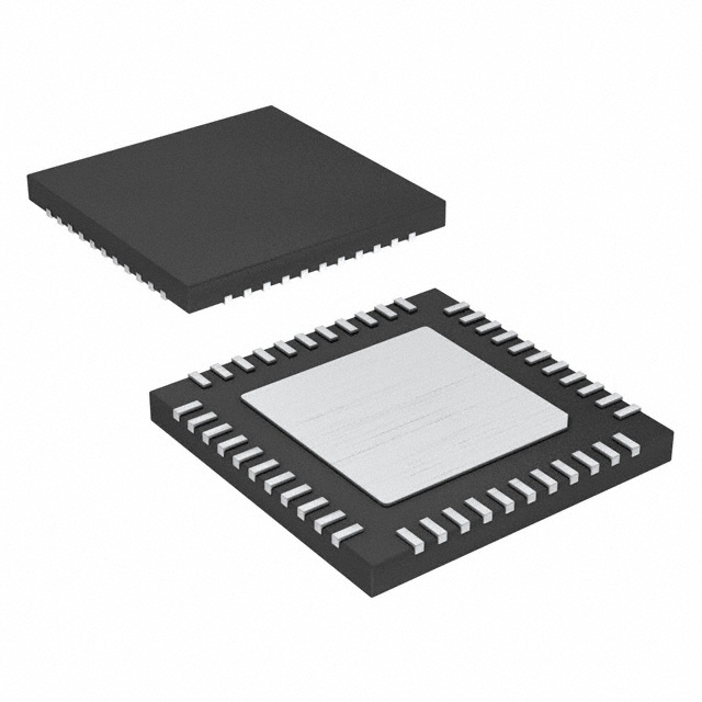
HVQFN44 plastic thermal enhanced very thin quad flat package; no leads; 44 terminals; SOT1113-1
body 9 9 0.85 mm
All information provided in this document is subject to legal disclaimers.
Rev. 1 — 13 July 2017
© NXP B.V. 2017. All rights reserved.
3 of 64
�TJA1086G
NXP Semiconductors
FlexRay active star coupler)
5. Block diagram
9,2
9%$7
9&&�
9&&�
9%8)�
9%8)�
�
��
��
��
��
��
7-$����*
,1+
,171
5671
��
�
��
67$7(
0$&+,1(
6&61
6&/.
6',
6'2
/:8
75;'�
75;'�
%*(
7;(1
7;'
5;'
:$.(�83
75$160,77(5
%86�(5525
5(&(,9(5
:$.(�83
75$160,77(5
%86�(5525
5(&(,9(5
��
%3B�
�
�
�
��
%0B�
63,
�
��
5287,1*
��
��
�
��
��
��
%3B�
%0B�
�
��
�
��
��
*1'�
*1'�
DDD�������
*1''
Fig 1.
Block diagram
TJA1086G
Product data sheet
All information provided in this document is subject to legal disclaimers.
Rev. 1 — 13 July 2017
© NXP B.V. 2017. All rights reserved.
4 of 64
�TJA1086G
NXP Semiconductors
FlexRay active star coupler)
6. Pinning information
�� 9&&�
�� 9%8)�
�� Q�F�
�� *1'�
�� 5(6�
�� 5(6�
�� 5(6�
�� 5(6�
�� 5(6�
�� 5(6�
�� 5671
6.1 Pinning
6&61
�
�� %3B�
6&/.
�
�� %0B�
6',
�
�� Q�F�
6'2
�
�� %3B�
,171
�
*1''
�
9,2
�
�� Q�F�
%*(
�
�� Q�F�
7;'
�
�� Q�F�
7;(1 ��
�� Q�F�
5;' ��
�� Q�F�
�� %0B�
9&&� ��
9%8)� ��
Q�F� ��
�� Q�F�
*1'� ��
Q�F� ��
9%$7 ��
/:8 ��
,1+ ��
Q�F� ��
75;'� ��
75;'� ��
7-$����*
DDD�������
7UDQVSDUHQW�WRS�YLHZ
Fig 2.
Pin configuration
6.2 Pin description
Table 3.
Pin description
Symbol Pin
TJA1086G
Product data sheet
Type[1]
Description
SCSN
1
I
SPI chip select input; internal pull-up
SCLK
2
I
SPI clock signal; internal pull-down
SDI
3
I
SPI data input; internal pull-down
SDO
4
O
SPI data output; 3-state output
INTN
5
O
interrupt output; open-drain output, low-side driver
GNDD
6
G
ground for digital circuits[2]
VIO
7
P
supply voltage for VIO voltage level adaptation
BGE
8
I
bus guardian enable input; internal pull-down
TXD
9
I
transmit data input; internal pull-down
TXEN
10
I
transmitter enable input; internal pull-up
RXD
11
O
receive data output
TRXD0
12
IO
data bus line 0 for inner star connection
TRXD1
13
IO
data bus line 1 for inner star connection
n.c.
14
-
not connected; to be connected to GND in application
INH
15
O
inhibit output; for switching external voltage regulator
All information provided in this document is subject to legal disclaimers.
Rev. 1 — 13 July 2017
© NXP B.V. 2017. All rights reserved.
5 of 64
�TJA1086G
NXP Semiconductors
FlexRay active star coupler)
Table 3.
TJA1086G
Product data sheet
Pin description …continued
Symbol Pin
Type[1]
Description
LWU
16
I
local wake-up input; internal pull-up or pull-down (depends on
voltage at pin LWU)
VBAT
17
P
battery supply voltage
n.c.
18
-
not connected; to be connected to GND in application
GND2
19
G
ground connection 2[2]
n.c.
20
-
not connected; to be connected to GND in application
VBUF2
21
P
buffer supply voltage 2[3]
VCC2
22
P
supply voltage 2[4]
n.c.
23
-
not connected; to be left open in the application
n.c.
24
-
not connected; to be left open in the application
n.c.
25
-
not connected; to be connected to GND in application
n.c.
26
-
not connected; to be left open in the application
n.c.
27
-
not connected; to be left open in the application
n.c.
28
-
not connected; to be connected to GND in application
BM_2
29
IO
bus line minus for branch 2[5]
BP_2
30
IO
bus line plus for branch 2[6]
n.c.
31
-
not connected; to be connected to GND in application
BM_1
32
IO
bus line minus for branch 1[5]
BP_1
33
IO
bus line plus for branch 1[6]
VCC1
34
P
supply voltage 1[4]
VBUF1
35
P
buffer supply voltage 1[3]
n.c.
36
-
not connected; to be connected to GND in application
GND1
37
G
ground connection 1[2]
RES6
38
-
reserved; to be connected to GND in application
RES5
39
-
reserved; to be connected to GND in application
RES4
40
-
reserved; to be connected to GND in application
RES3
41
-
reserved; to be connected to GND in application
RES2
42
-
reserved; to be connected to GND in application
RES1
43
-
reserved; to be connected to GND in application
RSTN
44
I
reset input; internal pull-up
[1]
IO: input/output; O: output; I: input; P: power supply; G: ground.
[2]
GND1, GND2, GNDD and the exposed center pad of HVQFN44 package must be connected together on
the PCB; references in the data sheet to GND can be assumed to encompass GND1, GND2, GNDD and
the exposed center pad of HVQFN4 unless stated otherwise.
[3]
VBUF1 and VBUF2 must be connected together on the PCB; note that references in the data sheet to VBUF
can be assumed to encompass VBUF1 and VBUF2 unless stated otherwise.
[4]
VCC1 and VCC2 must be connected together on the PCB; note that references in the data sheet to VCC can
be assumed to encompass VCC1 and VCC2 unless stated otherwise.
[5]
References in the data sheet to BM (e.g. pin BM or VBM) can be assumed to encompass BM_1 and BM_2
unless stated otherwise.
[6]
References in the data sheet to BP (e.g. pin BP or VBP) can be assumed to encompass BP_1 and BP_2
unless stated otherwise.
All information provided in this document is subject to legal disclaimers.
Rev. 1 — 13 July 2017
© NXP B.V. 2017. All rights reserved.
6 of 64
�TJA1086G
NXP Semiconductors
FlexRay active star coupler)
7. Functional description
7.1 Supply voltage
The TJA1086G state machine is adequately supplied if at least one of VBAT, VCC or VBUF
is available. The internal supply voltage to the state machine is denoted by VDIG. VBUF is
an auxiliary supply and is only needed for forwarding the wake-up pattern when VCC is not
available.
7.2 Host Control (HC) and Autonomous Power (AP) modes - APM flag
The APM flag determines whether the TJA1086G is host-controlled or is operating in
Autonomous Power mode. It is in AP mode by default.
The TJA1086G sets the APM flag:
•
•
•
•
at power-on
when a wake-up event is detected (on TXRD0/1, local or remote)
when a VCC undervoltage event is detected in AS_Normal mode
when a VIO undervoltage event lasts longer than tto(uvd)(VIO)
The host can set or reset the APM flag at any time.
7.3 Signal router
The signal router transfers data received on an input channel to all channels configured as
outputs. If data is being received on more than one input channel at the same time, the
channel that was first to signal activity is selected and data on the other channel/s is
ignored. Whether or not the data on an output channel is transmitted depends on whether
the output channel is enabled or disabled.
The TJA1086G contains the following data input channels:
• Branches 1 and 2
• TRXD0/1 interface (inner star interface)
• TXD/TXEN interface
The TJA1086G contains the following data output channels:
• Branches 1 and 2
• TRXD0/1 interface
• RXD pin
7.3.1 TRXD collision
When the TRXD0/1 interface is configured as an output channel, a TRXD collision is
detected (COLL_TRXD = 1) if pins TRXD0 and TRXD1 are both LOW for longer than
tdet(col)(TRXD), generating a CLAMP_ERROR interrupt.
When a TRXD collision is detected, the TJA1086G transmits a DATA_0 to all other active
output channels (irrespective of the actual data on the selected input channel), until the
selected input channel detects idle state.
TJA1086G
Product data sheet
All information provided in this document is subject to legal disclaimers.
Rev. 1 — 13 July 2017
© NXP B.V. 2017. All rights reserved.
7 of 64
�TJA1086G
NXP Semiconductors
FlexRay active star coupler)
7.4 Wake-up
The TJA1086G supports the following wake-up mechanisms:
• Remote wake-up via the bus (wake-up pattern or dedicated wake-up frame)
• Local wake-up via pin LWU
• Activity on the inner star interface (pins TRXD0 and TRXD1)
Any wake-up event will generate a WU interrupt. A remote wake-up on a branch will
generate an EVENT_BRx interrupt to indicate the branch where the wake-up pattern or
dedicated data frame was detected.
The host can identify the wake-up source by polling the General Status register
(WU_TRXD = 1 for a TRXD0/1 wake-up; WU_LOCAL = 1 for a local wake-up) and the
Branch Status register (WU_BRx = 1 for a remote wake-up).
7.4.1 Remote wake-up
When the TJA1086G is in AS_Standby or AS_Sleep, both branches are monitored for
wake-up events. When a valid wake-up pattern or data frame is detected on one of the
branches, the relevant WU_BRx status bit is set and the wake-up pattern/data frame is
forwarded to the other branch (if enabled).
A remote wake-up event occurring during an AS_Normal-to-AS_Standby or
AS_Normal-to-AS_Sleep transition will also be detected, setting the relevant WU_BRx
status bit and generating WU and EVENT_BRx interrupts.
7.4.1.1
Bus wake-up via wake-up pattern
A wake-up pattern consists of at least two consecutive wake-up symbols. A wake-up
symbol consists of a DATA_0 phase lasting longer than tdet(wake)DATA_0, followed by an idle
phase lasting longer than tdet(wake)idle, provided both wake-up symbols occur within a time
span of tdet(wake)tot (see Figure 3). The transceiver also wakes up if the idle phases are
replaced by DATA_1 phases.
A wake-up event is not detected if an invalid wake-up pattern is received. See Ref. 1 for
more details on invalid wake-up patterns.
TJA1086G
Product data sheet
All information provided in this document is subject to legal disclaimers.
Rev. 1 — 13 July 2017
© NXP B.V. 2017. All rights reserved.
8 of 64
�TJA1086G
NXP Semiconductors
FlexRay active star coupler)
ZDNH�XS
��WGHW�ZDNH�WRW
9GLI
�P9�
!�WGHW�ZDNH�LGOH
!�WGHW�ZDNH�LGOH
�
����
!�WGHW�ZDNH�'$7$B�
!�WGHW�ZDNH�'$7$B�
!�WGHW�ZDNH�LGOH
!�WGHW�ZDNH�LGOH
����
�
����
!�WGHW�ZDNH�'$7$B�
!�WGHW�ZDNH�'$7$B�
ZDNH�XS�V\PERO
ZDNH�XS�V\PERO
ZDNH�XS�SDWWHUQ
���DDD���
Fig 3.
Bus wake-up timing
See Ref. 1 for more details of the wake-up mechanism.
7.4.1.2
Bus wake-up via dedicated FlexRay data frame
The TJA1086G detects a wake-up event when a dedicated data frame emulating a valid
wake-up pattern, as shown in Figure 4, is received.
The Data_0 and Data_1 phases of the emulated wake-up symbol are interrupted by the
Byte Start Sequence (BSS) preceding each byte in the data frame. With a data rate of
10 Mbit/s, the interruption has a maximum duration of 130 ns and does not prevent the
transceiver from recognizing the wake-up pattern in the payload.
For longer interruptions at lower data rates (5 Mbit/s and 2.5 Mbit/s), the wake-up pattern
should be used (see Section 7.4.1.1).
TJA1086G
Product data sheet
All information provided in this document is subject to legal disclaimers.
Rev. 1 — 13 July 2017
© NXP B.V. 2017. All rights reserved.
9 of 64
�TJA1086G
NXP Semiconductors
FlexRay active star coupler)
9GLI
����QV
ZDNH�XS
����QV ����QV
�����
��9
�����
��� ��� ���
QV QV
QV
��� ���
QV
QV
��V
��V
��V
��V
���DDD���
The duration of each interruption is 130 ns.
The transition time from DATA_0 to DATA_1 and vice versa is about 20 ns.
The TJA1086G wake-up flag is set on receipt of the following frame payload:
0xFF, 0xFF, 0xFF, 0xFF, 0xFF, 0x00, 0x00, 0x00, 0x00, 0x00,
0xFF, 0xFF, 0xFF, 0xFF, 0xFF, 0x00, 0x00, 0x00, 0x00, 0x00,
0xFF, 0xFF, 0xFF, 0xFF, 0xFF, 0x00, 0x00, 0x00, 0x00, 0x00,
0xFF, 0xFF, 0xFF, 0xFF, 0xFF, 0xFF
Fig 4.
Minimum bus pattern for bus wake-up via dedicated FlexRay data frame
7.4.2 Local wake-up via pin LWU
Local wake-up is detected when the voltage on pin LWU is lower than Vth(wake)(LWU) for
longer than tdet(wake)(LWU) (falling edge on pin LWU). When local wake-up is detected, the
WU_LOCAL status bit is set and a WU interrupt is generated. At the same time, the
internal biasing of this pin is switched to pull-down.
If the voltage on pin LWU rises and remains above Vth(wake)(LWU) for longer than
tdet(wake)(LWU) (rising edge on pin LWU), local wake-up is not detected and the biasing on
pin LWU is switched to pull-up.
SXOO�XS
WGHW�ZDNH��/:8�
SXOO�XS
SXOO�GRZQ
WGHW�ZDNH��/:8�
9%$7
/:8
��9
WG�/:8ZDNH�,1++�
,1+
9%$7
��9
Fig 5.
���DDD���
Local wake-up timing on pin LWU
7.4.3 Wake-up via the TRXD0/1 interface
If the voltage on pin TRXD0 or pin TRXD1 is LOW for longer than tdet(wake)(TRXD), a WU
interrupt is generated and the WU_TRXD status bit is set.
TJA1086G
Product data sheet
All information provided in this document is subject to legal disclaimers.
Rev. 1 — 13 July 2017
© NXP B.V. 2017. All rights reserved.
10 of 64
�TJA1086G
NXP Semiconductors
FlexRay active star coupler)
7.5 Communication controller interface
7.5.1 Bus activity and idle detection
The following mechanisms for activity and idle detection are valid in normal power modes:
• If the absolute differential voltage on the bus lines is higher than Vi(dif)det(act) for
tdet(act)(bus), activity is detected on the bus lines
• If, after bus activity detection, the differential voltage on the bus lines is higher than
VIH(dif), pin RXD will go HIGH
• If, after bus activity detection, the differential voltage on the bus lines is lower than
VIL(dif), pin RXD will go LOW
• If the absolute differential voltage on the bus lines is lower than Vi(dif)det(act) for
tdet(idle)(bus), then idle is detected on the bus lines (pin RXD is switched HIGH or
remains HIGH)
Additionally, activity and idle can be detected:
• if pin TXEN is LOW for longer than tdet(act)(TXEN), activity is detected on pin TXEN
• if pin TXEN is HIGH for longer than tdet(idle)(TXEN), idle is detected on pin TXEN
• if pin TRXD0 or TRXD1 is LOW for longer than tdet(act)(TRXD), activity is detected on the
TRXD0/1 interface
• if pins TRXD0 and TRXD1 are both HIGH for longer than tdet(idle)(TRXD), idle is
detected on the TRXD0/1 interface
Transmitter input signals: TXD, TXEN and BGE[1]
Table 4.
TXD
TXEN
BGE
VIO UV
detected
RXD
Bus
TRXD0
X
H
X
no
HIGH
idle
high ohmic[2] high ohmic[2] AS_Normal
X
X
L
no
HIGH
idle
high ohmic[2] high ohmic[2] AS_Normal
L
L
H
no
LOW
DATA_0
LOW
H
L
H
no
HIGH
DATA_1
high ohmic[2] LOW
ohmic[2]
TRXD1
Operating mode
high ohmic[2] AS_Normal
high
ohmic[2]
AS_Normal
AS_Standby,[3] AS_Sleep[3]
X
X
X
no
HIGH
idle
high
X
X
X
yes
LOW
idle
high ohmic[2] high ohmic[2] AS_Normal,
AS_Standby,[3] AS_Sleep[3]
X
X
X
X
HIGH
float
high ohmic[2] high ohmic[2] AS_PowerOff, AS_Reset
[1]
The transmitter is activated by a falling edge on pin TXD while TXEN is LOW and BGE is HIGH.
[2]
Internal pull-up resistor (Rpu) to VBUF.
[3]
BP and BM biased to GND.
Table 5.
Bus
VIO UV
detected
RXD
TRXD0
TRXD1
Operating mode
DATA_0
no
LOW
LOW
high ohmic[1]
AS_Normal
DATA_1
no
HIGH
high ohmic[1]
LOW
AS_Normal
idle
no
HIGH
high ohmic[1]
high ohmic[1]
AS_Normal
HIGH
ohmic[1]
ohmic[1]
X
TJA1086G
Product data sheet
Bus as input
no
high
high
All information provided in this document is subject to legal disclaimers.
Rev. 1 — 13 July 2017
AS_Standby, AS_Sleep
© NXP B.V. 2017. All rights reserved.
11 of 64
�TJA1086G
NXP Semiconductors
FlexRay active star coupler)
Table 5.
Bus as input
Bus
VIO UV
detected
RXD
TRXD0
TRXD1
Operating mode
DATA_0
yes
LOW
LOW
high ohmic[1]
AS_Normal
LOW
AS_Normal
DATA_1
yes
LOW
high
ohmic[1]
ohmic[1]
high
ohmic[1]
idle
yes
LOW
high
X
yes
LOW
high ohmic[1]
high ohmic[1]
HIGH
ohmic[1]
ohmic[1]
X
[1]
X
high
high
AS_Normal
AS_Standby, AS_Sleep
AS_PowerOff, AS_Reset
Internal pull-up resistor (Rpu) to VBUF.
Table 6.
TRXD0/1 interface configured as input
TRXD0
TRXD1
X
RXD
Bus
Operating mode
falling edge no
HIGH
DATA_1
AS_Normal[1]
HIGH
HIGH
no
HIGH
idle
AS_Normal
falling edge
X
X
LOW
DATA_0
AS_Normal[1]
X
falling edge yes
LOW
DATA_1
AS_Normal[1]
HIGH
HIGH
yes
LOW
idle
AS_Normal
LOW
LOW
X
LOW
DATA_0
collision detected on TRXD0/1
[1]
VIO UV
detected
Activity detected on TRXD0/TRXD1.
7.6 Bus error detection
The TJA1086G provides bus error detection on each branch during data transmission.
When a transmit error (TxE_BRx = 1) is detected on a branch, an EVENT_BRx interrupt is
generated to notify the host.
The following conditions trigger bus error detection:
•
•
•
•
•
Short circuit BP to BM
Short-circuit BP to GND
Short-circuit BM to GND
Short-circuit BP to VCC or VBAT
Short-circuit BM to VCC or VBAT
7.7 Interrupt generation
Interrupts are generated when specific events take place or associated status bits in the
General or Branch X status registers are set. When an interrupt is generated, the relevant
interrupt status bit is set in the Interrupt Status register (see Table 10) and pin INTN is
forced LOW.
Some interrupt status bits (PWON, WU, SPI_ERROR and HC_ERROR) are reset
immediately after the Interrupt Status register has been read successfully (i.e. a rising
edge on SCSN with no SPI_ERROR).
TJA1086G
Product data sheet
All information provided in this document is subject to legal disclaimers.
Rev. 1 — 13 July 2017
© NXP B.V. 2017. All rights reserved.
12 of 64
�TJA1086G
NXP Semiconductors
FlexRay active star coupler)
The UV_ERROR, CLAMP_ERROR, TEMP_ERROR and EVENT_BRx status bits are
reset after the flag (or flags) that triggered the interrupt has been reset and a successful
read operation had been performed (these two events can occur in any order). Resetting
these bits triggers a further falling edge on INTN to indicate to the host that the issue that
triggered the interrupt has been resolved (except in the case of EVENT_BRx if a branch
wake-up event triggered the interrupt). See Section 7.10.2.3 for further details.
INTN signaling conforms to the FlexRay Electrical Physical Layer specification V3.0.1
(see Ref. 1).
7.8 Operating modes
The TJA1086G features five operating modes.
AS_PowerOff, AS_Sleep and AS_Standby are low-power modes in which the transceiver
is unable to transmit or receive data streams on the bus. In AS_PowerOff mode, only
power-on reset detection is active. The SPI, the low-power receiver and wake-up
detection are active in AS_Sleep mode. Undervoltage detection is enabled on VCC, VBAT
and VBUF in AS_Standby and AS_Normal modes. VIO undervoltage detection is always
enabled, except when the TJA1086G is in AS_PowerOff mode.
In AS_Normal mode, the TJA1086G can transmit and receive data streams on the bus.
Pin INH is HIGH in AS_Normal, AS_Standby and AS_Reset, and floating in AS_PowerOff
and AS_Sleep.
The dStarGoToSleep timer is started when the TJA1086G switches to AS_Standby or
AS_Normal, or when idle is detected on the bus. The timer is halted and reset when
activity is detected on the bus.
7.8.1 Operating mode transitions
7.8.1.1
AS_PowerOff
The TJA1086G switches to AS_PowerOff from any mode if the internal supply to the state
machine, VDIG, falls below the power-on detection threshold voltage (Vth(det)POR). It
remains in AS_PowerOff until VDIG rises above the power-on recovery threshold voltage
(Vth(rec)POR), when it switches to AS_Standby. Pins INTN and SDO are switched to a
high-impedance state in AS_PowerOff mode.
7.8.1.2
AS_Reset
The TJA1086G switches to AS_Reset from any mode if pin RSTN goes LOW with no
undervoltage detected on VIO. It remains in AS_Reset until pin RSTN goes HIGH, when it
switches to AS_Standby.
7.8.1.3
AS_Standby
The TJA1086G switches to AS_Standby:
- from AS_PowerOff when VDIG rises above the power-on recovery threshold voltage
(Vth(rec)POR)
- from AS_Reset when pin RSTN goes HIGH
- from AS_Normal when a VCC undervoltage event is detected (VCC < Vuvd(VCC) for
longer than tdet(uv)(VCC))
TJA1086G
Product data sheet
All information provided in this document is subject to legal disclaimers.
Rev. 1 — 13 July 2017
© NXP B.V. 2017. All rights reserved.
13 of 64
�TJA1086G
NXP Semiconductors
FlexRay active star coupler)
- from AS_Normal in response to a host ‘AS_Standby’ command (HC mode)
- from AS_Sleep in response to a host ‘AS_Standby’ command (HC mode)
- from AS_Sleep when a wake-up event is detected
The TJA1086G switches from AS_Standby:
- to AS_Normal when a wake-up event is detected, provided VBUF > Vuvr(VBUF)
- to AS_Normal when a VCC undervoltage recovery event is detected (VCC > Vuvr(VCC)
for longer than trec(uv)(VCC)), provided VBUF > Vuvr(BUF)
- to AS_Normal in response to a host ‘AS_Normal’ command (HC mode)
- to AS_Sleep if the dStarGoToSleep timer expires (AP mode)
- to AS_Sleep if a VCC undervoltage event lasts longer than tto(uvd)(VCC) (HC mode)
- to AS_Sleep in response to a host ‘AS_Sleep’ command (HC mode)
7.8.1.4
AS_Sleep
A wake-up event will trigger a transition to AS_Standby (followed by a transition to
AS_Normal if VBUF > Vuvr(VBUF)).
The TJA1086G switches to AS_Sleep:
- from AS_Standby in response to a host ‘AS_Sleep’ command (HC mode)
- from AS_Standby if the dStarGoToSleep timer expires (AP mode)
- from AS_Standby if a VCC undervoltage event lasts longer than tto(uvd)(VCC) (HC mode)
- from AS_Normal in response to a host ‘AS_Sleep’ command (HC mode)
- from AS_Normal if the dStarGoToSleep timer expires (AP mode)
The TJA1086G switches from AS_Sleep:
- to AS_Standby in response to a host ‘AS_Standby’ command (HC mode)
- to AS_Standby when a wake-up event is detected.
- to AS_Normal in response to a host ‘AS_Normal’ command (HC mode)
7.8.1.5
AS_Normal
The TJA1086G switches to AS_Normal:
- from AS_Standby if a VCC undervoltage recovery event is detected (VCC > Vuvr(VCC) for
longer than trec(uv)(VCC)), provided VBUF > Vuvr(BUF)
- from AS_Standby if a wake-up event is detected, provided VBUF > Vuvr(VBUF) for longer
than trec(uv)(VBUF)
- from AS_Standby or AS_Sleep in response to a host ‘AS_Normal’ command
The TJA1086G switches from AS_Normal:
- to AS_Standby when a VCC undervoltage event is detected (VCC < Vuvd(VCC) for longer
than tdet(uv)(VCC))
TJA1086G
Product data sheet
All information provided in this document is subject to legal disclaimers.
Rev. 1 — 13 July 2017
© NXP B.V. 2017. All rights reserved.
14 of 64
�TJA1086G
NXP Semiconductors
FlexRay active star coupler)
- if the TJA1086G is in HC mode, it will switch from AS_Standby to AS_Sleep if the
VCC undervoltage persists for longer than tto(uvd)(VCC)
- if the TJA1086G is in AP mode, it will switch to AS_Sleep when the
dStarGoToSleep timer expires
- to AS_Standby in response to a host ‘AS_Standby’ command (HC mode)
- to AS_Sleep in response to a host ‘AS_Sleep’ command (HC mode)
- to AS_Sleep if the dStarGoToSleep timer expires (AP mode)
TJA1086G
Product data sheet
All information provided in this document is subject to legal disclaimers.
Rev. 1 — 13 July 2017
© NXP B.V. 2017. All rights reserved.
15 of 64
�TJA1086G
NXP Semiconductors
FlexRay active star coupler)
7.8.1.6
Operating mode transition diagram
IURP�DQ\�PRGH
LI�9',*���9WK�GHW�325
$6B3RZHU2II
$6B5HVHW
IURP�DQ\�PRGH�LI
5671�JRHV�/2:�ZLWK
QR�9,2�XQGHUYROWDJH��
9',*�!�9WK�UHF�325
5671�JRHV�+,*+
$6B6WDQGE\
9&&�XQGHUYROWDJH�!
WWR�XYG��9&&��25
KRVW�FRPPDQG��
6OHHS
�
9&&�XQGHUYROWDJH�GHWHFWHG�25
KRVW�FRPPDQG��
6WDQGE\
�
�ZDNH�XS�HYHQW�$1'�9 %8)�!�9XYU�9%8)���25
�9&&�XQGHUYROWDJH�UHFRYHU\�
$1'�9%8)�!�9XYU�9%8)��
$6B1RUPDO
G6WDU*R7R6OHHS�WLPH�RXW
KRVW�FRPPDQG��
1RUPDO
�
ZDNH�XS�HYHQW�25
KRVW�FRPPDQG��
6WDQGE\
�
$6B6OHHS
KRVW�FRPPDQG��
6OHHS
�
G6WDU*R7R6OHHS�WLPH�RXW
+RVW�FRQWURO�PRGH�RQO\
$XWRQRPRXV�FRQWURO�PRGH�RQO\
Fig 6.
���DDD���
Mode transition diagram
TJA1086G
Product data sheet
All information provided in this document is subject to legal disclaimers.
Rev. 1 — 13 July 2017
© NXP B.V. 2017. All rights reserved.
16 of 64
�TJA1086G
NXP Semiconductors
FlexRay active star coupler)
7.9 Branch operating modes
Each of the two branches in the TJA1086G features six branch operating modes:
• Branch_Off
Both branches are in Branch_Off mode when the TJA1086G is in AS_PowerOff or
AS_Reset mode. The transmitter, normal receiver, low-power receiver and bus error
detection are disabled. The bus pins are floating.
• Branch_LowPower
Both branches are in Branch_LowPower mode when the TJA1086G is in AS_Standby
or AS_Sleep mode. The transmitter, the normal receiver and bus error detection are
disabled. The low-power receiver is active (i.e. remote wake-up is possible). The bus
pins are biased to ground.
• Branch_Disabled
The TJA1086G switches to Branch_Disabled if an overtemperature is detected. The
‘Branch_Disabled’ and ‘Branch_Normal’ commands allow the host to enable/disable a
branch without affecting the other branch. The transmitter, normal receiver and bus
error detection are disabled. Only the low-power receiver is active (remote wake-up is
possible). The bus pins are biased to Vo(idle)(BP) and Vo(idle)(BM).
• Branch_Normal
When a branch is in Branch_Normal, the TJA1086G will be in AS_Normal. The
transmitter, normal receiver and bus error detection are active. The bus pins are
biased to Vo(idle)(BP) and Vo(idle)(BM).
• Branch_TxOnly1
In Branch_TxOnly1 mode, the receiver is disabled, i.e. the received data is not
forwarded to the signal router. The transmitter is active and bus error detection is
active. The bus pins are biased to Vo(idle)(BP) and Vo(idle)(BM).
• Branch_TxOnly2
This mode is host-controlled only and is operationally identical to Branch_TxOnly1. It
allows the host to switch off the receiver in response to error conditions.
• Branch_FailSilent
The transmitter, the low-power receiver and bus error detection are disabled. Only the
receiver remains active to monitor the branch for idle or activity. Received data is not
forwarded to the signal router. The bus pins are biased to Vo(idle)(BP) and Vo(idle)(BM).
7.9.1 Branch operating mode transitions
Branch-related host commands can only be issued when the TJA1086G is in AS_Normal
mode.
7.9.1.1
Branch_Off
When the TJA1086G enters AS_PowerOff or AS_Reset, both branches switch to
Branch-Off. When the TJA1086G subsequently switches to AS_Standby, both branches
switch to Branch_LowPower.
7.9.1.2
Branch_LowPower
Both branches switch to Branch_LowPower when the TJA1086G enters AS_Standby or
AS_Sleep. Both branches will remain in this mode until the TJA1086G enters AS_Normal.
When this transition happens, any branch that was in Branch_Disabled before switching
to Branch_LowPower will return to Branch_Disabled. Otherwise, both branches switch to
TJA1086G
Product data sheet
All information provided in this document is subject to legal disclaimers.
Rev. 1 — 13 July 2017
© NXP B.V. 2017. All rights reserved.
17 of 64
�TJA1086G
NXP Semiconductors
FlexRay active star coupler)
Branch_Normal.
7.9.1.3
Branch_Disabled
An overtemperature event (TEMP_HIGH flag set) triggers a transition from
Branch_Normal to Branch_Disabled in both branches.
If an overtemperature event triggered the transition from Branch_Normal to
Branch_Disabled, both branches return to Branch_Normal when the overtemperature
problem has been resolved (TEMP_WARN flag reset).
The ‘Branch_Disabled’ and ‘Branch_Normal’ commands can be used to enable/disable
individual branches. A host command is also available to trigger a transition from
Branch_Disabled to Branch_TxOnly1 (‘Branch_TxOnly').
If a branch switches from Branch_Disabled to Branch_LowPower because the TJA1086G
has entered AS_Standby or AS_Sleep, it will return to Branch_Disabled when the
TJA1086G enters AS_Normal.
7.9.1.4
Branch_FailSilent
A branch switches to Branch_FailSilent:
- from Branch_Normal if a branch is clamped (Clamp_BRx flag set), provided
clamp-detection is enabled (bit CLAMP_DET set; see Table 9)
- from Branch_Normal if a transmit error (TxE_BRx = 1) is detected, provided
autonomous error confinement is enabled (bit AEC set; see Table 9)
- from Branch_TxOnly1 if a transmit error (TxE_BRx = 1) is detected.
The branch remains in Branch_FailSilent until idle is detected on both branches, when it
switches to Branch_TxOnly1 (a ‘Branch_TxOnly’ command is needed in HC mode).
7.9.1.5
Branch_TxOnly1
A branch switches to Branch_TxOnly1:
- from Branch_Disabled in response to a ‘Branch_TxOnly’ command (HC mode)
- from Branch_FailSilent in response to a ‘Branch_TxOnly’ command when both
branches are idle (HC mode)
- from Branch_FailSilent when both branches are idle (AP mode)
A branch switches from Branch_TxOnly1:
- to Branch_Normal when a transmission ends without error
- to Branch_FailSilent if a transmit error is detected (TxE_BRx = 1)
7.9.1.6
Branch_TxOnly2
This mode is purely host controlled. A branch switches to Branch_TxOnly2 only in
response to a ‘Branch_TxOnly’ command issued in Branch_Normal mode. The branch
remains in Branch_TxOnly2 mode until a ‘Branch_Normal’ command is received.
7.9.1.7
Branch_Normal
A branch switches to Branch_Normal:
TJA1086G
Product data sheet
All information provided in this document is subject to legal disclaimers.
Rev. 1 — 13 July 2017
© NXP B.V. 2017. All rights reserved.
18 of 64
�TJA1086G
NXP Semiconductors
FlexRay active star coupler)
- from Branch_LowPower when the TJA1086G enters AS_Normal mode (provided it
was not in Branch_Disabled before the transition to Branch_LowPower mode)
- from Branch_TxOnly2 in response to a host ‘Branch_Normal’ command
- from Branch_TxOnly1 when a transmission ends without error
- from Branch_Disabled in response to a host ‘Branch_Normal’ command
- from Branch_Disabled when an overtemperature is resolved (TEMP_WARN = 0),
provided the overtemperature triggered the earlier transition to Branch_Disabled.
A branch switches from Branch_Normal:
- to Branch_FailSilent if a branch is clamped, provided clamp-detection is enabled
(CLAMP_DET = 1)
- to Branch_FailSilent if a transmit error is detected, provided bit AEC = 1
- to Branch_TxOnly2 if a host ‘Branch_TxOnly’ command is received
- to Branch_Disabled if an overtemperature event is detected (TEMP_HIGH = 1)
TJA1086G
Product data sheet
All information provided in this document is subject to legal disclaimers.
Rev. 1 — 13 July 2017
© NXP B.V. 2017. All rights reserved.
19 of 64
�TJA1086G
NXP Semiconductors
FlexRay active star coupler)
7.9.1.8
Branch operating mode transition diagram
DFWLYH�VWDU�VZLWFKHV�WR
$6B6WDQGE\�RU�$6B6OHHS
%UDQFKB/RZ3RZHU
%UDQFKB2II
DFWLYH�VWDU�VZLWFKHV�WR
$6B1RUPDO
DFWLYH�VWDU�VZLWFKHV�WR
$6B3RZHU2II�RU�$6B5HVHW
$FWLYH�6WDU�&RXSOHU�LQ�
$6B1RUPDO�PRGH
SUHYLRXV�VWDWH�ZDV�
%UDQFKB'LVDEOHG
SUHYLRXV�VWDWH�QRW�
%UDQFKB'LVDEOHG
%UDQFKB'LVDEOHG
RYHUWHPSHUDWXUH�GHWHFWHG
%UDQFKB7[2QO\�
KRVW�FRPPDQG
�
%UDQFKB1RUPDO
�
RYHUWHPSHUDWXUH�ZDUQLQJ�LQDFWLYH
KRVW�FRPPDQG
�
%UDQFKB7[2QO\
�
KRVW�FRPPDQG
�
%UDQFKB'LVDEOHG
�
KRVW�FRPPDQG
�
%UDQFKB1RUPDO
�
%UDQFKB1RUPDO
FODPS�GHWHFWHG�25
WUDQVPLW�HUURU
ZLWK�$(&� ��
KRVW�FRPPDQG
�
%UDQFKB7[2QO\
�
%UDQFKB)DLO6LOHQW
WUDQVPLVVLRQ�HQGV
ZLWKRXW�HUURU
WUDQVPLW�HUURU
%UDQFKB7[2QO\�
DFWLYH�EUDQFKHV�LGOH�$1'
�$30�IODJ�VHW�25
KRVW�FRPPDQG
�
%UDQFKB7[2QO\
��
���DDD���
Fig 7.
Branch mode transition diagram
TJA1086G
Product data sheet
All information provided in this document is subject to legal disclaimers.
Rev. 1 — 13 July 2017
© NXP B.V. 2017. All rights reserved.
20 of 64
�TJA1086G
NXP Semiconductors
FlexRay active star coupler)
7.10 SPI interface
The TJA1086G contains a bidirectional 16-bit Serial Peripheral Interface (SPI) for
communicating with a host. The SPI allows the host to configure the TJA1086G and to
access error and status information.
7.10.1 Register access
The SPI supports full duplex data transfer, so status information is read out on pin SDO
while control data is being shifted in on pin SDI. Bit sampling is performed on the falling
edge of the clock signal on pin SCLK and data is shifted on the rising edge (MSB first; see
Figure 8).
The clock signal must be LOW when SCSN goes LOW to initiate an SPI register access
cycle.
6&61
6&/.
��
��
��
��
��
��
VDPSOHG
6',
6'2
;
IORDWLQJ
;
06%
��
��
��
��
/6%
06%
��
��
��
��
/6%
;
IORDWLQJ
���DDD���
Fig 8.
SPI register access
7.10.2 SPI registers
The SPI register structure in the TJA1086G is illustrated in Figure 9. The three MSBs
(bits15 to 13) contain the 3-bit register address. Bit 12 defines the selected register
access as read/write or read only. If bit 12 is 1, the SPI data transfer will be read only and
all data on the SDI pin will be ignored. If bit 12 is 0, data bits 11 to 0 will be written to the
selected register.
%LWV����WR�����UHJLVWHU�DGGUHVV
%LW������� ��5�2��UHDG�RQO\����� ��5�:��UHDG�ZULWH�
��
�
5HJLVWHU�6HOHFW
Fig 9.
TJA1086G
Product data sheet
'DWD�%LWV
���DDD���
SPI register structure
All information provided in this document is subject to legal disclaimers.
Rev. 1 — 13 July 2017
© NXP B.V. 2017. All rights reserved.
21 of 64
�TJA1086G
NXP Semiconductors
FlexRay active star coupler)
The assignment of control and status register addresses is detailed in Table 7. Data can
only be written to the Control and Configuration registers (status registers are read-only
by definition). Therefore the state of bit 12 is only evaluated when these registers are
being accessed.
Table 7.
Register map
Address bits 15, 14 and 13
Write access bit 12[1]
Register
000
0 =R/W, 1 = R/O
Control register; see Table 8
001
1 = R/O
Interrupt status register; see Table 10
010
1 = R/O
General status register; see Table 11
011
1 = R/O
Branch 1 status register; see Table 12
100
1 = R/O
Branch 2 status register; see Table 12
111
0 =R/W, 1 = R/O
Configuration register; see Table 9
[1]
Bit 12 is assumed to be 1 for status registers
The following subsections provide details of the bits in these registers and the control and
status functionality assigned to each.
TJA1086G
Product data sheet
All information provided in this document is subject to legal disclaimers.
Rev. 1 — 13 July 2017
© NXP B.V. 2017. All rights reserved.
22 of 64
�TJA1086G
NXP Semiconductors
FlexRay active star coupler)
7.10.2.1
Control register
The read/write Control register allows the host controller to set the operating modes and
to switch the TJA1086G between HC and AP modes.
Table 8.
Bit
Control register bit description
Symbol
11:10 OPM
Access
Default
Description
R/W
00
operating mode:
00: no change
01: AS_Standby
10: AS_Sleep
11: AS_Normal
9:8
CTRL_BR1
R/W
00
branch 1 control:
00: no change
01: Branch_Normal
10: Branch_TxOnly
11: Branch_Disabled
7:6
CTRL_BR2
R/W
00
branch 2 control:
00: no change
01: Branch_Normal
10: Branch_TxOnly
11: Branch_Disabled
5:2
reserved
1
APM[1]
after power-up, write 1111 once to bits [5:2] in
AS_Standby before entering AS_Normal to
minimize the power supply current
R/W
1
Autonomous Power mode
0: disabled
1: enabled
0
RESET_ERROR[2]
R/W
0
reset error flags and status bits
0: no change
1: reset flags/bits
TJA1086G
Product data sheet
[1]
The TJA1086G sets the APM flag at power-on, in response to a wake-up event (local, remote or TRXD), if
a VCC undervoltage is detected in AS_Normal or a VIO undervoltage is detected for longer than tto(uvd)(VIO).
[2]
Setting the RESET_ERROR bit resets all error status bits in the General Status (bits 8 to 1) and Branch
Status registers (bits 7 to 4).
All information provided in this document is subject to legal disclaimers.
Rev. 1 — 13 July 2017
© NXP B.V. 2017. All rights reserved.
23 of 64
�TJA1086G
NXP Semiconductors
FlexRay active star coupler)
7.10.2.2
Configuration register
The read/write Configuration register allows the host controller to configure a number of
TJA1086G parameters and functions.
Table 9.
Configuration register bit description
Bit
Symbol
Access
Default
Description
11
AEC
R/W
0
Autonomous error confinement:
0: disabled
1: enabled
10
BFT
R/W
1
Bus failure timer
0: disabled
1: enabled
9
WUD_BR1
R/W
1
wake-up detection on branch 1:
0: disabled
1: enabled
8
WUD_BR2
R/W
1
wake-up detection on branch 2:
0: disabled
1: enabled
7:6
reserved
5
CC_EN
after power-up, write 00 once to bits [7:6] to
minimize the power supply current
R/W
0
CC interface enable (TXD and TXEN inputs;
RXD output):
0: disabled
1: enabled
4
TRXD_EN
R/W
1
TRXD interface enable:
0: disabled
1: enabled
3
reserved
always 0
2
CLAMP_DET
R/W
1
clamping detection:
0: disabled
1: enabled
1
BIT_LATCHING
R/W
0
status bit latching:
0: disabled
1: enabled
0
TJA1086G
Product data sheet
PARITY
R
-
parity bit - odd parity (including parity bit)
All information provided in this document is subject to legal disclaimers.
Rev. 1 — 13 July 2017
© NXP B.V. 2017. All rights reserved.
24 of 64
�TJA1086G
NXP Semiconductors
FlexRay active star coupler)
Autonomous Error Confinement (AEC):
Setting the AEC bit enables the autonomous error confinement feature of the TJA1086G.
When AEC is enabled, a bus error (TxE_BRx = 1) triggers a transition from
Branch_Normal to Branch_FailSilent. AEC is disabled by default.
Bus Failure Timer (BFT):
Setting the BFT bit enables the bus failure timer.
When the BFT is enabled, pulses shorter than tto(BFT) are ignored, resulting in more robust
bus error detection. The BFT is enabled by default.
Wake-up detection on branch x (WUD_BRx):
Setting the WUD_BRx bit enables wake-up detection on the specified branch.
Each branch in a TJA1086G star network contains a low-power receiver for detecting
remote wake-up events. These events can be enabled and disabled individually. This
feature makes it possible to minimize quiescent current consumption, especially in
AS_Sleep mode. Wake-up detection is enabled by default on both branches.
Communication Controller interface Enable (CC_EN):
Setting bit CC_EN enables the communication controller interface.
A communication controller can be connected to the TJA1086G when CC_EN = 1. If
CC_EN = 0, the RXD output driver is switched off to minimize current consumption in
AS_Normal mode. The CC interface is disabled by default.
TRXD0/1 interface Enable (TRXD_EN):
Setting bit TRXD_EN enables the TRXD0 and TRXD1 interfaces.
When the TRXD0/1 interfaces are enabled, several TJA1086G devices can be connected
together to form a single active star. If only one TJA1086G is needed at any time, the
TRXD0/1 interfaces can be disabled to minimize current consumption in AS_Normal
mode. The TRXD0 and TRXD1 interfaces are enabled by default.
Clamp detection (CLAMP_DET):
Setting bit CLAMP_DET enables clamp detection on TXEN, TRXD and on both branches.
When clamp detection is enabled, a CLAMP_ERROR interrupt is generated if clamping is
detected on TXEN (CLAMP_TXEN = 1), TRXD (CLAMP_TRXD = 1) or on a branch
(CLAMP_BRx). Clamp detection is enabled by default.
Bit latching (BIT_LATCHING):
When bit latching is enabled (BIT_LATCHING = 1), the status bits in the General and
Branch X status registers reflect the latched state until the register is read. Once the
register has been read, latching is released and the bits then reflect the current ‘live’
status. When bit latching is disabled, the status bits reflect the ‘live’ status at all times. Bit
latching is disabled by default.
TJA1086G
Product data sheet
All information provided in this document is subject to legal disclaimers.
Rev. 1 — 13 July 2017
© NXP B.V. 2017. All rights reserved.
25 of 64
�TJA1086G
NXP Semiconductors
FlexRay active star coupler)
7.10.2.3
Interrupt Status register
The Interrupt Status register is read-only. When the TJA1086G sets a bit in this register, it
triggers a falling edge on pin INTN. Bits PWON, WU, SPI_ERROR and HC_ERROR are
reset after a successful read operation. The remaining bits are reset after the flag (or
flags) that triggered the interrupt has been reset and a successful read operation has
been performed (see Section 7.7).
Table 10.
Interrupt status register
Bit
Symbol
Description
11
PWON
power-on detection:
0: no power-on detected
1: power-on detected
10
WU
wake-up event detection (any):
0: no wake-up event detected
1: wake-up event detected
9
EVENT_BR1
wake-up or bus error detection on branch 1:
0: no wake-up or bus error detected
1: wake-up or bus error detected
8
EVENT_BR2
wake-up or bus error detection on branch 2:
0: no wake-up or bus error detected
1: wake-up or bus error detected
7:6
reserved
5
UV_ERROR
undervoltage detected on VBAT, VCC or VIO:
0: no undervoltage detected
1: undervoltage detected
4
CLAMP_ERROR
clamp error on TRXD, TXEN or branch or collision on TRXD:
0: no clamping error detected
1: clamping error detected
3
SPI_ERROR
SPI communication error:
0: not detected
1: detected
2
HC_ERROR
host command error:
0: not detected
1: detected
1
TEMP_ERROR
overtemperature error:
0: not detected
1:detected
0
TJA1086G
Product data sheet
PARITY
parity bit - odd parity (including parity bit)
All information provided in this document is subject to legal disclaimers.
Rev. 1 — 13 July 2017
© NXP B.V. 2017. All rights reserved.
26 of 64
�TJA1086G
NXP Semiconductors
FlexRay active star coupler)
PWON: A PWON interrupt is generated to signal a power-on event.
The PWON interrupt status bit is set when the TJA1086G leaves AS_PowerOff or
AS_Reset. It is reset after a successful read operation on the Interrupt Status register.
WU: A WU interrupt indicates the occurrence of a wake-up event.
The WU interrupt status bit is set when a wake-up event is detected on a branch
(WU_BRx = 1), on TRXD0/1 (WU_TRXD = 1), or on LWU (WU_LOCAL = 1). It is reset
after a successful read operation on the Interrupt Status register.
EVENT_BRx: An EVENT_BRx interrupt signals the occurrence of a significant event on
the relevant branch.
The EVENT_BRx interrupt status bit is set when any of the following events is detected on
a branch:
- a wake-up event (WU_BRx = 1)
- a bus error (TxE_BRx = 1)
- clamping (CLAMP_BRx = 1)
It is reset after the flag (or flags) that triggered the interrupt has been reset and the
Interrupt Status register has been read successfully. Resetting EVENT_BRx will trigger a
falling edge on INTN to indicate to the host that the event that triggered the interrupt has
been resolved (except when the interrupt was triggered by a branch wake-up event).
UV_ERROR: A UV_ERROR interrupt indicates that an undervoltage has occurred.
The UV_ERROR interrupt status bit is set when a VBAT (UV_VBAT = 1), VCC
(UV_VCC = 1) or VIO (UV_VIO = 1) undervoltage is detected. It is reset after the flag (or
flags) that triggered the interrupt has been reset and the Interrupt Status register has been
read successfully. Resetting UV_ERROR triggers a falling edge on INTN to indicate to the
host that the undervoltage condition is no longer present.
CLAMP_ERROR: A CLAMP_ERROR interrupt indicates that an input channel has
become clamped or a collision has occurred on the TRXDO/1 interface.
The CLAMP_ERROR interrupt status bit is set when clamping is detected on TRXD
(CLAMP_TRXD = 1), on TXEN (CLAMP_TXEN = 1) or on a branch (CLAMP_BRx = 1) or
if a collision is detected on TRXD0/TRXD1 (COLL_TRXD = 1). It is reset after the flag (or
flags) that triggered the interrupt has been reset and the Interrupt Status register has been
read successfully. Resetting CLAMP_ERROR triggers a falling edge on INTN to indicate
to the host that the clamp or collision error has been corrected.
SPI_ERROR: An SPI_ERROR interrupt indicates that an error has occurred during SPI
communications.
The SPI_ERROR interrupt status bit is set if the number of SCLK cycles generated during
a LOW phase on SCSN does not equal 16. It is reset after a successful read operation on
the Interrupt Status register.
HC_ERROR: A HC_ERROR interrupt indicates that an invalid host command has been
received.
TJA1086G
Product data sheet
All information provided in this document is subject to legal disclaimers.
Rev. 1 — 13 July 2017
© NXP B.V. 2017. All rights reserved.
27 of 64
�TJA1086G
NXP Semiconductors
FlexRay active star coupler)
The HC_ERROR interrupt status bit is set when the host requests an illegal mode
transition (as defined in the Section 7.8.1 and Section 7.9.1). It is reset after a successful
read operation on the Interrupt Status register.
TEMP_ERROR: A TEMP_ERROR interrupt signals the presence of an overtemperature
condition.
The TEMP_ERROR interrupt status bit is set when the temperature warning level
(TEMP_WARN = 1) or temperature high level (TEMP_HIGH = 1) is exceeded. It is reset
after the flag (or flags) that triggered the interrupt has been reset and the Interrupt Status
register has been read successfully. Resetting TEMP_ERROR triggers a falling edge on
INTN to indicate to the host that the overtemperature condition is no longer present.
TJA1086G
Product data sheet
All information provided in this document is subject to legal disclaimers.
Rev. 1 — 13 July 2017
© NXP B.V. 2017. All rights reserved.
28 of 64
�TJA1086G
NXP Semiconductors
FlexRay active star coupler)
7.10.2.4
General Status register
The read-only General Status register contains status information not included in the
Interrupt status register.
Table 11.
General status register
Bit
Symbol
Description
11
WU_LOCAL
local wake-up on pin LWU:
0: no wake-up detected
1: wake-up detected
10
WU_TRXD
wake-up via TRXD0/TRXD1
0: no wake-up detected
1: wake-up detected
9
BGE_FB
BGE status feedback:
0: if BGE is LOW
1: if BGE is HIGH
8
UV_VBAT
VBAT undervoltage
0: no undervoltage detected
1: undervoltage detected
7
UV_VCC
VCC undervoltage
0: no undervoltage detected
1: undervoltage detected
6
UV_VIO
VIO undervoltage
0: no undervoltage detected
1: undervoltage detected
5
TEMP_WARN
temperature warning level
0: not exceeded
1: exceeded
4
TEMP_HIGH
temperature high level
0: not exceeded
1: exceeded
3
CLAMP_TRXD
clamping detection on TRXD:
0: not detected
1: detected
2
CLAMP_TXEN
clamping detection on TXEN:
0: not detected
1: detected
1
COLL_TRXD
collision detection on TRXDO and TRXD1:
0: not detected
1:detected
0
TJA1086G
Product data sheet
PARITY
parity bit - odd parity (including parity bit)
All information provided in this document is subject to legal disclaimers.
Rev. 1 — 13 July 2017
© NXP B.V. 2017. All rights reserved.
29 of 64
�TJA1086G
NXP Semiconductors
FlexRay active star coupler)
WU_LOCAL:
WU_LOCAL is set when a local wake-up event is detected. A WU interrupt is generated.
WU_LOCAL is reset after the General Status register has been read successfully or when
the TJA1086G switches from AS_Normal to AS_Standby or AS_Sleep. This ensures that
a new wake-up event will be detected.
WU_TRXD:
WU_TRXD is set when a wake-up event is detected on the TRXD0/1 interface. A WU
interrupt is generated.
WU_TRXD is reset after the General Status register has been read successfully or when
the TJA1086G switches from AS_Normal to AS_Standby or AS_Sleep. This ensures that
a new wake-up event will be detected.
BGE_FB:
Bit BGE_FB provides information about the voltage level on pin BGE.
BGE_FB is set when the voltage on BGE is HIGH and reset when the voltage on BGE is
LOW.
UV_VBAT:
UV_VBAT is set when a VBAT undervoltage is detected, generating a UV_ERROR
interrupt.
If bit latching is enabled (BIT_LATCHING = 1), UV_BAT will remain set until the General
Status register has been read, after which it will reflect the current ‘live’ situation (set if
VBAT < Vuvd(VBAT) for longer than tdet(uv)(VBAT) and reset if VBAT > Vuvr(VBAT) for longer than
trec(uv)(VBAT)). If bit latching is not enabled, UV_BAT will reflect the ‘live’ situation at all
times.
UV_VCC:
UV_VCC is set when a VCC undervoltage is detected, generating a UV_ERROR interrupt.
If bit latching is enabled (BIT_LATCHING = 1), UV_VCC will remain set until the General
Status register has been read, after which it will reflect the current ‘live’ situation (set if
VCC < Vuvd(VCC) for longer than tto(uvd)(VCC) and reset if VCC > Vuvr(VCC) for longer than
tto(uvr)(VCC)). If bit latching is not enabled, UV_VCC will reflect the ‘live’ situation at all
times.
UV_VIO:
UV_VIO is set when a VIO undervoltage is detected, generating a UV_ERROR interrupt.
If bit latching is enabled (BIT_LATCHING = 1), UV_VIO will remain set until the General
Status register has been read, after which it will reflect the current ‘live’ situation (set if
VIO < Vuvd(VIO) for longer than tto(uvd)(VIO) and reset if VIO > Vuvr(VIO) for longer than
tto(uvr)(VIO)). If bit latching is not enabled, UV_VIO will reflect the ‘live’ situation at all times.
When a VIO undervoltage is active, the digital inputs are disabled and the TJA1086G is
unable to accept Host commands. If the VIO undervoltage persists for longer than
tto(uvd)(VIO), the APM flag is set and the TJA1086G switches from Host control to
Autonomous control.
TJA1086G
Product data sheet
All information provided in this document is subject to legal disclaimers.
Rev. 1 — 13 July 2017
© NXP B.V. 2017. All rights reserved.
30 of 64
�TJA1086G
NXP Semiconductors
FlexRay active star coupler)
TEMP_WARN:
TEMP_WARN is set when the junction temperature rises above the temperature warning
level, generating a TEMP_ERROR interrupt.
If bit latching is enabled (BIT_LATCHING = 1), TEMP_WARN will remain set until the
General Status register has been read, after which it will reflect the current ‘live’ situation
(set when Tj > Tj(warn) and reset when Tj < Tj(warn) with no activity on the bus or on the CC
and TRXD0/1 interfaces). If bit latching is not enabled, TEMP_WARN will reflect the ‘live’
situation at all times.
TEMP_HIGH:
TEMP_HIGH is set when the junction temperature rises above the temperature high level.
The output driver on the TRXD0/1 interface is disabled along with the branch transmitters
(both branches switch to Branch_Disabled). A TEMP_ERROR interrupt is generated.
If bit latching is enabled (BIT_LATCHING = 1), TEMP_HIGH will remain set until the
General Status register has been read, after which it will reflect the current ‘live’ situation
(set when Tj > Tj(high) and reset when Tj < Tj(high) with no activity on the bus or on the CC
and TRXD0/1 interfaces). If bit latching is not enabled, TEMP_HIGH will reflect the ‘live’
situation at all times.
CLAMP_TRXD:
CLAMP_TRXD is set when the TRXD0/1 interface is configured as an input and TRXD0
or TRXD1 is clamped LOW for longer than tdetCL(TRXD). The output driver on the TRXD0/1
interface is disabled and data on the inputs is ignored. A CLAMP_ERROR interrupt is
generated.
If bit latching is enabled, CLAMP_TRXD will remain set until the General Status register
has been read, after which it will reflect the current ‘live’ situation (set when TRXD0 or
TRXD1 clamped LOW and reset when TRXD0 and TRXD1 are HIGH). If bit latching is not
enabled, CLAMP_TRXD will reflect the ‘live’ situation at all times.
CLAMP_TXEN:
CLAMP_TXEN is set when the TXEN is clamped LOW for longer than tdetCL(TXEN). Data
on TXD/TXEN is ignored and a CLAMP_ERROR interrupt is generated.
If bit latching is enabled, CLAMP_TXEN will remain set until the General Status register
has been read, after which it will reflect the current ‘live’ situation (set when TXEN
clamped LOW and reset when TXEN is HIGH). If bit latching is not enabled,
CLAMP_TXEN will reflect the ‘live’ situation at all times.
COLL_TRXD:
COLL_TRXD is set when a collision is detected on the TRXD0/1 interface (TRXD0 and
TRXD1 LOW for longer than tdet(col)(TRXD)). A CLAMP_ERROR interrupt is generated.
COLL_TRXD is reset once the General Status register has been read.
TJA1086G
Product data sheet
All information provided in this document is subject to legal disclaimers.
Rev. 1 — 13 July 2017
© NXP B.V. 2017. All rights reserved.
31 of 64
�TJA1086G
NXP Semiconductors
FlexRay active star coupler)
7.10.2.5
Branch X status registers
There is a dedicated read-only status register for each branch, i.e. there are two Branch X
status registers in total. Each register contains relevant status information of a branch.
Table 12.
Branch X status register
Bit
Symbol
Description
11-9
STATE_BRx
state of active branch:
000: Branch_Normal mode
001: Branch_Disabled mode
010: Branch_LowPower mode
011: Branch_TxOnly_2 mode
100: Branch_FailSilent mode
101: Branch_TxOnly_1 mode
8
WU_BRx
wake-up status
0: no wake-up detected
1: wake-up detected
7
reserved
always 0
6
TxE_BRx
transmit error on branch
0: not detected
1: detected
5
reserved
always 0
4
CLAMP_BRx
clamp detection on branch
0: not detected
1: detected
TJA1086G
Product data sheet
3
reserved
always 0
2
reserved
always 1
1
reserved
always 0
0
PARITY
parity bit - odd parity (including parity bit)
All information provided in this document is subject to legal disclaimers.
Rev. 1 — 13 July 2017
© NXP B.V. 2017. All rights reserved.
32 of 64
�TJA1086G
NXP Semiconductors
FlexRay active star coupler)
STATE_BRx:
Bits STATE_BRx indicate the current branch operating mode.
WU_BRx:
WU_BRx is set when a remote wake-up event is detected on a branch. A WU interrupt is
generated along with an EVENT_BRx interrupt to indicate the branch where the wake-up
pattern or dedicated data frame was detected.
WU_BRx is reset after the Branch Status register has been read successfully or when the
TJA1086G switches from AS_Normal to AS_Standby or AS_Sleep. This ensures that a
new wake-up event will be detected.
TxE_BRx:
TxE_BRx is set when a transmit error is detected on a branch, generating an
EVENT_BRx interrupt. A transmit error is detected when there is a mismatch between the
transmitted and received signals.
If bit latching is enabled (BIT_LATCHING = 1), TxE_BRx will remain set until the register
has been read, after which it is reset if no mismatch is found between transmitted and
received signals or the branch leaves Branch_Normal. If bit latching is not enabled,
TxE_BRx is reset if no mismatch is found in a data frame or the branch leaves
Branch_Normal.
CLAMP_BRx:
CLAMP_BRx is set when a branch is clamped for longer than tdetCL(bus), generating a
CLAMP_ERROR interrupt along with an EVENT_BRx interrupt to indicate the branch.
If bit latching is enabled (BIT_LATCHING = 1), CLAMP_BRx will remain set until the
register has been read, after which it is reset when idle is detected on the branch. If bit
latching is not enabled, CLAMP_BRx is reset when idle is detected on the branch.
TJA1086G
Product data sheet
All information provided in this document is subject to legal disclaimers.
Rev. 1 — 13 July 2017
© NXP B.V. 2017. All rights reserved.
33 of 64
�TJA1086G
NXP Semiconductors
FlexRay active star coupler)
8. Limiting values
Table 13. Limiting values
In accordance with the Absolute Maximum Rating System (IEC 60134). All voltages are referenced to GND.
Symbol
Parameter
Conditions
VBAT
battery supply voltage
IINH
current on pin INH
voltage on pin
Vx
IO(LWU)
x[1]
Tamb
ambient temperature
Tvj
virtual junction temperature
Tstg
storage temperature
VESD
Max
Unit
0.3
+48
V
during load dump (400 ms max.)
0.3
+60
V
AS_Normal, AS_Standby or AS_Reset
1
0
mA
on pins VCC, VBUF, VIO, TRXD0, TRXD1,
BGE, TXD, TXEN, RSTN, INTN, SCSN,
SCLK, SDI, SDO
0.3
+5.5
V
on pins INH, LWU
0.3
VBAT + 0.3
V
on pin RXD
0.3
min(VIO +
0.3, 5.5)
V
on any BM/BP pin with respect to other
BP/BM pins and GND
60
+60
V
15
-
mA
output current on pin LWU
transient voltage
Vtrt
Min
[1]
on pins LWU, VBAT, BP and BM
[2]
pulse 1
100
-
V
pulse 2a
-
75
V
pulse 3a
150
-
V
pulse 3b
-
100
V
40
+125
C
40
+150
C
55
+150
C
[3]
electrostatic discharge voltage
IEC 61000-4-2 (150 pF, 330 )
[4]
6.0
+6.0
kV
on pin LWU to GND
[5]
6.0
+6.0
kV
on pin VBAT to GND
[6]
6.0
+6.0
kV
8.0
+8.0
kV
6.0
+6.0
kV
4.0
+4.0
kV
200
+200
V
1000
+1000
V
on pins BP and BM to GND
Human Body Model (HBM); 100 pF,
1.5 k
[7]
on pins BP and BM to GND
on pins LWU and VBAT to GND
[8]
on any other pin
Machine Model (MM); 200 pF, 0.75 H,
10
[9]
on any pin
Charged Device Model (CDM); field
Induced charge; 4 pF
on any pin
[10]
[1]
The device can sustain voltages up to the specified values over the product lifetime, provided applied voltages (including transients)
never exceed these values.
[2]
According to IEC TS 62228 (2007), Section 4.2.4; parameters for standard pulses defined in ISO7637 part 2: 2004-06.
[3]
In accordance with IEC 60747-1. An alternative definition of Tvj is: Tvj = Tamb + P Rth(j-a), where Rth(j-a) is a fixed value used in the
calculation of Tvj. The rating for Tvj limits the allowable combinations of power dissipation (P) and ambient temperature (Tamb).
TJA1086G
Product data sheet
All information provided in this document is subject to legal disclaimers.
Rev. 1 — 13 July 2017
© NXP B.V. 2017. All rights reserved.
34 of 64
�TJA1086G
NXP Semiconductors
FlexRay active star coupler)
[4]
According to IEC TS 62228 (2007), Section 4.3; DIN EN 61000-4-2; verified by an external test house. The test result is equal to or
better than 6 kV (unaided).
[5]
With 3.3 k in series and 10 nF capacitor from LWU to GND.
[6]
With 100 nF from VBAT to GND.
[7]
According to AEC-Q100-002.
[8]
Guaranteed only when all n.c. pins are connected to GND.
[9]
According to AEC-Q100-003.
[10] According to AEC-Q100-011 Rev-C1. The classification level is C6.
9. Thermal characteristics
Table 14.
Symbol
Rth(j-a)
Rth(j-c)
Thermal characteristics
Parameter
Conditions
thermal resistance from junction to ambient
thermal resistance from junction to case
Typ
Unit
dual-layer board
[1]
44
K/W
four-layer board
[2]
22
K/W
3
K/W
in free air
[1]
According to JEDEC JESD51-2, JESD51-3 and JESD51-5 at natural convection on 1s board with thermal via array under the exposed
pad connected to the second copper layer.
[2]
According to JEDEC JESD51-2, JESD51-5 and JESD51-7 at natural convection on 2s2p board. Board with two inner copper layers
(thickness: 35 m) and thermal via array under the exposed pad connected to the first inner copper layer.
TJA1086G
Product data sheet
All information provided in this document is subject to legal disclaimers.
Rev. 1 — 13 July 2017
© NXP B.V. 2017. All rights reserved.
35 of 64
�TJA1086G
NXP Semiconductors
FlexRay active star coupler)
10. Static characteristics
Table 15. Static characteristics
All parameters are guaranteed for VBAT = 4.45 V to 60 V; VCC = 4.45 V to 5.25 V; VBUF = 4.45 V to 5.25 V;VIO = 2.55 V to
5.25 V; Tvj = 40 C to +150 C; Cbus = 100 pF; Rbus = 40 to 55 ; CRXD = 15 pF and CTRXD0 = CTRXD1 = 50 pF unless
otherwise specified. All voltages are defined with respect to ground; positive currents flow into the IC.
Symbol
Parameter
Conditions
Min
Typ
Max
Unit
Supply: pin VBAT
VBAT
battery supply voltage
operating range
4.75
-
60
V
IBAT
battery supply current
AS_Normal; no load on INH
-
0.1
1
mA
AS_Standby; no load on INH;
wake-up enabled on both
branches; bits [7:6] in
Configuration register (Table 9) set
to 11
-
50
100
A
AS_Standby; no load on INH;
wake-up enabled on both
branches; bits [7:6] in
Configuration register set to 00
-
38
80
A
AS_Sleep; wake-up enabled on
both branches; bits [7:6] in
Configuration register set to 11
-
50
100
A
AS_Sleep; wake-up enabled on
both branches; bits [7:6] in
Configuration register set to 00
-
38
80
A
AS_Sleep; wake-up enabled on
both branches; bits [7:6] in
Configuration register set to 11;
Tvj 85 C
-
50
90
A
AS_Sleep; wake-up enabled on
both branches; bits [7:6] in
Configuration register set to 00;
Tvj 85 C
-
38
70
A
AS_Sleep; wake-up disabled on
both branches
-
25
55
A
AS_Sleep; wake-up disabled on
both branches; Tvj 85 C
-
25
45
A
Vuvd
undervoltage detection
voltage
4.45
-
4.715
V
Vuvr
undervoltage recovery
voltage
4.475
-
4.74
V
Vuvhys
undervoltage hysteresis
voltage
25
-
290
mV
Power-on reset for VDIG
Vth(det)POR
power-on reset detection
threshold voltage
of internal digital circuitry
3
-
3.4
V
Vth(rec)POR
power-on reset recovery
threshold voltage
of internal digital circuitry
3.1
-
3.5
V
Vhys(POR)
power-on reset hysteresis
voltage
of internal digital circuitry
100
500
mV
TJA1086G
Product data sheet
All information provided in this document is subject to legal disclaimers.
Rev. 1 — 13 July 2017
© NXP B.V. 2017. All rights reserved.
36 of 64
�TJA1086G
NXP Semiconductors
FlexRay active star coupler)
Table 15. Static characteristics …continued
All parameters are guaranteed for VBAT = 4.45 V to 60 V; VCC = 4.45 V to 5.25 V; VBUF = 4.45 V to 5.25 V;VIO = 2.55 V to
5.25 V; Tvj = 40 C to +150 C; Cbus = 100 pF; Rbus = 40 to 55 ; CRXD = 15 pF and CTRXD0 = CTRXD1 = 50 pF unless
otherwise specified. All voltages are defined with respect to ground; positive currents flow into the IC.
Symbol
Parameter
Conditions
Min
Typ
Max
Unit
V(VCC-VDIG)
voltage difference between
VCC and VDIG
VCC = 4.45 V; VBAT = VBUF = 0 V
-
-
1.0
V
V(VBAT-VDIG)
voltage difference between
VBAT and VDIG
VBAT = 4.45 V; VCC = VBUF = 0 V
-
-
1.0
V
V(VBUF-VDIG)
voltage difference between
VBUF and VDIG
VBUF = 4.45 V; VCC = VBAT = 0 V
-
-
1.0
V
Supply: pins VCC1 and VCC2 (connected on the PCB)
VCC
ICC
supply voltage
operating range
supply current
4.75
-
5.25
V
AS_Normal; VTXEN = 0 V;
VBGE = VIO; Rbus = 45 ;
both branches in Branch_Normal;
bits [5:2] in Control register
(Table 8) set to 0000
[1]
-
95
120
mA
AS_Normal; VTXEN = 0 V;
VBGE = VIO; Rbus = 45 ;
both branches in Branch_Normal;
bits [5:2] in Control register set
to 1111
[1]
-
95
120
mA
AS_Normal; VTXEN = VIO;
VBGE = 0 V; Rbus = 45 ;
both branches in Branch_Normal
and/or Branch_Disabled
[1]
-
-
80
mA
AS_Standby
[1][2]
-
4
35
A
AS_Standby; Tvj 85 C
[1][2]
-
4
15
A
AS_Sleep, AS_Reset
[1][2]
-
0
30
A
AS_Sleep, AS_Reset; Tvj 85 C
[1][2]
-
0
10
A
Vuvd
undervoltage detection
voltage
4.45
-
4.715
V
Vuvr
undervoltage recovery
voltage
4.475
-
4.74
V
Vuvhys
undervoltage hysteresis
voltage
25
-
290
mV
5.5 V VBAT 60 V;
VCC Vuvd(VCC)
4.5
-
5.25
V
4.5 V VBAT 5.5 V;
VCC Vuvd(VCC)
3.5
-
5.25
V
Supply: pins VBUF1 and VBUF2 (connected on the PCB)
VBUF
supply voltage on pin VBUF
V(VCC-VBUF)
voltage difference between
VCC and VBUF
VCC Vuvr(VCC)
0
-
0.25
V
Ich(VBAT-VBUF)
charge current from VBAT to
VBUF
5.5 V VBAT 60 V;
VCC Vuvd(VCC); 0 V VBUF 4 V
200
100
30
A
Vuvd
undervoltage detection
voltage
4.2
-
4.474
V
Vuvr
undervoltage recovery
voltage
4.225
-
4.499
V
TJA1086G
Product data sheet
All information provided in this document is subject to legal disclaimers.
Rev. 1 — 13 July 2017
© NXP B.V. 2017. All rights reserved.
37 of 64
�TJA1086G
NXP Semiconductors
FlexRay active star coupler)
Table 15. Static characteristics …continued
All parameters are guaranteed for VBAT = 4.45 V to 60 V; VCC = 4.45 V to 5.25 V; VBUF = 4.45 V to 5.25 V;VIO = 2.55 V to
5.25 V; Tvj = 40 C to +150 C; Cbus = 100 pF; Rbus = 40 to 55 ; CRXD = 15 pF and CTRXD0 = CTRXD1 = 50 pF unless
otherwise specified. All voltages are defined with respect to ground; positive currents flow into the IC.
Symbol
Parameter
Vuvhys
undervoltage hysteresis
voltage
Conditions
Min
Typ
Max
Unit
25
-
299
mV
2.8
-
5.25
V
Supply: pin VIO
VIO
supply voltage on pin VIO
operating range
IIO
supply current on pin VIO
AS_Normal; VTXD = VIO
-
-
1
mA
AS_Standby; AS_Sleep;
AS_PowerOff;
VSCSN = VTXEN = VRSTN = VVIO
-
2
7
A
from digital input pin to VIO;
AS_PowerOff;
VTXEN = VTXD = VBGE = VSCSN =
VSCLK = VSDI = VRSTN = 5.25 V;
VCC = VIO = 0 V
5
-
+5
A
Ir
reverse current
Vuvd
undervoltage detection
voltage
2.55
-
2.765
V
Vuvr
undervoltage recovery
voltage
2.575
-
2.79
V
Vuvhys
undervoltage hysteresis
voltage
25
-
240
mV
Pin TXEN
VIH
HIGH-level input voltage
AS_Normal
0.7VIO
-
5.5
V
VIL
LOW-level input voltage
AS_Normal
0.3
-
0.3VIO
V
IIH
HIGH-level input current
VTXEN = VIO
2
-
+2
A
IIL
LOW-level input current
VTXEN = 0.3VIO
300
-
50
A
VIH
HIGH-level input voltage
AS_Normal
0.6VIO
-
5.5
V
VIL
LOW-level input voltage
AS_Normal
0.3
-
0.4VIO
V
Rpd
pull-down resistance
to GND
50
150
400
k
-
-
10
pF
0.7VIO
-
5.5
V
Pin TXD
[3]
input capacitance
with respect to all other pins at
ground; VTXD = 100 mV; f = 5 MHz
VIH
HIGH-level input voltage
AS_Normal
VIL
LOW-level input voltage
AS_Normal
0.3
-
0.3VIO
V
Rpd
pull-down resistance
to GND
50
150
400
k
IOH
HIGH-level output current
VRXD = VIO 0.4 V
15
-
1
mA
IOL
LOW-level output current
VRXD = 0.4 V
1
-
15
mA
VOH
HIGH-level output voltage
IOH(RXD) = 1 mA
VIO
0.4
-
VIO
V
VOL
LOW-level output voltage
IOL(RXD) = 1 mA
-
-
0.4
V
Ci
Pin BGE
Pin RXD
TJA1086G
Product data sheet
All information provided in this document is subject to legal disclaimers.
Rev. 1 — 13 July 2017
© NXP B.V. 2017. All rights reserved.
38 of 64
�TJA1086G
NXP Semiconductors
FlexRay active star coupler)
Table 15. Static characteristics …continued
All parameters are guaranteed for VBAT = 4.45 V to 60 V; VCC = 4.45 V to 5.25 V; VBUF = 4.45 V to 5.25 V;VIO = 2.55 V to
5.25 V; Tvj = 40 C to +150 C; Cbus = 100 pF; Rbus = 40 to 55 ; CRXD = 15 pF and CTRXD0 = CTRXD1 = 50 pF unless
otherwise specified. All voltages are defined with respect to ground; positive currents flow into the IC.
Symbol
Parameter
Conditions
Min
Typ
Max
Unit
VO
output voltage
when undervoltage on VIO;
VCC 4.75 V; RL = 100 k to GND
-
-
500
mV
VCC = VBAT = VBUF = 0 V;
RL = 100 k to VIO
VIO
500
-
VIO
mV
Pin RSTN
VIH
HIGH-level input voltage
0.7VIO
-
5.5
V
VIL
LOW-level input voltage
0.3
-
0.3VIO
V
IIH
HIGH-level input current
VRSTN = VIO
1
-
+1
A
IIL
LOW-level input current
VRSTN = 0.3VIO
300
-
30
A
V
Pins TRXD0 and TRXD1
VIH
HIGH-level input voltage
0.7VBUF -
5.5
VIL
LOW-level input voltage
0.3
0.3VBUF V
VOL
LOW-level output voltage
Rpu = 200
Ci
input capacitance
with respect to all other pins at
GND; VTXD = 100 mV; f = 5 MHz
Rpu
pull-up resistance
to VBUF
VIH(dif)
differential HIGH-level input
voltage
AS_Normal; 10 V Vcm +15 V
VIL(dif)
differential LOW-level input
voltage
AS_Normal; 10 V Vcm +15 V
Vi(dif)(H-L)
differential input voltage
difference between
HIGH-level and LOW-level
Vcm = 2.5 V; AS_Normal
VOH(dif)
differential HIGH-level
output voltage
-
0.3
-
+0.8
V
-
-
15
pF
2.5
5
10
k
[4]
150
-
300
mV
[4]
300
-
150
mV
400
-
125
mV
30
-
+30
mV
4.75 V VBUF 5.25 V
600
-
2000
mV
4.45 V VBUF 5.25 V
530
-
2000
mV
600
mV
530
mV
[3]
Pins BP and BM
AS_Standby; AS_Sleep;
10 V Vcm +15 V
[4]
[4]
VOL(dif)
differential LOW-level output 4.75 V VBUF 5.25 V
voltage
4.45 V VBUF 5.25 V
2000
-
2000
-
Vo(idle)(BP)
idle output voltage on pin BP Branch_Normal
0.4VBUF -
0.6VBUF V
Branch_LowPower
0.1
+0.1
Branch_Normal
0.4VBUF -
-
V
Vo(idle)(BM)
idle output voltage on pin
BM
0.1
-
+0.1
V
Io(idle)BP
idle output current on pin BP 60 V VBP +60 V; no bus load
7.5
-
+7.5
mA
Io(idle)BM
idle output current on pin BM 60 V VBM +60 V; no bus load
7.5
-
+7.5
mA
Vo(idle)(dif)
differential idle output
voltage
25
0
+25
mV
Vi(dif)det(act)
activity detection differential
input voltage (absolute
value)
150
-
300
mV
Vcm(bus)(DATA_0)
DATA_0 bus common-mode Branch_Transmit
voltage
0.65
VBUF
V
TJA1086G
Product data sheet
Branch_LowPower
AS_Normal; 10 V Vcm +15 V
All information provided in this document is subject to legal disclaimers.
Rev. 1 — 13 July 2017
[4]
0.4VBUF -
0.6VBUF V
© NXP B.V. 2017. All rights reserved.
39 of 64
�TJA1086G
NXP Semiconductors
FlexRay active star coupler)
Table 15. Static characteristics …continued
All parameters are guaranteed for VBAT = 4.45 V to 60 V; VCC = 4.45 V to 5.25 V; VBUF = 4.45 V to 5.25 V;VIO = 2.55 V to
5.25 V; Tvj = 40 C to +150 C; Cbus = 100 pF; Rbus = 40 to 55 ; CRXD = 15 pF and CTRXD0 = CTRXD1 = 50 pF unless
otherwise specified. All voltages are defined with respect to ground; positive currents flow into the IC.
Symbol
Parameter
Conditions
Vcm(bus)(DATA_1)
DATA_1 bus common-mode Branch_Transmit
voltage
Ri
input resistance
Ri(dif)(BP-BM)
differential input resistance
between pin BP and pin BM
Zo(eq)TX
transmitter equivalent output Cbus = 100 pF; Rbus = 40 or
impedance
100
Ci(BP)
Max
Unit
0.4VBUF -
0.65
VBUF
V
Rbus =
10
20
40
k
Rbus =
20
40
80
k
[5]
35
-
100
input capacitance on pin BP with respect to all other pins at
GND; VBP = 100 mV; f = 5 MHz
[3]
-
-
15
pF
Ci(BM)
input capacitance on pin BM with respect to all other pins at
GND; VBM = 100 mV; f = 5 MHz
[3]
-
-
15
pF
Ci(dif)(BP-BM)
differential input capacitance VBP = 100 mV; VBM = 100 mV;
between pin BP and pin BM f = 5 MHz
[3]
-
-
5
pF
ILI(BP)
input leakage current on pin
BP
5
0
+5
A
1600
-
+1600
A
5
0
+5
A
AS_PowerOff; VBP = VBM;
0 V VBP 5 V
loss of ground; VBP = VBM = 0 V;
all other pins connected to 16 V via
0
ILI(BM)
IO(sc)
input leakage current on pin
BM
short-circuit output current
(absolute value)
Min
[3]
AS_PowerOff; VBP = VBM;
0 V VBM 5 V
Typ
loss of ground; VBP = VBM = 0 V;
all other pins connected to 16 V via
0
[3]
1600
-
+1600
A
on pin BP; 5 V VBP +60 V;
Rsc 1 ; tsc 1500 s
[6][8]
-
-
60
mA
on pin BM; 5 V VBM +60 V;
Rsc 1 ; tsc 1500 s
[6][8]
-
-
60
mA
on pins BP and BM; VBP = VBM;
Rsc 1 ; tsc 1500 s
[7][8]
-
-
60
mA
IINH = 0.2 mA: AS_Normal;
AS_Standby; AS_Reset
VBAT
0.8
-
VBAT
V
Pin INH
VOH
HIGH-level output voltage
IL
leakage current
AS_Sleep; AS_PowerOff
3
-
+3
A
IO(sc)
short-circuit output current
VINH = 0 V; AS_Normal;
AS_Standby; AS_Reset
7
-
1
mA
Vth(wake)LWU
wake-up threshold voltage
on pin LWU
AS_Sleep; AS_Standby
2
-
3.75
V
Vhys(wake)LWU
wake-up hysteresis voltage
on pin LWU
0.3
-
1.2
V
IIL
LOW-level input current
Pin LWU
TJA1086G
Product data sheet
VLWU = 2 V for t > tdet(wake)(LWU)
3
-
11
A
VLWU = 0 V
2
-
0.3
A
All information provided in this document is subject to legal disclaimers.
Rev. 1 — 13 July 2017
© NXP B.V. 2017. All rights reserved.
40 of 64
�TJA1086G
NXP Semiconductors
FlexRay active star coupler)
Table 15. Static characteristics …continued
All parameters are guaranteed for VBAT = 4.45 V to 60 V; VCC = 4.45 V to 5.25 V; VBUF = 4.45 V to 5.25 V;VIO = 2.55 V to
5.25 V; Tvj = 40 C to +150 C; Cbus = 100 pF; Rbus = 40 to 55 ; CRXD = 15 pF and CTRXD0 = CTRXD1 = 50 pF unless
otherwise specified. All voltages are defined with respect to ground; positive currents flow into the IC.
Symbol
Parameter
Conditions
Min
Typ
Max
Unit
IIH
HIGH-level input current
VLWU = 3.75 V for t > tdet(wake)(LWU);
4.75 V VBAT +60 V
11
-
3
A
VLWU = VBAT
0.2
-
1.2
A
Pin SDO
VOH
HIGH-level output voltage
IOH(SDO) = 0.5 mA
VIO
0.4
-
VIO
V
VOL
LOW-level output voltage
IOL(SDO) = 0.5 mA
-
-
0.4
V
IOH
HIGH-level output current
VSDO = VIO 0.4 V
8
2
0.5
mA
IOL
LOW-level output current
VSDO = 0.4 V
0.5
2
8
mA
IL
leakage current
SCSN HIGH
5
-
+5
A
VO
output voltage
when undervoltage on VIO;
VCC 4.75 V; RL = 100 k to GND
-
-
500
mV
VCC = VBAT = VBUF = 0 V;
RL = 100 k to GND
-
-
500
mV
0.7VIO
-
5.5
V
Pin SDI
VIH
HIGH-level input voltage
VIL
LOW-level input voltage
Rpd
pull-down resistance
to GND
0.3
-
0.3VIO
V
50
150
400
k
0.7VIO
-
5.5
V
Pin SCSN
VIH
HIGH-level input voltage
VIL
LOW-level input voltage
0.3
-
0.3VIO
V
IIH
HIGH-level input current
VSCSN = VIO
1
-
+1
A
IIL
LOW-level input current
VSCSN = 0.3VIO
15
-
3
A
Pin SCLK
VIH
HIGH-level input voltage
0.7VIO
-
5.5
V
VIL
LOW-level input voltage
0.3
-
0.3VIO
V
Rpd
pull-down resistance
to GND
50
150
400
k
VOL
LOW-level output voltage
IOL(INTN) = 0.5 mA
-
-
0.4
V
VO
output voltage
when undervoltage on VIO;
VCC 4.75 V; RL = 100 k to GND
-
-
500
mV
VCC = VBAT = VBUF = 0 V;
RL = 100 k to GND
-
-
500
mV
Pin INTN
Temperature protection
Tj(warn)
warning junction
temperature
155
-
190
C
Tj(high)
high junction temperature
165
-
200
C
Tj(high-warn)
difference between high and
warning junction
temperature
10
-
45
C
[1]
Specified current is the sum of currents ICC1 and ICC2.
TJA1086G
Product data sheet
All information provided in this document is subject to legal disclaimers.
Rev. 1 — 13 July 2017
© NXP B.V. 2017. All rights reserved.
41 of 64
�TJA1086G
NXP Semiconductors
FlexRay active star coupler)
[2]
These values are guaranteed under the condition that the internal digital block is supplied from VBAT.
[3]
Not tested in production; guaranteed by design.
[4]
Vcm is the BP/BM common mode voltage (Vcm = (VBP + VBM)/2.
[5]
Zo(eq)(TX) = 50 (Vbus(100) - Vbus(40))/(2.5 Vbus(40) - Vbus(100)) where:
- Vbus(100) is the differential output voltage on a load of 100 and 100 pF in parallel
- Vbus(40) is the differential output voltage on a load of 40 and 100 pF in parallel when driving a DATA_1.
[6]
Rsc is the short-circuit resistance; voltage difference between bus pins BP and BM is 60 V max.
[7]
Rsc is the short-circuit resistance between BP and BM.
[8]
tsc is the minimum duration of the short-circuit
TJA1086G
Product data sheet
All information provided in this document is subject to legal disclaimers.
Rev. 1 — 13 July 2017
© NXP B.V. 2017. All rights reserved.
42 of 64
�TJA1086G
NXP Semiconductors
FlexRay active star coupler)
11. Dynamic characteristics
Table 16. Dynamic characteristics
All parameters are guaranteed for VBAT = 4.45 V to 60 V; VCC = 4.45 V to 5.25 V; VBUF = 4.45 V to 5.25 V; VIO = 2.55 V to
5.25 V; Tvj = 40 C to + 150 C; Rbus = 40 , Cbus = 100 pF; CRXD = 15 pF; CTRXD0 = CTRXD1 = 50 pF and CSDO = 50 pF
unless otherwise specified. All voltages are defined with respect to ground; positive currents flow into the IC.
Symbol
Parameter
Conditions
Min
Typ
Max
Unit
Undervoltage detection
tdet(uv)(VBAT)
undervoltage detection time on
pin VBAT
VBAT = 4.35 V
5
-
150
s
trec(uv)(VBAT)
undervoltage recovery time on
pin VBAT
VBAT = 4.85 V
5
-
150
s
tdet(uv)(VCC)
undervoltage detection time on
pin VCC
VCC = 4.35 V
5
-
100
s
trec(uv)(VCC)
undervoltage recovery time on
pin VCC
VCC = 4.85 V
5
-
100
s
tdet(uv)(VBUF)
undervoltage detection time on
pin VBUF
VBUF = 4.10 V
5
-
100
s
trec(uv)(VBUF)
undervoltage recovery time on
pin VBUF
VBUF = 4.6 V
5
-
100
s
tdet(uv)(VIO)
undervoltage detection time on
pin VIO
VIO = 2.45 V
5
-
100
s
trec(uv)(VIO)
undervoltage recovery time on
pin VIO
VIO = 2.9 V
5
-
100
s
tto(uvd)(VCC)
undervoltage detection time-out
time on pin VCC
100
-
670
ms
tto(uvd)(VIO)
undervoltage detection time-out
time on pin VIO
100
-
670
ms
tto(uvr)(VCC)
undervoltage recovery time-out
time on pin VCC
1
-
5
ms
tto(uvr)(VIO)
undervoltage recovery time-out
time on pin VIO
1
-
5
ms
tcy(clk)
clock cycle time
0.5
-
100
s
tSPILEAD
SPI enable lead time
250
-
-
ns
tSPILAG
SPI enable lag time
250
-
-
ns
tsu(D)
data input set-up time
150
-
-
ns
th(D)
data input hold time
100
-
-
ns
td(SCLK-SDO)
delay time from SCLK to SDO
-
-
200
ns
tWH(S)
chip select pulse width HIGH
10
-
-
s
td(SCSNHL-SDOL)
SCSN falling edge to SDO
LOW-level delay time
-
-
250
ns
td(SCSNLH-SDOZ)
SCSN rising edge to SDO
three-state delay time
-
-
500
ns
SPI
TJA1086G
Product data sheet
All information provided in this document is subject to legal disclaimers.
Rev. 1 — 13 July 2017
© NXP B.V. 2017. All rights reserved.
43 of 64
�TJA1086G
NXP Semiconductors
FlexRay active star coupler)
Table 16. Dynamic characteristics …continued
All parameters are guaranteed for VBAT = 4.45 V to 60 V; VCC = 4.45 V to 5.25 V; VBUF = 4.45 V to 5.25 V; VIO = 2.55 V to
5.25 V; Tvj = 40 C to + 150 C; Rbus = 40 , Cbus = 100 pF; CRXD = 15 pF; CTRXD0 = CTRXD1 = 50 pF and CSDO = 50 pF
unless otherwise specified. All voltages are defined with respect to ground; positive currents flow into the IC.
Symbol
Parameter
Conditions
delay time from TXD to bus
AS_Normal; see Figure 10
Min
Typ
Max
Unit
-
-
75
ns
-
-
75
ns
5
-
+5
ns
-
-
60
ns
Transmit path
td(TXD-bus)
[1]
DATA_0
DATA_1
td(TXD-bus)
td(TXD-TRXD)
delay time difference from TXD to between DATA_0 and DATA_1;
bus
AS_Normal
[1]
delay time from TXD to TRXD
[1]
AS_Normal; see Figure 10
[2]
DATA_0
DATA_1
-
-
60
ns
5
-
+5
ns
DATA_0
-
-
75
ns
DATA_1
-
-
75
ns
5
-
+5
ns
td(TXD-TRXD)
delay time difference from TXD to between DATA_0 and DATA_1;
TRXD
AS_Normal
td(TRXD-bus)
delay time from TRXD to bus
[1]
AS_Normal; see Figure 12
td(TRXD-bus)
delay time difference from TRXD
to bus
between DATA_0 and DATA_1;
AS_Normal
td(TXEN-busact)
delay time from TXEN to bus
active
AS_Normal; from idle to active
-
-
175
ns
td(TXEN-busidle)
delay time from TXEN to bus idle AS_Normal; from active to idle
-
-
150
ns
td(TXEN-RXD)
delay time from TXEN to RXD
-
-
150
ns
td(TRXD-busact)
delay time from TRXD to bus
active
tdet(act)(TRXD) + td(TRXD-bus)
-
-
275
ns
td(TRXD-busidle)
delay time from TRXD to bus idle tdet(idle)(TRXD) + td(TRXD-bus)
-
-
275
ns
td(busact-TRXD)
delay time from bus active to
TRXD
tdet(act)(bus) + td(bus-TRXD)
-
-
285
ns
td(busidle-TRXD)
delay time from bus idle to TRXD tdet(idle)(bus) + td(bus-TRXD)
-
-
275
ns
td(TRXDact-RXD)
delay time from TRXD activity
detection to RXD
-
-
260
ns
td(busact-bus)
delay time from bus active to bus from one branch to another,
including activity detection time;
tdet(act)(bus) + td(bus-bus)
-
-
330
ns
td(busidle-bus)
delay time from bus idle to bus
from one branch to another,
including idle detection time;
tdet(idle)(bus) + td(bus-bus)
-
-
320
ns
delay time from bus to TRXD
AS_Normal; see Figure 11
DATA_0
-
-
75
ns
DATA_1
-
-
75
ns
5
-
+5
ns
[2]
tdet(act)(TRXD) + td(TRXD-RXD)
Receive path
td(bus-TRXD)
td(bus-TRXD)
TJA1086G
Product data sheet
delay time difference from bus to
TRXD
between DATA_0 and DATA_1 AS_
Normal; Vcm = 2.5 V
Rpu = 200
All information provided in this document is subject to legal disclaimers.
Rev. 1 — 13 July 2017
[2]
[3]
© NXP B.V. 2017. All rights reserved.
44 of 64
�TJA1086G
NXP Semiconductors
FlexRay active star coupler)
Table 16. Dynamic characteristics …continued
All parameters are guaranteed for VBAT = 4.45 V to 60 V; VCC = 4.45 V to 5.25 V; VBUF = 4.45 V to 5.25 V; VIO = 2.55 V to
5.25 V; Tvj = 40 C to + 150 C; Rbus = 40 , Cbus = 100 pF; CRXD = 15 pF; CTRXD0 = CTRXD1 = 50 pF and CSDO = 50 pF
unless otherwise specified. All voltages are defined with respect to ground; positive currents flow into the IC.
Symbol
Parameter
Conditions
Min
Typ
Max
Unit
td(bus-RXD)
delay time from bus to RXD
AS_Normal; see Figure 11
-
-
75
ns
-
-
75
ns
5
-
+5
ns
DATA_0
-
-
60
ns
DATA_1
-
-
60
ns
5
-
+5
ns
DATA_0
-
30
60
ns
DATA_1
-
30
60
ns
-
-
120
ns
DATA_0
DATA_1
td(bus-RXD)
td(TRXD-RXD)
delay time difference from bus to
RXD
between DATA_0 and DATA_1 AS_
Normal; Vcm = 2.5 V
delay time from TRXD to RXD
AS_Normal; see Figure 12
td(TRXD-RXD)
delay time difference from TRXD
to RXD
between DATA_0 and DATA_1 AS_
Normal
td(TXD-RXD)
delay time from TXD to RXD
AS_Normal; see Figure 10
td(bus-bus)
delay time from bus to bus
[3]
[1]
from one branch to another
AS_Normal; see Figure 11
DATA_0
DATA_1
td(bus-bus)
[2]
-
-
120
ns
8
-
+8
ns
delay time difference from bus to
bus
between DATA_0 and DATA_1 AS_
Normal
bus differential rise time
DATA_0 to DATA_1; 20 % to 80 %
6
-
18.75 ns
DATA_0 to idle; 300 mV to
30 mV
-
-
30
DATA_1 to DATA_0; 20 % to 80 %
6
-
18.75 ns
DATA_1 to idle; 300 mV to 30 mV
-
-
30
ns
idle to DATA_0; 30 mV to
300 mV
-
-
30
ns
difference between differential
rise and fall time
between DATA_0 and DATA_1
3
-
+3
ns
tr
rise time
20 % to 80 %
-
-
9
ns
tf
fall time
80 % to 20 %
-
-
9
ns
t(r+f)
sum of rise and fall time
20 % to 80 % and 80 % to 20 %
-
-
13
ns
t(r-f)
difference between rise and fall
time
20 % to 80 %
5
-
+5
ns
5
-
20
s
Bus slope
tr(dif)(bus)
tf(dif)(bus)
t(r-f)(dif)
bus differential fall time
ns
Pin RXD
Pin RSTN
tdet(rst)
reset detection time
Pin BGE
td(BGE-busact)
delay time from BGE to bus
active
activity detected on TXEN
-
-
100
ns
td(BGE-busidle)
delay time from BGE to bus idle
activity detected on TXEN
-
-
100
ns
TJA1086G
Product data sheet
All information provided in this document is subject to legal disclaimers.
Rev. 1 — 13 July 2017
© NXP B.V. 2017. All rights reserved.
45 of 64
�TJA1086G
NXP Semiconductors
FlexRay active star coupler)
Table 16. Dynamic characteristics …continued
All parameters are guaranteed for VBAT = 4.45 V to 60 V; VCC = 4.45 V to 5.25 V; VBUF = 4.45 V to 5.25 V; VIO = 2.55 V to
5.25 V; Tvj = 40 C to + 150 C; Rbus = 40 , Cbus = 100 pF; CRXD = 15 pF; CTRXD0 = CTRXD1 = 50 pF and CSDO = 50 pF
unless otherwise specified. All voltages are defined with respect to ground; positive currents flow into the IC.
Symbol
Parameter
Conditions
Min
Typ
Max
Unit
Activity detection
tdet(act)(TXEN)
activity detection time on pin
TXEN
AS_Normal; from idle to active
20
-
70
ns
tdet(idle)(TXEN)
idle detection time on pin TXEN
AS_Normal; from active to idle
20
-
70
ns
tdet(act-idle)
difference between active and
idle detection time
on pin TXEN
AS_Normal
25
-
+25
ns
on pin TRXD
pins TRXD0 and TRXD1;
AS_Normal
50
-
+50
ns
on bus
AS_Normal
75
-
+75
ns
tdet(act)(TRXD)
activity detection time on pin
TRXD
pins TRXD0 and TRXD1;
AS_Normal; from idle to active
100
-
200
ns
tdet(idle)(TRXD)
idle detection time on pin TRXD
pins TRXD0 and TRXD1;
AS_Normal; from active to idle
100
-
200
ns
tdet(act)(bus)
activity detection time on bus pins AS_Normal; from idle to active
100
-
210
ns
tdet(idle)(bus)
idle detection time on bus pins
AS_Normal; from active to idle
50
-
200
ns
tdet(int)
interrupt detection time
from interrupt detection to falling
edge on INTN
-
-
100
s
tINTNH(min)
minimum INTN HIGH time
10
-
40
s
1
-
4
s
1
-
4
s
50
-
115
s
130
-
1000
ns
Wake-up detection
tdet(wake)DATA_0
DATA_0 wake-up detection time
10 V Vcm +15 V
[3]
[4]
tdet(wake)idle
idle wake-up detection time
10 V Vcm +15 V
[3]
[4]
tdet(wake)tot
total wake-up detection time
10 V Vcm +15 V
[3]
[4]
tsup(int)wake
wake-up interruption suppression 10 V Vcm +15 V
time
td(bus)(wake-act)
bus delay time from wake-up to
active
-
-
18
s
tdet(wake)(LWU)
wake-up detection time on pin
LWU
2.9
-
175
s
tdet(wake)(TRXD)
wake-up detection time on pin
TRXD
falling edge on TRXD_0 or
TRXD_1
100
-
400
ns
td(LWUwake-INHH)
delay time from LWU wake-up to
INH HIGH
falling edge on LWU to INH HIGH
AS_Sleep; 5.5 V < VBAT < 27 V
RL(INH-GND) = 100 k
[5]
2.9
-
100
s
falling edge on LWU to INH HIGH
AS_Sleep; 27 V < VBAT < 60 V
RL(INH-GND) = 100 k
[5]
-
-
175
s
[5]
-
-
55
s
-
-
10
s
td(buswake-INHH)
delay time from bus wake-up to
INH HIGH
AS_Sleep; VBAT > 5.5 V
RL(INH-GND) = 100 k
td(buswake-INTNL)
delay time from bus wake-up to
INTN LOW
AS_Sleep; AS_Standby
VBAT > 5.5 V
TJA1086G
Product data sheet
All information provided in this document is subject to legal disclaimers.
Rev. 1 — 13 July 2017
[3]
© NXP B.V. 2017. All rights reserved.
46 of 64
�TJA1086G
NXP Semiconductors
FlexRay active star coupler)
Table 16. Dynamic characteristics …continued
All parameters are guaranteed for VBAT = 4.45 V to 60 V; VCC = 4.45 V to 5.25 V; VBUF = 4.45 V to 5.25 V; VIO = 2.55 V to
5.25 V; Tvj = 40 C to + 150 C; Rbus = 40 , Cbus = 100 pF; CRXD = 15 pF; CTRXD0 = CTRXD1 = 50 pF and CSDO = 50 pF
unless otherwise specified. All voltages are defined with respect to ground; positive currents flow into the IC.
Symbol
Parameter
Conditions
Min
Typ
Max
Unit
-
-
55
s
BFT time-out time
80
-
180
ns
tdetCL(bus)
bus clamp detection time
650
-
2600
s
tdetCL(TRXD)
TRXD clamp detection time
650
-
2600
s
tdetCL(TXEN)
TXEN clamp detection time
650
-
2600
s
tdet(col)(TRXD)
TRXD collision detection time
40
-
120
ns
tto_stargotosleep
dStarGoToSleep time-out time
640
-
6400
ms
tt(bnorm-bdis)
branch normal to branch disabled AS_Normal; after a host
transition time
‘Branch_Disabled’ command; rising
edge on SCSN to transmitter
deactivated
-
-
1
s
tt(bdis-bnorm)
branch disabled to branch normal AS_Normal; after a host
transition time
‘Branch_Normal’ command; rising
edge on SCSN to transmitter
activated
-
-
1
s
tt(bnorm-btx2)
branch normal to branch TxOnly2 AS_Normal; after a host
transition time
‘Branch_TxOnly’ command; rising
edge on SCSN to deactivating
receive function
-
-
1
s
tt(btx2-bnorm)
branch TxOnly2 to branch normal AS_Normal; after a host
transition time
‘Branch_Normal’ command; rising
edge on SCSN to activating receive
function
-
-
1
s
tt(moch)
mode change transition time
-
-
25
s
td(TRXDwake-INHH) delay time from TRXD wake-up to falling edge on TRXDx to INH HIGH
INH HIGH
AS_Sleep; RL(INH-GND) = 100 k
[5]
Bus error diagnosis
tto(BFT)
Clamp detection
Transition timing
after host command
AS_Sleep to AS_Standby
rising edge on SCSN to rising edge
on INH
[1]
Sum of rise and fall times on TXD (20 % to 80 % on VIO) is 9 ns (max).
[2]
Guaranteed for Vbus(dif) = 300 mV and Vbus(dif) = 150 mV; Vbus(dif) is the differential bus voltage, VBP - VBM.
[3]
Vcm is the BP/BM common mode voltage (Vcm = (VBP + VBM)/2).
[4]
See Figure 3.
[5]
Defined for VINH = 2 V.
TJA1086G
Product data sheet
All information provided in this document is subject to legal disclaimers.
Rev. 1 — 13 July 2017
© NXP B.V. 2017. All rights reserved.
47 of 64
�TJA1086G
NXP Semiconductors
FlexRay active star coupler)
7;'
����QV�WR������QV
������9,2
�����9,2
����9,2
W
5;'
WG�7;'�5;'��'$7$B��
WG�7;'�5;'��'$7$B��
������9,2
�����9,2
����9,2
W
75;'�
WG�7;'�75;'��'$7$B��
������9%8)
�����9%8)
����9%8)
W
75;'�
WG�7;'�75;'��'$7$B��
������9%8)
�����9%8)
����9%8)
W
%XV
EUDQFKHV������
WG�7;'�EXV��'$7$B��
WG�7;'�EXV��'$7$B��
92/�GLI�
�����P9
��P9
W
�����P9
92/�GLI�
���DDD���
Fig 10. Timing diagram when the CC interface is the input channel
TJA1086G
Product data sheet
All information provided in this document is subject to legal disclaimers.
Rev. 1 — 13 July 2017
© NXP B.V. 2017. All rights reserved.
48 of 64
�TJA1086G
NXP Semiconductors
FlexRay active star coupler)
%XV
EUDQFK�Q
�9GLII���
PD[
�����QV
PD[
�����QV
WI���
WU���
�����P9
�����P9
��9
W
�����P9
�����P9
�9GLII���
%XV
EUDQFK�P
���QV�WR������QV�
WG�EXV�EXV��'$7$B��
WG�EXV�EXV��'$7$B��
�92+�GLI�
�����P9
��9
�����P9
�92/�GLI�
75;'�
WG�EXV�75;'��'$7$B��
������9%8)
�����9%8)
����9%8)
W
75;'�
WG�EXV�75;'��'$7$B��
������9%8)
�����9%8)
����9%8)
5;'
WG�%86�5;'��'$7$B��
W
WG�%86�5;'��'$7$B��
������9,2
�����9,2
����9,2
W
���DDD���
(1) Vdif = 400 mV to 3000 mV.
(2) tr and tf, defined between 300 mV, are both 22.5 ns for bus amplitudes of 800 mV (max), and lower for higher bus amplitudes.
Fig 11. Timing diagram when one of the branches is the input channel
TJA1086G
Product data sheet
All information provided in this document is subject to legal disclaimers.
Rev. 1 — 13 July 2017
© NXP B.V. 2017. All rights reserved.
49 of 64
�TJA1086G
NXP Semiconductors
FlexRay active star coupler)
75;'�
������9%8)
�����9%8)
����9%8)
W
75;'�
������9%8)
�����9%8)
����9%8)
W
%XV
EUDQFKHV������
WG�75;'�EXV��'$7$B��
WG�75;'�EXV��'$7$B��
92/�GLI�
�����P9
��P9
W
�����P9
92/�GLI�
5;'
WG�75;'�5;'��'$7$B��
WG�75;'�5;'��'$7$B��
������9,2
�����9,2
����9,2
W
���DDD���
Fig 12. Timing diagram when the internal bus (TRXD0/1) is the input channel
TJA1086G
Product data sheet
All information provided in this document is subject to legal disclaimers.
Rev. 1 — 13 July 2017
© NXP B.V. 2017. All rights reserved.
50 of 64
�TJA1086G
NXP Semiconductors
FlexRay active star coupler)
6&61
W63,/($'
W63,/$*
7F\�FON�
W:+�6�
6&/.
WVX�'�
6',
WK�'�
06%
;
/6%
;
WG�6&/.�6'2�
IORDWLQJ
6'2
IORDWLQJ
;
06%
/6%
���DDD���
Fig 13. SPI timing
12. Application information
Further information on the application of the TJA1086G can be found in NXP application
hints AH1305_TJA1086(G) FlexRay Active Star Coupler (Ref. 3).
TJA1086G
Product data sheet
All information provided in this document is subject to legal disclaimers.
Rev. 1 — 13 July 2017
© NXP B.V. 2017. All rights reserved.
51 of 64
�TJA1086G
NXP Semiconductors
FlexRay active star coupler)
13. Test information
����9
���9
���Q)
���9
���Q)
9,2
75;'�
���Q)
9&&�
�
��
���Q)
9%8)�
��
���Q)
9&&�
��
9%8)�
��
9%$7
��
��
&75;'�
���9
��
75;'�
��
��
&75;'�
%*(
7;'
7;(1
5;'
%3B�
5EXV
&EXV
5EXV
&EXV
%0B�
7-$����*
��
�
�
��
��
%3B�
%0B�
��
�
&5;'
��
*1''
*1'�
��
*1'�
DDD�������
Fig 14. Test circuit for measuring dynamic characteristics
13.1 Quality information
This product has been qualified in accordance with the Automotive Electronics Council
(AEC) standard Q100 Rev-G - Failure mechanism based stress test qualification for
integrated circuits, and is suitable for use in automotive applications.
TJA1086G
Product data sheet
All information provided in this document is subject to legal disclaimers.
Rev. 1 — 13 July 2017
© NXP B.V. 2017. All rights reserved.
52 of 64
�TJA1086G
NXP Semiconductors
FlexRay active star coupler)
14. Package outline
+94)1����SODVWLF�WKHUPDO�HQKDQFHG�YHU\�WKLQ�TXDG�IODW�SDFNDJH��QR�OHDGV�
���WHUPLQDOV��ERG\���[���[������PP
'
%
627������
$
WHUPLQDO���
LQGH[�DUHD
$
(
$�
F
GHWDLO�;
H�
H
/
�Y
�Z
E
��
��
��
&
& $ %
&
\� &
\
��
H
H�
(K
�
��
WHUPLQDO���
LQGH[�DUHD
��
��
;
'K
�
�
VFDOH
'LPHQVLRQV
8QLW
PP
���PP
$���
$�
E
F
PD[� ����� ����� �����
QRP� ����� ����� ����� ����
PLQ ���� ���� ����
'���
'K
(���
(K
H
H�
���� ����� ���� �����
���� ����� ���� ����� ����
��� ���� ��� ����
���
H�
���
/
Y
�����
����� ���
����
Z
\
���� ����
\�
��
1RWH�
���3ODVWLF�RU�PHWDO�SURWUXVLRQV�RI�������PP�PD[LPXP�SHU�VLGH�DUH�QRW�LQFOXGHG�
5HIHUHQFHV
2XWOLQH�
YHUVLRQ
,(&
-('(&
-(,7$
627������
�����
�����
�����
VRW������BSR
(XURSHDQ�
SURMHFWLRQ
,VVXH�GDWH
���������
��������
Fig 15. Package outline SOT1113-1 (HVQFN44)
TJA1086G
Product data sheet
All information provided in this document is subject to legal disclaimers.
Rev. 1 — 13 July 2017
© NXP B.V. 2017. All rights reserved.
53 of 64
�TJA1086G
NXP Semiconductors
FlexRay active star coupler)
15. Soldering of SMD packages
This text provides a very brief insight into a complex technology. A more in-depth account
of soldering ICs can be found in Application Note AN10365 “Surface mount reflow
soldering description”.
15.1 Introduction to soldering
Soldering is one of the most common methods through which packages are attached to
Printed Circuit Boards (PCBs), to form electrical circuits. The soldered joint provides both
the mechanical and the electrical connection. There is no single soldering method that is
ideal for all IC packages. Wave soldering is often preferred when through-hole and
Surface Mount Devices (SMDs) are mixed on one printed wiring board; however, it is not
suitable for fine pitch SMDs. Reflow soldering is ideal for the small pitches and high
densities that come with increased miniaturization.
15.2 Wave and reflow soldering
Wave soldering is a joining technology in which the joints are made by solder coming from
a standing wave of liquid solder. The wave soldering process is suitable for the following:
• Through-hole components
• Leaded or leadless SMDs, which are glued to the surface of the printed circuit board
Not all SMDs can be wave soldered. Packages with solder balls, and some leadless
packages which have solder lands underneath the body, cannot be wave soldered. Also,
leaded SMDs with leads having a pitch smaller than ~0.6 mm cannot be wave soldered,
due to an increased probability of bridging.
The reflow soldering process involves applying solder paste to a board, followed by
component placement and exposure to a temperature profile. Leaded packages,
packages with solder balls, and leadless packages are all reflow solderable.
Key characteristics in both wave and reflow soldering are:
•
•
•
•
•
•
Board specifications, including the board finish, solder masks and vias
Package footprints, including solder thieves and orientation
The moisture sensitivity level of the packages
Package placement
Inspection and repair
Lead-free soldering versus SnPb soldering
15.3 Wave soldering
Key characteristics in wave soldering are:
• Process issues, such as application of adhesive and flux, clinching of leads, board
transport, the solder wave parameters, and the time during which components are
exposed to the wave
• Solder bath specifications, including temperature and impurities
TJA1086G
Product data sheet
All information provided in this document is subject to legal disclaimers.
Rev. 1 — 13 July 2017
© NXP B.V. 2017. All rights reserved.
54 of 64
�TJA1086G
NXP Semiconductors
FlexRay active star coupler)
15.4 Reflow soldering
Key characteristics in reflow soldering are:
• Lead-free versus SnPb soldering; note that a lead-free reflow process usually leads to
higher minimum peak temperatures (see Figure 16) than a SnPb process, thus
reducing the process window
• Solder paste printing issues including smearing, release, and adjusting the process
window for a mix of large and small components on one board
• Reflow temperature profile; this profile includes preheat, reflow (in which the board is
heated to the peak temperature) and cooling down. It is imperative that the peak
temperature is high enough for the solder to make reliable solder joints (a solder paste
characteristic). In addition, the peak temperature must be low enough that the
packages and/or boards are not damaged. The peak temperature of the package
depends on package thickness and volume and is classified in accordance with
Table 17 and 18
Table 17.
SnPb eutectic process (from J-STD-020D)
Package thickness (mm)
Package reflow temperature (C)
Volume (mm3)
< 350
350
< 2.5
235
220
2.5
220
220
Table 18.
Lead-free process (from J-STD-020D)
Package thickness (mm)
Package reflow temperature (C)
Volume (mm3)
< 350
350 to 2000
> 2000
< 1.6
260
260
260
1.6 to 2.5
260
250
245
> 2.5
250
245
245
Moisture sensitivity precautions, as indicated on the packing, must be respected at all
times.
Studies have shown that small packages reach higher temperatures during reflow
soldering, see Figure 16.
TJA1086G
Product data sheet
All information provided in this document is subject to legal disclaimers.
Rev. 1 — 13 July 2017
© NXP B.V. 2017. All rights reserved.
55 of 64
�TJA1086G
NXP Semiconductors
FlexRay active star coupler)
temperature
maximum peak temperature
= MSL limit, damage level
minimum peak temperature
= minimum soldering temperature
peak
temperature
time
001aac844
MSL: Moisture Sensitivity Level
Fig 16. Temperature profiles for large and small components
For further information on temperature profiles, refer to Application Note AN10365
“Surface mount reflow soldering description”.
TJA1086G
Product data sheet
All information provided in this document is subject to legal disclaimers.
Rev. 1 — 13 July 2017
© NXP B.V. 2017. All rights reserved.
56 of 64
�TJA1086G
NXP Semiconductors
FlexRay active star coupler)
16. Appendix: EPL 3.0.1/ISO17458-4 to TJA1086G parameter conversion
Table 19. EPL 3.0.1/ISO17458-4 to TJA1086G conversion
This table maps the EPL 3.0.1 parameters names to those in the TJA1086G. Values are provided for reference only (see the
characteristics tables for comprehensive listings of guaranteed parameter values).
EPL 3.0.1
TJA1086G
Symbol
Min
Max
Unit
Symbol
Min
Max
Unit
dBusTx01
6
18.75
ns
tr(dif)(bus)
6
18.75
ns
dBusTx10
6
18.75
ns
tf(dif)(bus)
6
18.75
ns
uStarTxactive
600
2000
mV
VOH(dif), VOL(dif)
600
2000
mV
uStarTxidle
0
30
mV
Vo(idle)(dif)
0
25
mV
dBranchRxActiveMax
650
2600
s
tdetCL(bus)
650
2600
s
RCM1, RCM2
10
40
k
Ri (pins BP and BM)
uCM
10
+15
uStarUVVBAT
4
uStarUVVCC
4
dStarUVVCC
10
40
k
V
Vcm
[1]
10
+15
V
5.5
V
Vuvd(VBAT)
4.45
4.715
V
-
V
Vuvd(VCC)
4.45
4.715
V
-
1000
ms
tdet(uv)(VCC)
5
100
s
iBPLeak
-
25
A
ILI(BP)
-
5
A
iBMLeak
-
25
A
ILI(BM)
-
5
A
iBMGNDShortMax
-
60
mA
IO(sc) (pin BM)
-
60
mA
iBPGNDShortMax
-
60
mA
IO(sc) (pin BP)
-
60
mA
iBMBAT48ShortMax
-
72
mA
IO(sc) (pin BM)
-
60
mA
iBPBAT48ShortMax
-
72
mA
IO(sc) (pin BP)
-
60
mA
iBMBAT27ShortMax
-
60
mA
IO(sc) (pin BM)
-
60
mA
iBPBAT27ShortMax
-
60
mA
IO(sc) (pin BP)
-
60
mA
functional class: Active Star - bus guardian interface
implemented (see Section 2.4)
dStarDelay10
-
150
ns
td(bus-TRXD) + td(TRXD-bus)
-
150
ns
dStarDelay01
-
150
ns
td(bus-TRXD) + td(TRXD-bus)
-
150
ns
dStarAsym
0
8
ns
td(bus-bus)
-
8
ns
dStarAsym2
0
10
ns
td(bus-TRXD) + td(TRXD-bus)
-
10
ns
dStarSetUpDelay
-
500
ns
tdet(act)(TXEN) + td(TXD-TRXD)
20
130
ns
tdet(act)(bus) + td(bus-TRXD)
100
285
ns
dStarGoToSleep
640
6400
ms
tto_stargotosleep
640
6400
ms
dStarWakeupReactionTime
-
70
s
td(bus)(wake-act)
-
18
s
device qualification according to AEC-Q100 (Rev. F)
see Section 2.1
TAMB_Class1
40
+125
C
Tamb
40
+125
C
iBM-5VshortMax
-
60
mA
IO(sc) (pin BM)
-
60
mA
iBP-5VshortMax
-
60
mA
IO(sc) (pin BP)
-
60
mA
functional class: Active Star - voltage regulator control
implemented (see Section 2.4)
iBMBPShortMax
-
60
mA
IO(sc) (BP to BM)
-
60
mA
iBPBMShortMax
-
60
mA
IO(sc) (BM to BP)
-
60
mA
iBMBAT60ShortMax
-
90
mA
IO(sc) (pin BP)
-
60
mA
iBPBAT60ShortMax
-
90
mA
IO(sc) (pin BM)
-
60
mA
TJA1086G
Product data sheet
All information provided in this document is subject to legal disclaimers.
Rev. 1 — 13 July 2017
© NXP B.V. 2017. All rights reserved.
57 of 64
�TJA1086G
NXP Semiconductors
FlexRay active star coupler)
Table 19. EPL 3.0.1/ISO17458-4 to TJA1086G conversion …continued
This table maps the EPL 3.0.1 parameters names to those in the TJA1086G. Values are provided for reference only (see the
characteristics tables for comprehensive listings of guaranteed parameter values).
EPL 3.0.1
Symbol
TJA1086G
Min
Max
Unit
Symbol
Min
Max
Unit
uBias - Non-Low Power
1800
3200
mV
Vo(idle)(BP), Vo(idle)(BM)[2]
1800
3150
mV
uBias - Low Power
200
+200
mV
Vo(idle)(BP), Vo(idle)(BM)[3]
100
+100
mV
dStarUVVBAT
-
1000
ms
tdet(uv)(VBAT)
5
150
s
uStarUVVIO
2
-
V
Vuvd(VIO)
2.55
2.765
V
1000
dStarUVVIO
-
ms
tdet(uv)(VIO)
5
100
s
uINH1Not_Sleep
uVBAT 1V
V
VOH (pin INH)
VBAT
0.8 V
VBAT
V
iINH1Leak
-
10
A
IL (pin INH)
3
+3
A
dStarTSSLengthChange
450
0
ns
dStarFES1LengthChange
0
450
ns
(tdet(act)(bus) + tdet(act)(TRXD))
410
-
ns
tdet(act)(bus)
-
100
ns
tdet(idle)(bus)
50
-
ns
tdet(idle)(bus) + tdet(idle)(TRXD)
-
400
ns
dStarUVVSupply
-
1
ms
tdet(uv)(VBUF)
5
100
s
dStarRVSupply
-
10
ms
trec(uv)(VBUF)
5
100
s
uStarUVVSupply
4
-
V
Vuvd(VBUF)
4.2
4.474
V
dStarRVBAT
-
10
ms
trec(uv)(VBAT)
5
150
s
dStarRVCC
-
10
ms
trec(uv)(VCC)
5
100
s
dStarRVIO
-
10
ms
trec(uv)(VIO)
5
100
s
dWUInterrupt
0.13
1
s
tsup(int)wake
130
1000
ns
dWU0Detect
1
4
s
tdet(wake)DATA_0
1
4
s
dWUIdleDetect
1
4
s
tdet(wake)idle
1
4
s
dWUTimeout
48
140
s
tdet(wake)tot
50
115
s
dStarWakePulseFilter
1
500
s
tdet(wake)(LWU)
2.9
175
s
iBPLeakGND
-
1600
A
ILI(BP)
-
1600
A
iBMLeakGND
-
1600
A
ILI(BM)
-
1600
A
dStarWakeupReactionlocal
-
100
s
td(LWUwake-INHH)
0
100
s
dStarSymbolLengthChange
300
+450
ns
tdet(act-idle)(bus) +
tdet(act-idle)(TRXD)
125
+125
ns
VESD: HBM on pins BP and
BM to GND
8
-
kV
VESD: HBM on pins LWU and
VBAT to GND
6
-
kV
functional class: Active Star - logic level adaptation
implemented (see Section 2.4)
functional class: Active Star - increased voltage amplitude
transmitter
implemented (see Section 2.4)
uESDEXT
6
-
kV
uESDINT
2
-
kV
VESD (HBM on any other pin)
4
-
kV
uESDIEC
6
-
kV
IEC61000-4-2 on pins BP and
BM to GND
6
-
kV
uVBAT-WAKE
-
7
V
VBAT
4.75
60
V
dBusTxai
-
30
ns
tr(dif)(bus) (DATA_0 to idle)
-
30
ns
TJA1086G
Product data sheet
All information provided in this document is subject to legal disclaimers.
Rev. 1 — 13 July 2017
© NXP B.V. 2017. All rights reserved.
58 of 64
�TJA1086G
NXP Semiconductors
FlexRay active star coupler)
Table 19. EPL 3.0.1/ISO17458-4 to TJA1086G conversion …continued
This table maps the EPL 3.0.1 parameters names to those in the TJA1086G. Values are provided for reference only (see the
characteristics tables for comprehensive listings of guaranteed parameter values).
EPL 3.0.1
TJA1086G
Symbol
Min
Max
Unit
dBusTxia
-
30
ns
valid operating modes when VStarSupply = nominal; VBAT 7 V;
VCC = nominal
Symbol
Min
Max
Unit
tf(dif)(bus) (idle to DATA_0)
-
30
ns
AS_Sleep, AS_Standby, AS_Normal
valid operating modes when VStarSupply = nominal; VBAT 5.5 V; AS_Sleep, AS_Standby, AS_Normal
VCC = nominal
dBusTxDif
-
3
ns
RStarTransmitter
product-specific
dStarSymbolEndLengthChange
0
450
ns
t(r-f)(dif)
-
3
ns
Zo(eq)(TX)
35
100
tdet(idle)(bus)
50
-
ns
tdet(idle)(bus) + tdet(idle)(TRXD)
-
400
ns
Active star with communication controller interface
dStarRxAsym
-
10
ns
td(bus-TRXD) + td(TRXD-RXD)
-
10
ns
dStarRx10
-
225
ns
td(bus-TRXD) + td(TRXD-RXD)
-
135
ns
dStarRx01
-
225
ns
td(bus-TRXD) + td(TRXD-RXD)
-
135
ns
dStarRxai
50
550
ns
tdet(idle)(bus) + td(bus-RXD)
50
-
ns
tdet(idle)(bus) + td(bus-TRXD) +
tdet(idle)(TRXD) + td(TRXD-RXD)
-
535
ns
tdet(act)(bus) + td(bus-RXD)
100
-
ns
tdet(act)(bus) + td(bus-TRXD) +
tdet(act)(TRXD) + td(TRXD-RXD)
-
545
ns
dStarRxia
100
550
ns
dStarTxAsym
-
10
ns
td(TXD-TRXD) + td(TRXD-bus)
-
10
ns
dStarTx10
-
225
ns
td(TXD-TRXD) + td(TRXD-bus)
-
135
ns
dStarTx01
-
225
ns
td(TXD-TRXD) + td(TRXD-bus)
-
135
ns
dStarTxai
-
550
ns
tdet(idle)(TXEN) + td(TXD-TRXD) +
tdet(idle)(TRXD) + td(TRXD-bus)
-
405
ns
dStarTxia
-
550
ns
tdet(act)(TXEN) + td(TXD-TRXD) +
tdet(act)(TRXD) + td(TRXD-bus)
-
405
ns
uVDIG-OUT-HIGH
80
100
%
VOH (pin RXD)
VIO
0.4
VIO
V
uVDIG-OUT-LOW
-
20
%
VOL (pin RXD)
-
0.4
V
uVDIG-IN-HIGH
-
70
%
VIH (pins TXEN and BGE)
0.7VIO
5.5
V
uVDIG-IN-LOW
30
-
%
VIL (pins TXEN and BGE)
0.3
0.3VIO
V
uData0
300
150
mV
VIL(dif) (pins BP and BM)
300
150
mV
uData1
150
300
mV
VIH(dif) (pins BP and BM)
150
300
mV
uData1 - |uData0|
30
+30
mV
Vi(dif)(H-L)
30
+30
mV
uStarLogic_1
-
60
%
VIH (pin TXD)
0.6VIO
5.5
V
uStarLogic_0
40
-
%
VIL (pin TXD)
0.3
0.4VIO
V
dStarRxDR15 + dStarRxDF15
-
13
ns
t(r+f) (pin RXD)
-
13
ns
functional class: Active Star - communication controller interface implemented
dStarTxRxai
-
325
ns
td(TXEN-RXD)
-
150
ns
C_StarTxD
-
10
pF
Ci (pin TXD)
-
10
pF
TJA1086G
Product data sheet
All information provided in this document is subject to legal disclaimers.
Rev. 1 — 13 July 2017
© NXP B.V. 2017. All rights reserved.
59 of 64
�TJA1086G
NXP Semiconductors
FlexRay active star coupler)
Table 19. EPL 3.0.1/ISO17458-4 to TJA1086G conversion …continued
This table maps the EPL 3.0.1 parameters names to those in the TJA1086G. Values are provided for reference only (see the
characteristics tables for comprehensive listings of guaranteed parameter values).
EPL 3.0.1
Symbol
TJA1086G
Min
Max
Unit
Symbol
Min
RXD)[4]
Max
Unit
uVDIG-OUT-UV
-
500
mV
VO (pin
-
500
mV
uData0_LP
400
100
mV
VIL(dif) (pins BP and BM)
400
125
mV
uVDIG-OUT-OFF
product specific
VO (pin RXD)[5]
VIO
500
VIO
mV
dStarTSSLengthChange_TxD_Bus
450
dStarFES1LengthChange_TxD_Bus
0
dStarFES1LengthChange_Bus_RxD
ns
450
dStarSymbolLengthChange_TxD_Bus 300
dStarTSSLengthChange_Bus_RxD
0
450
0
ns
(tdet(act)(TXEN) + tdet(act)(TRXD))
270
-
ns
tdet(act)(TXEN)
-
20
ns
tdet(idle)(TXEN)
20
-
ns
tdet(idle)(TXEN) + tdet(idle)(TRXD)
-
270
ns
+400
ns
tdet(act-idle)(TXEN) +
tdet(act-idle)(TRXD)
75
+75
ns
0
ns
(tdet(act)(bus) + tdet(act)(TRXD))
410
-
ns
tdet(act)(bus)
-
100
ns
tdet(idle)(bus)
50
-
ns
tdet(idle)(bus) + tdet(idle)(TRXD)
-
400
ns
450
ns
dStarSymbolLengthChange_Bus_RxD 300
+400
ns
tdet(act-idle)(bus) +
tdet(act-idle)(TRXD)
125
+125
ns
dStarActivityDetection
100
250
ns
tdet(act)(bus)
100
210
ns
dStarIdleDetection
50
200
ns
tdet(idle)(bus)
50
200
ns
|dStarRxDR15 - dStarRxDF15 |
-
5
ns
t(r-f) (pin RXD)
-
5
ns
dStarTxActiveMax
650
2600
s
tdetCL(TXEN)
650
2600
s
dStarTxreaction
-
75
ns
tdet(idle)(TXEN)
20
70
ns
dStarModeChangeSPI
-
100
s
tt(moch)
-
25
s
dStarReactionTimeSPI
-
200
s
tdet(int)
-
100
s
uVDIG-OUT-HIGH
80
100
%
VOH (pin SDO)
VIO
0.4
VIO
V
uVDIG-OUT-LOW
-
20
%
VOL (pins SDO, INTN)
-
0.4
V
uVDIG-IN-HIGH
-
70
%
VIH (pins SDI, SCSN, SCLK)
0.7VIO
5.5
V
uVDIG-IN-LOW
30
-
%
VIL (pins SDI, SCSN, SCLK)
0.3
0.3VIO
V
Active Star with host interface
Functional class: Active Star - host interface
SPI
0.01
uVDIG-OUT-UV
uVDIG-OUT-OFF
-
implemented
1
Mbit/s
500
product specific
mV
0.5
100
s
VO (pins SDO,
INTN)[4]
-
500
mV
VO (pins SDO,
INTN)[5]
-
500
mV
tcl(clk)
behavior when SCK not connected
pull-down behavior on SCLK
behavior when SDI not connected
pull-down behavior on SDI
behavior when SCSN not connected
pull-up behavior on SCSN
[1]
Vcm is the BP/BM common mode voltage, (VBP + VBM)/2, and is specified in conditions column for parameters VIH(dif) and VIL(dif) for pins
BP and BM; see Table 15. Vcm is tested on a receiving bus driver with a transmitting bus driver that has a ground offset voltage in the
range 12.5 V to +12.5 V and transmits a 50/50 pattern.
TJA1086G
Product data sheet
All information provided in this document is subject to legal disclaimers.
Rev. 1 — 13 July 2017
© NXP B.V. 2017. All rights reserved.
60 of 64
�TJA1086G
NXP Semiconductors
FlexRay active star coupler)
[2]
Min: Vo(idle)(BP) = Vo(idle)(BM) = 0.4VBUF = 0.4 ´ 4.5 V = 1800 mV; max value: Vo(idle)(BP) = Vo(idle)(BM) = 0.6VBUF = 0.6 ´ 5.25 V = 3150 mV;
the nominal voltage is 2500 mV.
[3]
The nominal voltage is 0 mV.
[4]
When undervoltage on VIO
[5]
When VCC = VBAT = VBUF = 0 V.
17. Abbreviations
Table 20.
Abbreviations
Abbreviation
Description
AS
Active Star
BSS
Byte Start Sequence
CC
Communication Controller
CDM
Charged Device Model
ECU
Engine Control Unit
EMC
Electro Magnetic Compatibility
ESD
ElectroStatic Discharge
HBM
Human Body Model
MM
Machine Model
18. References
[1]
EPL — FlexRay Communications System Electrical Physical Layer Specification
Version 3.0.1, FlexRay Consortium
[2]
ISO 17458-4:2013 — Road vehicles - FlexRay Communications System part 4:
Electrical physical layer specification
[3]
AH1305 — TJA1086(G) FlexRay Active Star Coupler application hints, available
from NXP Semiconductors
19. Revision history
Table 21.
Revision history
Document ID
Release date
Data sheet status
Change notice
Supersedes
TJA1086G v.1
20170713
Product data sheet
-
-
TJA1086G
Product data sheet
All information provided in this document is subject to legal disclaimers.
Rev. 1 — 13 July 2017
© NXP B.V. 2017. All rights reserved.
61 of 64
�TJA1086G
NXP Semiconductors
FlexRay active star coupler)
20. Legal information
20.1 Data sheet status
Document status[1][2]
Product status[3]
Definition
Objective [short] data sheet
Development
This document contains data from the objective specification for product development.
Preliminary [short] data sheet
Qualification
This document contains data from the preliminary specification.
Product [short] data sheet
Production
This document contains the product specification.
[1]
Please consult the most recently issued document before initiating or completing a design.
[2]
The term ‘short data sheet’ is explained in section “Definitions”.
[3]
The product status of device(s) described in this document may have changed since this document was published and may differ in case of multiple devices. The latest product status
information is available on the Internet at URL http://www.nxp.com.
20.2 Definitions
Draft — The document is a draft version only. The content is still under
internal review and subject to formal approval, which may result in
modifications or additions. NXP Semiconductors does not give any
representations or warranties as to the accuracy or completeness of
information included herein and shall have no liability for the consequences of
use of such information.
Short data sheet — A short data sheet is an extract from a full data sheet
with the same product type number(s) and title. A short data sheet is intended
for quick reference only and should not be relied upon to contain detailed and
full information. For detailed and full information see the relevant full data
sheet, which is available on request via the local NXP Semiconductors sales
office. In case of any inconsistency or conflict with the short data sheet, the
full data sheet shall prevail.
Product specification — The information and data provided in a Product
data sheet shall define the specification of the product as agreed between
NXP Semiconductors and its customer, unless NXP Semiconductors and
customer have explicitly agreed otherwise in writing. In no event however,
shall an agreement be valid in which the NXP Semiconductors product is
deemed to offer functions and qualities beyond those described in the
Product data sheet.
20.3 Disclaimers
Limited warranty and liability — Information in this document is believed to
be accurate and reliable. However, NXP Semiconductors does not give any
representations or warranties, expressed or implied, as to the accuracy or
completeness of such information and shall have no liability for the
consequences of use of such information. NXP Semiconductors takes no
responsibility for the content in this document if provided by an information
source outside of NXP Semiconductors.
In no event shall NXP Semiconductors be liable for any indirect, incidental,
punitive, special or consequential damages (including - without limitation - lost
profits, lost savings, business interruption, costs related to the removal or
replacement of any products or rework charges) whether or not such
damages are based on tort (including negligence), warranty, breach of
contract or any other legal theory.
Notwithstanding any damages that customer might incur for any reason
whatsoever, NXP Semiconductors’ aggregate and cumulative liability towards
customer for the products described herein shall be limited in accordance
with the Terms and conditions of commercial sale of NXP Semiconductors.
Right to make changes — NXP Semiconductors reserves the right to make
changes to information published in this document, including without
limitation specifications and product descriptions, at any time and without
notice. This document supersedes and replaces all information supplied prior
to the publication hereof.
TJA1086G
Product data sheet
Suitability for use in automotive applications — This NXP
Semiconductors product has been qualified for use in automotive
applications. Unless otherwise agreed in writing, the product is not designed,
authorized or warranted to be suitable for use in life support, life-critical or
safety-critical systems or equipment, nor in applications where failure or
malfunction of an NXP Semiconductors product can reasonably be expected
to result in personal injury, death or severe property or environmental
damage. NXP Semiconductors and its suppliers accept no liability for
inclusion and/or use of NXP Semiconductors products in such equipment or
applications and therefore such inclusion and/or use is at the customer's own
risk.
Applications — Applications that are described herein for any of these
products are for illustrative purposes only. NXP Semiconductors makes no
representation or warranty that such applications will be suitable for the
specified use without further testing or modification.
Customers are responsible for the design and operation of their applications
and products using NXP Semiconductors products, and NXP Semiconductors
accepts no liability for any assistance with applications or customer product
design. It is customer’s sole responsibility to determine whether the NXP
Semiconductors product is suitable and fit for the customer’s applications and
products planned, as well as for the planned application and use of
customer’s third party customer(s). Customers should provide appropriate
design and operating safeguards to minimize the risks associated with their
applications and products.
NXP Semiconductors does not accept any liability related to any default,
damage, costs or problem which is based on any weakness or default in the
customer’s applications or products, or the application or use by customer’s
third party customer(s). Customer is responsible for doing all necessary
testing for the customer’s applications and products using NXP
Semiconductors products in order to avoid a default of the applications and
the products or of the application or use by customer’s third party
customer(s). NXP does not accept any liability in this respect.
Limiting values — Stress above one or more limiting values (as defined in
the Absolute Maximum Ratings System of IEC 60134) will cause permanent
damage to the device. Limiting values are stress ratings only and (proper)
operation of the device at these or any other conditions above those given in
the Recommended operating conditions section (if present) or the
Characteristics sections of this document is not warranted. Constant or
repeated exposure to limiting values will permanently and irreversibly affect
the quality and reliability of the device.
Terms and conditions of commercial sale — NXP Semiconductors
products are sold subject to the general terms and conditions of commercial
sale, as published at http://www.nxp.com/profile/terms, unless otherwise
agreed in a valid written individual agreement. In case an individual
agreement is concluded only the terms and conditions of the respective
agreement shall apply. NXP Semiconductors hereby expressly objects to
applying the customer’s general terms and conditions with regard to the
purchase of NXP Semiconductors products by customer.
All information provided in this document is subject to legal disclaimers.
Rev. 1 — 13 July 2017
© NXP B.V. 2017. All rights reserved.
62 of 64
�TJA1086G
NXP Semiconductors
FlexRay active star coupler)
No offer to sell or license — Nothing in this document may be interpreted or
construed as an offer to sell products that is open for acceptance or the grant,
conveyance or implication of any license under any copyrights, patents or
other industrial or intellectual property rights.
20.4 Licenses
Export control — This document as well as the item(s) described herein
may be subject to export control regulations. Export might require a prior
authorization from competent authorities.
This NXP product contains functionality that is compliant with the FlexRay
specifications.
Translations — A non-English (translated) version of a document is for
reference only. The English version shall prevail in case of any discrepancy
between the translated and English versions.
NXP ICs with FlexRay functionality
These specifications and the material contained in them, as released by the
FlexRay Consortium, are for the purpose of information only. The FlexRay
Consortium and the companies that have contributed to the specifications
shall not be liable for any use of the specifications.
The material contained in these specifications is protected by copyright and
other types of Intellectual Property Rights. The commercial exploitation of
the material contained in the specifications requires a license to such
Intellectual Property Rights.
These specifications may be utilized or reproduced without any
modification, in any form or by any means, for informational purposes only.
For any other purpose, no part of the specifications may be utilized or
reproduced, in any form or by any means, without permission in writing from
the publisher.
The FlexRay specifications have been developed for automotive
applications only. They have neither been developed nor tested for
non-automotive applications.
The word FlexRay and the FlexRay logo are registered trademarks.
20.5 Trademarks
Notice: All referenced brands, product names, service names and trademarks
are the property of their respective owners.
21. Contact information
For more information, please visit: http://www.nxp.com
For sales office addresses, please send an email to: salesaddresses@nxp.com
TJA1086G
Product data sheet
All information provided in this document is subject to legal disclaimers.
Rev. 1 — 13 July 2017
© NXP B.V. 2017. All rights reserved.
63 of 64
�TJA1086G
NXP Semiconductors
FlexRay active star coupler)
22. Contents
1
2
2.1
2.2
2.3
2.4
3
4
5
6
6.1
6.2
7
7.1
7.2
7.3
7.3.1
7.4
7.4.1
7.4.1.1
7.4.1.2
7.4.2
7.4.3
7.5
7.5.1
7.6
7.7
7.8
7.8.1
7.8.1.1
7.8.1.2
7.8.1.3
7.8.1.4
7.8.1.5
7.8.1.6
7.9
7.9.1
7.9.1.1
7.9.1.2
7.9.1.3
7.9.1.4
7.9.1.5
7.9.1.6
7.9.1.7
7.9.1.8
7.10
General description . . . . . . . . . . . . . . . . . . . . . . 1
Features and benefits . . . . . . . . . . . . . . . . . . . . 1
General . . . . . . . . . . . . . . . . . . . . . . . . . . . . . . . 1
Functional . . . . . . . . . . . . . . . . . . . . . . . . . . . . . 1
Robustness. . . . . . . . . . . . . . . . . . . . . . . . . . . . 2
Active star functional classes . . . . . . . . . . . . . . 2
Quick reference data . . . . . . . . . . . . . . . . . . . . . 3
Ordering information . . . . . . . . . . . . . . . . . . . . . 3
Block diagram . . . . . . . . . . . . . . . . . . . . . . . . . . 4
Pinning information . . . . . . . . . . . . . . . . . . . . . . 5
Pinning . . . . . . . . . . . . . . . . . . . . . . . . . . . . . . . 5
Pin description . . . . . . . . . . . . . . . . . . . . . . . . . 5
Functional description . . . . . . . . . . . . . . . . . . . 7
Supply voltage . . . . . . . . . . . . . . . . . . . . . . . . . 7
Host Control (HC) and Autonomous Power (AP)
modes - APM flag . . . . . . . . . . . . . . . . . . . . . . . 7
Signal router . . . . . . . . . . . . . . . . . . . . . . . . . . . 7
TRXD collision . . . . . . . . . . . . . . . . . . . . . . . . . 7
Wake-up . . . . . . . . . . . . . . . . . . . . . . . . . . . . . . 8
Remote wake-up . . . . . . . . . . . . . . . . . . . . . . . 8
Bus wake-up via wake-up pattern. . . . . . . . . . . 8
Bus wake-up via dedicated FlexRay data frame 9
Local wake-up via pin LWU . . . . . . . . . . . . . . 10
Wake-up via the TRXD0/1 interface . . . . . . . . 10
Communication controller interface . . . . . . . . 11
Bus activity and idle detection . . . . . . . . . . . . 11
Bus error detection . . . . . . . . . . . . . . . . . . . . . 12
Interrupt generation . . . . . . . . . . . . . . . . . . . . 12
Operating modes . . . . . . . . . . . . . . . . . . . . . . 13
Operating mode transitions . . . . . . . . . . . . . . 13
AS_PowerOff . . . . . . . . . . . . . . . . . . . . . . . . . 13
AS_Reset . . . . . . . . . . . . . . . . . . . . . . . . . . . . 13
AS_Standby . . . . . . . . . . . . . . . . . . . . . . . . . . 13
AS_Sleep . . . . . . . . . . . . . . . . . . . . . . . . . . . . 14
AS_Normal . . . . . . . . . . . . . . . . . . . . . . . . . . . 14
Operating mode transition diagram . . . . . . . . 16
Branch operating modes . . . . . . . . . . . . . . . . 17
Branch operating mode transitions . . . . . . . . . 17
Branch_Off . . . . . . . . . . . . . . . . . . . . . . . . . . . 17
Branch_LowPower . . . . . . . . . . . . . . . . . . . . . 17
Branch_Disabled . . . . . . . . . . . . . . . . . . . . . . 18
Branch_FailSilent . . . . . . . . . . . . . . . . . . . . . . 18
Branch_TxOnly1 . . . . . . . . . . . . . . . . . . . . . . . 18
Branch_TxOnly2 . . . . . . . . . . . . . . . . . . . . . . . 18
Branch_Normal. . . . . . . . . . . . . . . . . . . . . . . . 18
Branch operating mode transition diagram. . . 20
SPI interface . . . . . . . . . . . . . . . . . . . . . . . . . . 21
7.10.1
Register access . . . . . . . . . . . . . . . . . . . . . . . 21
7.10.2
SPI registers . . . . . . . . . . . . . . . . . . . . . . . . . 21
7.10.2.1 Control register . . . . . . . . . . . . . . . . . . . . . . . 23
7.10.2.2 Configuration register. . . . . . . . . . . . . . . . . . . 24
7.10.2.3 Interrupt Status register . . . . . . . . . . . . . . . . . 26
7.10.2.4 General Status register . . . . . . . . . . . . . . . . . 29
7.10.2.5 Branch X status registers . . . . . . . . . . . . . . . . 32
8
Limiting values . . . . . . . . . . . . . . . . . . . . . . . . 34
9
Thermal characteristics . . . . . . . . . . . . . . . . . 35
10
Static characteristics . . . . . . . . . . . . . . . . . . . 36
11
Dynamic characteristics. . . . . . . . . . . . . . . . . 43
12
Application information . . . . . . . . . . . . . . . . . 51
13
Test information . . . . . . . . . . . . . . . . . . . . . . . 52
13.1
Quality information . . . . . . . . . . . . . . . . . . . . . 52
14
Package outline. . . . . . . . . . . . . . . . . . . . . . . . 53
15
Soldering of SMD packages . . . . . . . . . . . . . . 54
15.1
Introduction to soldering. . . . . . . . . . . . . . . . . 54
15.2
Wave and reflow soldering. . . . . . . . . . . . . . . 54
15.3
Wave soldering . . . . . . . . . . . . . . . . . . . . . . . 54
15.4
Reflow soldering . . . . . . . . . . . . . . . . . . . . . . 55
16
Appendix: EPL 3.0.1/ISO17458-4 to TJA1086G
parameter conversion. . . . . . . . . . . . . . . . . . . 57
17
Abbreviations . . . . . . . . . . . . . . . . . . . . . . . . . 61
18
References. . . . . . . . . . . . . . . . . . . . . . . . . . . . 61
19
Revision history . . . . . . . . . . . . . . . . . . . . . . . 61
20
Legal information . . . . . . . . . . . . . . . . . . . . . . 62
20.1
Data sheet status . . . . . . . . . . . . . . . . . . . . . . 62
20.2
Definitions . . . . . . . . . . . . . . . . . . . . . . . . . . . 62
20.3
Disclaimers . . . . . . . . . . . . . . . . . . . . . . . . . . 62
20.4
Licenses. . . . . . . . . . . . . . . . . . . . . . . . . . . . . 63
20.5
Trademarks . . . . . . . . . . . . . . . . . . . . . . . . . . 63
21
Contact information . . . . . . . . . . . . . . . . . . . . 63
22
Contents. . . . . . . . . . . . . . . . . . . . . . . . . . . . . . 64
Please be aware that important notices concerning this document and the product(s)
described herein, have been included in section ‘Legal information’.
© NXP B.V. 2017. All rights reserved.
All rights reserved.
For more information, please visit: http://www.nxp.com
For sales office addresses, please send an email to: salesaddresses@nxp.com
Date of release: 13 July 2017
Document identifier: TJA1086G
�