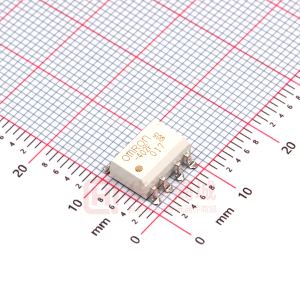
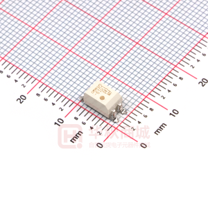
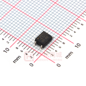
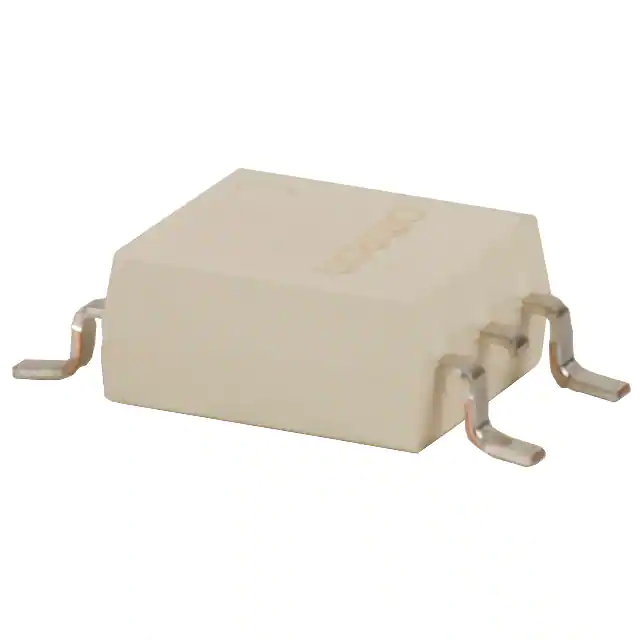
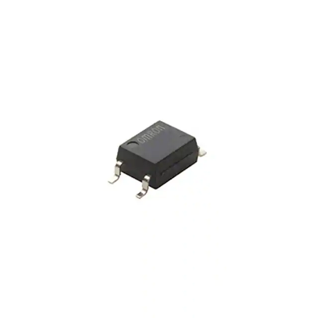
G3VM-41GR7TR

G3VM-41GR7TR

  • 厂商:

    OMRON(欧姆龙)

  • 封装:

  • 描述:

    G3VM-41GR7TR - MOS FET Relays - Omron Electronics LLC

  • 详情介绍
  • 数据手册
  • 价格&库存
G3VM-41GR7TR 数据手册
MOS FET Relays G3VM-41GR7 New MOS FET Relays with Low Output Capacitance and ON Resistance (C×R = 10.7pF•Ω) in a 40-V Load Voltage, SOP Package. • COFF = 1.65 pF (typical), RON = 6.5 Ω (typical) • Leakage current of 1.0 nA max. (0.2 nA typ.) when relay is open. • RoHS compliant ■ Application Examples • Semiconductor inspection tools • Measurement devices • Broadband systems • Data loggers Note: The actual product is marked differently from the image shown here. ■ List of Models Contact form SPST-NO Terminals Surface-mounting terminals Load voltage (peak value) 40 VAC Model G3VM-41GR7 G3VM-41GR7(TR) Number per stick 100 --Number per tape --2,500 ■ Dimensions Note: All units are in millimeters unless otherwise indicated. G3VM-41GR7 4.4±0.25 3.9±0.2 2.1 max. 0.15 Note: The actual product is marked differently from the image shown here. 0.4±0.1 2.54±0.25 0.1±0.1 0.6±0.3 7.0±0.4 Weight: 0.1 g ■ Terminal Arrangement/Internal Connections (Top View) G3VM-41GR7 4 3 1 2 ■ Actual Mounting Pad Dimensions (Recommended Value, Top View) G3VM-41GR7 6 to 6.3 1.2 0.8 2.54 MOS FET Relays G3VM-41GR7 113 ■ Absolute Maximum Ratings (Ta = 25°C) Item Input LED forward current LED forward current reduction rate LED reverse voltage Connection temperature Output Load voltage (AC peak/DC) Continuous load current ON current reduction rate Connection temperature Symbol IF Δ IF/°C VR Tj VOFF IO Δ IO/°C Tj 50 −0.5 5 125 40 120 −1.2 125 1,500 −20 to +85 Rating Unit mA mA/°C V °C V mA mA/°C °C Vrms °C AC for 1 min With no icing or condensation With no icing or condensation 10 s Ta ≥ 25°C Ta ≥ 25°C Measurement Conditions Note: 1. The dielectric strength between the input and output was checked by applying voltage between all pins as a group on the LED side and all pins as a group on the light-receiving side. Dielectric strength between input and VI-O output (See note 1.) Operating temperature Storage temperature Soldering temperature (10 s) Ta Tstg --- −40 to +125 °C 260 °C ■ Electrical Characteristics (Ta = 25°C) Item Input LED forward voltage Reverse current Capacity between terminals Trigger LED forward current Output Maximum resistance with output ON Symbol VF IR CT IFT RON Minimum 1.0 --------------1,000 ----Typical 1.15 --15 --6.5 0.2 1.65 0.8 --0.03 0.15 Maximum 1.3 10 --4 9.5 1.0 3.0 ----0.5 0.5 Unit V μA pF mA Ω nA pF pF MΩ ms ms Measurement conditions IF = 10 mA VR = 5 V V = 0, f = 1 MHz IO = 100 mA IF = 5 mA, IO = 120 mA, t = 10 ms VOFF = 30 V, Ta = 50°C V = 0, f = 100 MHz, t
G3VM-41GR7TR
### 物料型号 - 型号:G3VM-41GR7

### 器件简介 - 简介:新型MOS FET继电器,具有低输出电容和导通电阻(在40V负载电压下,$C_{OFF}=1.65\, \text{pF}$(典型值),$R_{ON}=6.5\, \Omega$(典型值))。漏电流最大为1.0纳安(典型值为0.2纳安)继电器开启时。符合RoHS标准。

### 引脚分配 - 接触形式:SPST-NO(单刀单掷-常开) - 终端:表面贴装端子

### 参数特性 - 绝对最大额定值: - 输入:LED正向电流50mA,LED反向电压5V - 输出:负载电压(AC峰值/DC)40V,连续负载电流120mA - 连接温度125°C - 电气特性: - LED正向电压:在5V、10mA条件下测量 - 最大电阻(输出ON):$R_{ON}$ 6.5Ω至9.5Ω - 继电器开启时的电流泄漏:0.2至1.0纳安 - 端子间电容:$C_{OFF}$ 1.65至3.0皮法 - I/O端子间电容:$C_{HO}$ 0.8皮法

### 功能详解 - 应用实例:半导体检测工具、测量设备、宽带系统、数据记录器。

### 应用信息 - 应用:适用于需要低输出电容和低导通电阻的场合,如半导体检测工具、测量设备等。

### 封装信息 - 封装:SOP封装 - 尺寸:所有单位均为毫米,具体尺寸图示请参考PDF文档中的图fig_29686、fig_07097等。

G3VM-41GR7TR 价格&库存

很抱歉,暂时无法提供与“G3VM-41GR7TR”相匹配的价格&库存,您可以联系我们找货

免费人工找货
G3VM-61VY2
  •  国内价格
  • 1+4.41931
  • 30+4.26692
  • 100+3.96214
  • 500+3.65736
  • 1000+3.50497

库存:0

G3VM-61VY2-TR
  •  国内价格
  • 1+7.0785
  • 10+5.94
  • 600+3.8808

库存:501

G3VM-402F
  •  国内价格
  • 1+8.6814
  • 10+8.3104

库存:17

G3VM-61D1(TR)
  •  国内价格
  • 1+7.81001
  • 30+7.53501
  • 100+6.98501
  • 500+6.435
  • 1000+6.16

库存:0

G3VM-61VY3(TR)
  •  国内价格
  • 1+5.78
  • 10+4.99
  • 50+4.36
  • 100+4.01
  • 500+3.61
  • 1000+3.33

库存:0