DATA SHEET
www.onsemi.com
Axial-Lead Glass
Passivated Standard
Recovery Rectifiers
STANDARD RECOVERY
RECTIFIERS
50−1000 VOLTS
3.0 AMPERES
1N5400 thru 1N5408
Lead mounted standard recovery rectifiers are designed for use in
power supplies and other applications having need of a device with the
following features:
Features
•
•
•
•
•
•
•
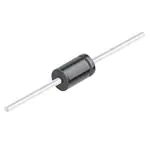
AXIAL LEAD
CASE 267−05
STYLE 1
High Current to Small Size
High Surge Current Capability
Low Forward Voltage Drop
Void−Free Economical Plastic Package
Available in Volume Quantities
Plastic Meets UL 94 V−0 for Flammability
These are Pb−Free Devices
MARKING DIAGRAM
Mechanical Characteristics:
• Case: Epoxy, Molded
• Weight: 1.1 Gram (Approximately)
• Finish: All External Surfaces Corrosion Resistant and Terminal
Leads are Readily Solderable
• Lead and Mounting Surface Temperature for Soldering Purposes:
•
260°C Max. for 10 Seconds
Polarity: Cathode Indicated by Polarity Band
A
1N
540x
YYWWG
G
A
= Assembly Location
1N540x = Device Number
x
= 0, 1, 2, 4, 6, 7 or 8
YY
= Year
WW
= Work Week
G
= Pb−Free Package
(Note: Microdot may be in either location)
ORDERING INFORMATION
See detailed ordering and shipping information on page 5 of
this data sheet.
*For additional information on our Pb−Free strategy and soldering details, please
download the onsemi Soldering and Mounting Techniques Reference Manual,
SOLDERRM/D.
© Semiconductor Components Industries, LLC, 2008
August, 2021 − Rev. 12
1
Publication Order Number:
1N5400/D
�1N5400 thru 1N5408
MAXIMUM RATINGS
Symbol
1N5400
1N5401
1N5402
1N5404
1N5406
1N5407
1N5408
Unit
Peak Repetitive Reverse Voltage
Working Peak Reverse Voltage
DC Blocking Voltage
Rating
VRRM
VRWM
VR
50
100
200
400
600
800
1000
V
Non−repetitive Peak Reverse Voltage
VRSM
100
200
300
525
800
1000
1200
V
Average Rectified Forward Current
(Single Phase Resistive Load,
1/2 in. Leads, TL = 105°C)
IO
3.0
A
Non−repetitive Peak Surge Current
(8 ms Single Half−Sine−Wave)
IFSM
200 (one cycle)
A
Operating and Storage Junction
Temperature Range
TJ
Tstg
− 65 to +150
− 65 to +175
°C
Stresses exceeding those listed in the Maximum Ratings table may damage the device. If any of these limits are exceeded, device functionality
should not be assumed, damage may occur and reliability may be affected.
THERMAL CHARACTERISTICS
Characteristic
Thermal Resistance, Junction−to−Ambient (PC Board Mount, 1/2 in. Leads)
Symbol
Typ
Unit
RqJA
53
°C/W
ELECTRICAL CHARACTERISTICS
Characteristic
Symbol
Min
Typ
Max
Unit
Forward Voltage (IF = 3.0 A, TA = 25°C)
vF
−
−
1.0
V
Reverse Current (Rated DC Voltage)
TA = 25°C
TA = 100°C
IR
−
−
−
−
10
50
mA
Product parametric performance is indicated in the Electrical Characteristics for the listed test conditions, unless otherwise noted. Product
performance may not be indicated by the Electrical Characteristics if operated under different conditions.
Ratings at 25°C ambient temperature unless otherwise specified.
60 Hz resistive or inductive loads.
For capacitive load, derate current by 20%.
www.onsemi.com
2
�1N5400 thru 1N5408
NOTE 1 — AMBIENT MOUNTING DATA
Data shown for thermal resistance junction−to−ambient (RqJA) for the
mountings shown is to be used as typical guideline values for preliminary
engineering or in case the tie point temperature cannot be measured.
TYPICAL VALUES FOR RqJA IN STILL AIR
Mounting
Method
1
2
Lead Length, L (IN)
1/8
1/4
1/2
3/4
55
51
53
50
63
59
61
58
°C/W
°C/W
3
28
°C/W
MOUNTING METHOD 1
P.C. Board Where Available
Copper Surface area is small
L
RqJA
MOUNTING METHOD 3
P.C. Board with
1−1/2” x 1−1/2”
Copper Surface
L
ÉÉÉÉÉÉÉÉÉ ÉÉ
ÉÉ
ÉÉ
ÉÉ
ÉÉ
L = 1/2”
MOUNTING METHOD 2
Vector Push−In Terminals T−28
Board Ground Plane
ÉÉÉÉÉÉÉÉÉ
L
L
www.onsemi.com
3
�1N5400 thru 1N5408
200
IFSM, PEAK HALF WAVE CURRENT (A)
400
TJ = 25°C
100
TYPICAL
50
30
20
200
1 CYCLE
100
90
80
70
60
50
40
1.0
5.0 7.0 10
2.0 3.0
20
50 70 100
30
10
NUMBER OF CYCLES
7.0
Figure 2. Maximum Nonrepetitive Surge Current
IF(AV), AVERAGE FORWARD CURRENT (A)
5.0
3.0
2.0
1.0
0.7
0.5
0.3
0.2
0.4
0.8
1.6
1.2
2.0
2.4
2.8
Square
Wave
1/4”
2
L = 1/32”
1/2”
1
50
60
70
80
90 100 110 120 130 140 150 160
Figure 3. Maximum Current Derating, Lead,
Various Lengths
4
DC
3
DC
2
Square
Wave
50
3
Figure 1. Forward Voltage
RqJA = 28°C/W
RqJA = 50°C/W
40
4
TL, LEAD TEMPERATURE (°C)
5
0
Both Leads to
Heat Sink
with Lengths
as Shown
DC
vF, INSTANTANEOUS VOLTAGE (V)
6
1
5
0
40
3.2
60
70
80
90 100 110 120 130 140 150 160
TA, AMBIENT TEMPERATURE (°C)
PF(AV), AVERAGE POWER DISSIPATION (W)
iF, INSTANTANEOUS FORWARD CURRENT (AMPS)
70
Surge Applied @
TJ = 25°C
f = 60 Hz
300
16
IPK/IAV = 20
14
5
10
Square
Wave
12
10
dc
8
6
4
2
0
TJ = 25°C
0
1
2
3
4
5
6
7
8
IF(AV), AVERAGE FORWARD CURRENT (A)
Figure 5. Forward Power Dissipation
Figure 4. Maximum Current Derating, Ambient, PC
Board Mounting
www.onsemi.com
4
9
10
�1N5400 thru 1N5408
ORDERING INFORMATION
Package
Shipping†
1N5400G
Axial Lead*
500 Units/Box
1N5400RLG
Axial Lead*
1200/Tape & Reel
1N5401G
Axial Lead*
500 Units/Box
1N5401RLG
Axial Lead*
1200/Tape & Reel
1N5402G
Axial Lead*
500 Units/Box
1N5402RLG
Axial Lead*
1200/Tape & Reel
1N5404G
Axial Lead*
500 Units/Box
1N5404RLG
Axial Lead*
1200/Tape & Reel
1N5406G
Axial Lead*
500 Units/Box
1N5406RLG
Axial Lead*
1200/Tape & Reel
1N5407G
Axial Lead*
500 Units/Box
1N5407RLG
Axial Lead*
1200/Tape & Reel
1N5408G
Axial Lead*
500 Units/Box
1N5408RLG
Axial Lead*
1200/Tape & Reel
Device
†For information on tape and reel specifications, including part orientation and tape sizes, please refer to our Tape and Reel Packaging
Specifications Brochure, BRD8011/D.
*This package is inherently Pb−Free.
www.onsemi.com
5
�MECHANICAL CASE OUTLINE
PACKAGE DIMENSIONS
AXIAL LEAD
CASE 267−05
ISSUE G
DATE 06/06/2000
SCALE 1:1
K
D
NOTES:
1. DIMENSIONS AND TOLERANCING PER ANSI
Y14.5M, 1982.
2. CONTROLLING DIMENSION: INCH.
3. 267-04 OBSOLETE, NEW STANDARD 267-05.
A
1
2
B
K
STYLE 1:
PIN 1. CATHODE (POLARITY BAND)
2. ANODE
DOCUMENT NUMBER:
DESCRIPTION:
DIM
A
B
D
K
98ASB42170B
AXIAL LEAD
INCHES
MIN
MAX
0.287
0.374
0.189
0.209
0.047
0.051
1.000
---
MILLIMETERS
MIN
MAX
7.30
9.50
4.80
5.30
1.20
1.30
25.40
---
STYLE 2:
NO POLARITY
Electronic versions are uncontrolled except when accessed directly from the Document Repository.
Printed versions are uncontrolled except when stamped “CONTROLLED COPY” in red.
PAGE 1 OF 1
ON Semiconductor and
are trademarks of Semiconductor Components Industries, LLC dba ON Semiconductor or its subsidiaries in the United States and/or other countries.
ON Semiconductor reserves the right to make changes without further notice to any products herein. ON Semiconductor makes no warranty, representation or guarantee regarding
the suitability of its products for any particular purpose, nor does ON Semiconductor assume any liability arising out of the application or use of any product or circuit, and specifically
disclaims any and all liability, including without limitation special, consequential or incidental damages. ON Semiconductor does not convey any license under its patent rights nor the
rights of others.
© Semiconductor Components Industries, LLC, 2019
www.onsemi.com
�onsemi,
, and other names, marks, and brands are registered and/or common law trademarks of Semiconductor Components Industries, LLC dba “onsemi” or its affiliates
and/or subsidiaries in the United States and/or other countries. onsemi owns the rights to a number of patents, trademarks, copyrights, trade secrets, and other intellectual property.
A listing of onsemi’s product/patent coverage may be accessed at www.onsemi.com/site/pdf/Patent−Marking.pdf. onsemi reserves the right to make changes at any time to any
products or information herein, without notice. The information herein is provided “as−is” and onsemi makes no warranty, representation or guarantee regarding the accuracy of the
information, product features, availability, functionality, or suitability of its products for any particular purpose, nor does onsemi assume any liability arising out of the application or use
of any product or circuit, and specifically disclaims any and all liability, including without limitation special, consequential or incidental damages. Buyer is responsible for its products
and applications using onsemi products, including compliance with all laws, regulations and safety requirements or standards, regardless of any support or applications information
provided by onsemi. “Typical” parameters which may be provided in onsemi data sheets and/or specifications can and do vary in different applications and actual performance may
vary over time. All operating parameters, including “Typicals” must be validated for each customer application by customer’s technical experts. onsemi does not convey any license
under any of its intellectual property rights nor the rights of others. onsemi products are not designed, intended, or authorized for use as a critical component in life support systems
or any FDA Class 3 medical devices or medical devices with a same or similar classification in a foreign jurisdiction or any devices intended for implantation in the human body. Should
Buyer purchase or use onsemi products for any such unintended or unauthorized application, Buyer shall indemnify and hold onsemi and its officers, employees, subsidiaries, affiliates,
and distributors harmless against all claims, costs, damages, and expenses, and reasonable attorney fees arising out of, directly or indirectly, any claim of personal injury or death
associated with such unintended or unauthorized use, even if such claim alleges that onsemi was negligent regarding the design or manufacture of the part. onsemi is an Equal
Opportunity/Affirmative Action Employer. This literature is subject to all applicable copyright laws and is not for resale in any manner.
PUBLICATION ORDERING INFORMATION
LITERATURE FULFILLMENT:
Email Requests to: orderlit@onsemi.com
onsemi Website: www.onsemi.com
◊
TECHNICAL SUPPORT
North American Technical Support:
Voice Mail: 1 800−282−9855 Toll Free USA/Canada
Phone: 011 421 33 790 2910
Europe, Middle East and Africa Technical Support:
Phone: 00421 33 790 2910
For additional information, please contact your local Sales Representative
�