Is Now Part of
To learn more about ON Semiconductor, please visit our website at
www.onsemi.com
Please note: As part of the Fairchild Semiconductor integration, some of the Fairchild orderable part numbers
will need to change in order to meet ON Semiconductor’s system requirements. Since the ON Semiconductor
product management systems do not have the ability to manage part nomenclature that utilizes an underscore
(_), the underscore (_) in the Fairchild part numbers will be changed to a dash (-). This document may contain
device numbers with an underscore (_). Please check the ON Semiconductor website to verify the updated
device numbers. The most current and up-to-date ordering information can be found at www.onsemi.com. Please
email any questions regarding the system integration to Fairchild_questions@onsemi.com.
ON Semiconductor and the ON Semiconductor logo are trademarks of Semiconductor Components Industries, LLC dba ON Semiconductor or its subsidiaries in the United States and/or other countries. ON Semiconductor owns the rights to a number
of patents, trademarks, copyrights, trade secrets, and other intellectual property. A listing of ON Semiconductor’s product/patent coverage may be accessed at www.onsemi.com/site/pdf/Patent-Marking.pdf. ON Semiconductor reserves the right
to make changes without further notice to any products herein. ON Semiconductor makes no warranty, representation or guarantee regarding the suitability of its products for any particular purpose, nor does ON Semiconductor assume any liability
arising out of the application or use of any product or circuit, and specifically disclaims any and all liability, including without limitation special, consequential or incidental damages. Buyer is responsible for its products and applications using ON
Semiconductor products, including compliance with all laws, regulations and safety requirements or standards, regardless of any support or applications information provided by ON Semiconductor. “Typical” parameters which may be provided in ON
Semiconductor data sheets and/or specifications can and do vary in different applications and actual performance may vary over time. All operating parameters, including “Typicals” must be validated for each customer application by customer’s
technical experts. ON Semiconductor does not convey any license under its patent rights nor the rights of others. ON Semiconductor products are not designed, intended, or authorized for use as a critical component in life support systems or any FDA
Class 3 medical devices or medical devices with a same or similar classification in a foreign jurisdiction or any devices intended for implantation in the human body. Should Buyer purchase or use ON Semiconductor products for any such unintended
or unauthorized application, Buyer shall indemnify and hold ON Semiconductor and its officers, employees, subsidiaries, affiliates, and distributors harmless against all claims, costs, damages, and expenses, and reasonable attorney fees arising out
of, directly or indirectly, any claim of personal injury or death associated with such unintended or unauthorized use, even if such claim alleges that ON Semiconductor was negligent regarding the design or manufacture of the part. ON Semiconductor
is an Equal Opportunity/Affirmative Action Employer. This literature is subject to all applicable copyright laws and is not for resale in any manner.
�1N4148WS, 1N4448WS,
1N914BWS
Small Signal Diodes
Features
•
•
•
•
•
•
•
General Purpose Diodes
Fast Switching Device (TRR < 4.0 ns)
Very Small and Thin SMD Package
Moisture Level Sensitivity 1
Matte Tin (Sn) Lead Finish
Green Mold Compound
Pb−free Version and RoHS Compliant
www.onsemi.com
T
2
ABSOLUTE MAXIMUM RATINGS
1
Symbol
Value
Unit
Non−Repetitive Peak Reverse Voltage
VRSM
100
V
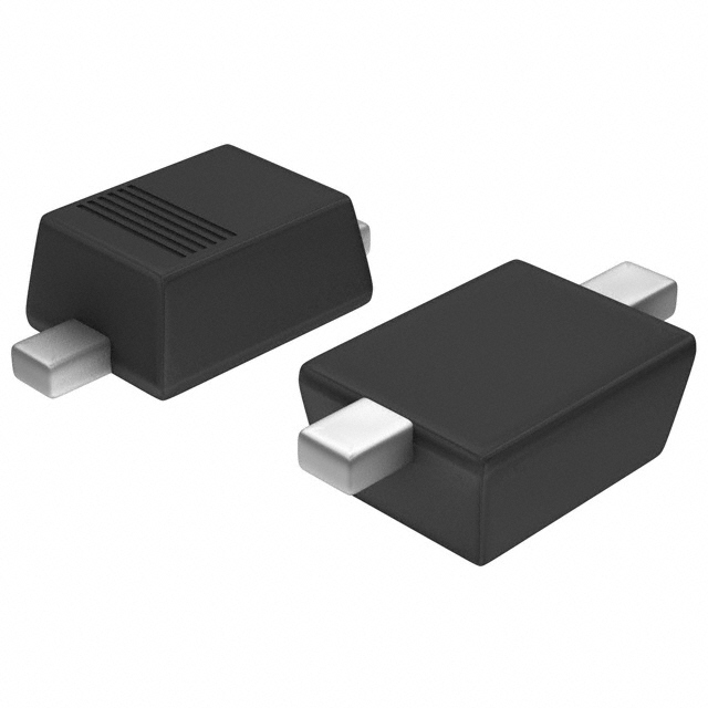
SOD−323
Flat Lead
CASE 477AB
Repetitive Peak Reverse Voltage
VRRM
75
V
Band Indicates Cathode
Repetitive Peak Forward Current
IFRM
300
mA
IO
150
mA
Parameter
Continuous Forward Current
Non−repetitive Peak Forward Surge
Current
Pulse Width = 1.0 s
Pulse Width = 1.0 ms
Operating Junction Temperature
Storage Temperature Range
IFSM
ELECTRICAL SYMBOL
A
1.0
4.0
(1)
Cathode
TJ
+150
°C
TSTG
−55 to +150
°C
(2)
Anode
Stresses exceeding those listed in the Maximum Ratings table may damage the
device. If any of these limits are exceeded, device functionality should not be
assumed, damage may occur and reliability may be affected.
ORDERING INFORMATION
Part Number
Top Mark
Package
Packing Method
1N4148WS
S1
SOD−323F 2L
Tape and Reel
1N4448WS
S2
SOD−323F 2L
Tape and Reel
1N914BWS
S3
SOD−323F 2L
Tape and Reel
© Semiconductor Components Industries, LLC, 2008
February, 2017 − Rev. 2
1
Publication Order Number:
1N4148WS/D
�1N4148WS, 1N4448WS, 1N914BWS
THERMAL CHARACTERISTICS (Values are at TA = 25°C unless otherwise noted.)
Parameter
Value
Unit
Power Dissipation (TC = 25°C)
200
mW
Thermal Resistance, Junction−to−Ambient (Note 1)
500
°C/W
Symbol
PD
RqJA
1. Device mounted on FR−4 PCB minimum land pad.
ELECTRICAL CHARACTERISTICS (Values are at TA = 25°C unless otherwise noted.)
Symbol
BVR
IR
VF
Parameter
Breakdown Voltage
Reverse Current
Forward Voltage
CO
Diode Capacitance
TRR
Reverse Recovery Time
Conditions
Min
IR = 100 mA
100
IR = 5 mA
75
Max
Unit
V
VR = 20 V
25
nA
VR = 75 V
5
mA
0.72
V
1N4448WS / 1N914BWS
IF = 5 mA
0.62
1N4148WS
IF = 10 mA
1
1N4448WS / 1N914BWS
IF = 100 mA
1
VR = 0, f = 1.0 MHz
4
pF
IF = 10 mA, IR = 60 mA,
IRR = 1 mA, RL = 100 W
4
ns
Product parametric performance is indicated in the Electrical Characteristics for the listed test conditions, unless otherwise noted. Product
performance may not be indicated by the Electrical Characteristics if operated under different conditions.
www.onsemi.com
2
�1N4148WS, 1N4448WS, 1N914BWS
TYPICAL CHARACTERISTICS
1.2
0.58
TA=25°C
0.56
Forward Voltage, VF [V]
1.0
Capacitance [pF]
0.54
0.52
0.50
0.48
0.8
o
TA= −40 C
0.6
o
TA= 25 C
0.4
o
TA= 85 C
0.2
0.46
o
TA= 150 C
0
0.44
0
2
4
6
8
10
12
0.01
14
0.1
1
10
100
1000
Forward Current, I F [mA]
Reverse Voltage (V)
Figure 2. Forward Voltage vs. Ambient Temperature
Figure 1. Total Capacitance
105
250
Reverse Current [nA]
PD − Power Dissipation [mW]
104 Ta=150°C
200
150
100
50
103
102
Ta=25°C
101
100
Ta=−40°C
0
0
25
50
75
100
125
150
10−1
175
10
Tem perature [°C]
40
50
60
70
80
90
Figure 4. Reverse Current vs. Reverse Voltage
170
Ta=25°C
VR − Reverse Voltage
30
Reverse Voltage, V R [V]
Figure 3. Power Derating Curve
160
150
140
1
20
10
100
Reverse Current, IR[μA]
Figure 5. Reverse Voltage vs. Reverse Current
www.onsemi.com
3
100
�1N4148WS, 1N4448WS, 1N914BWS
PACKAGE DIMENSIONS
SOD−323FL
CASE 477AB
ISSUE O
A
ON Semiconductor and
are trademarks of Semiconductor Components Industries, LLC dba ON Semiconductor or its subsidiaries in the United States and/or other countries.
ON Semiconductor owns the rights to a number of patents, trademarks, copyrights, trade secrets, and other intellectual property. A listing of ON Semiconductor’s product/patent
coverage may be accessed at www.onsemi.com/site/pdf/Patent−Marking.pdf. ON Semiconductor reserves the right to make changes without further notice to any products herein.
ON Semiconductor makes no warranty, representation or guarantee regarding the suitability of its products for any particular purpose, nor does ON Semiconductor assume any liability
arising out of the application or use of any product or circuit, and specifically disclaims any and all liability, including without limitation special, consequential or incidental damages.
Buyer is responsible for its products and applications using ON Semiconductor products, including compliance with all laws, regulations and safety requirements or standards,
regardless of any support or applications information provided by ON Semiconductor. “Typical” parameters which may be provided in ON Semiconductor data sheets and/or
specifications can and do vary in different applications and actual performance may vary over time. All operating parameters, including “Typicals” must be validated for each customer
application by customer’s technical experts. ON Semiconductor does not convey any license under its patent rights nor the rights of others. ON Semiconductor products are not
designed, intended, or authorized for use as a critical component in life support systems or any FDA Class 3 medical devices or medical devices with a same or similar classification
in a foreign jurisdiction or any devices intended for implantation in the human body. Should Buyer purchase or use ON Semiconductor products for any such unintended or unauthorized
application, Buyer shall indemnify and hold ON Semiconductor and its officers, employees, subsidiaries, affiliates, and distributors harmless against all claims, costs, damages, and
expenses, and reasonable attorney fees arising out of, directly or indirectly, any claim of personal injury or death associated with such unintended or unauthorized use, even if such
claim alleges that ON Semiconductor was negligent regarding the design or manufacture of the part. ON Semiconductor is an Equal Opportunity/Affirmative Action Employer. This
literature is subject to all applicable copyright laws and is not for resale in any manner.
PUBLICATION ORDERING INFORMATION
LITERATURE FULFILLMENT:
Literature Distribution Center for ON Semiconductor
19521 E. 32nd Pkwy, Aurora, Colorado 80011 USA
Phone: 303−675−2175 or 800−344−3860 Toll Free USA/Canada
Fax: 303−675−2176 or 800−344−3867 Toll Free USA/Canada
Email: orderlit@onsemi.com
◊
N. American Technical Support: 800−282−9855 Toll Free
USA/Canada
Europe, Middle East and Africa Technical Support:
Phone: 421 33 790 2910
Japan Customer Focus Center
Phone: 81−3−5817−1050
www.onsemi.com
4
ON Semiconductor Website: www.onsemi.com
Order Literature: http://www.onsemi.com/orderlit
For additional information, please contact your local
Sales Representative
1N4148WS/D
�ON Semiconductor and
are trademarks of Semiconductor Components Industries, LLC dba ON Semiconductor or its subsidiaries in the United States and/or other countries.
ON Semiconductor owns the rights to a number of patents, trademarks, copyrights, trade secrets, and other intellectual property. A listing of ON Semiconductor’s product/patent
coverage may be accessed at www.onsemi.com/site/pdf/Patent−Marking.pdf. ON Semiconductor reserves the right to make changes without further notice to any products herein.
ON Semiconductor makes no warranty, representation or guarantee regarding the suitability of its products for any particular purpose, nor does ON Semiconductor assume any liability
arising out of the application or use of any product or circuit, and specifically disclaims any and all liability, including without limitation special, consequential or incidental damages.
Buyer is responsible for its products and applications using ON Semiconductor products, including compliance with all laws, regulations and safety requirements or standards,
regardless of any support or applications information provided by ON Semiconductor. “Typical” parameters which may be provided in ON Semiconductor data sheets and/or
specifications can and do vary in different applications and actual performance may vary over time. All operating parameters, including “Typicals” must be validated for each customer
application by customer’s technical experts. ON Semiconductor does not convey any license under its patent rights nor the rights of others. ON Semiconductor products are not
designed, intended, or authorized for use as a critical component in life support systems or any FDA Class 3 medical devices or medical devices with a same or similar classification
in a foreign jurisdiction or any devices intended for implantation in the human body. Should Buyer purchase or use ON Semiconductor products for any such unintended or unauthorized
application, Buyer shall indemnify and hold ON Semiconductor and its officers, employees, subsidiaries, affiliates, and distributors harmless against all claims, costs, damages, and
expenses, and reasonable attorney fees arising out of, directly or indirectly, any claim of personal injury or death associated with such unintended or unauthorized use, even if such
claim alleges that ON Semiconductor was negligent regarding the design or manufacture of the part. ON Semiconductor is an Equal Opportunity/Affirmative Action Employer. This
literature is subject to all applicable copyright laws and is not for resale in any manner.
PUBLICATION ORDERING INFORMATION
LITERATURE FULFILLMENT:
Literature Distribution Center for ON Semiconductor
19521 E. 32nd Pkwy, Aurora, Colorado 80011 USA
Phone: 303−675−2175 or 800−344−3860 Toll Free USA/Canada
Fax: 303−675−2176 or 800−344−3867 Toll Free USA/Canada
Email: orderlit@onsemi.com
© Semiconductor Components Industries, LLC
N. American Technical Support: 800−282−9855 Toll Free
USA/Canada
Europe, Middle East and Africa Technical Support:
Phone: 421 33 790 2910
Japan Customer Focus Center
Phone: 81−3−5817−1050
www.onsemi.com
1
ON Semiconductor Website: www.onsemi.com
Order Literature: http://www.onsemi.com/orderlit
For additional information, please contact your local
Sales Representative
www.onsemi.com
�