ON Semiconductor
Is Now
To learn more about onsemi™, please visit our website at
www.onsemi.com
onsemi and and other names, marks, and brands are registered and/or common law trademarks of Semiconductor Components Industries, LLC dba “onsemi” or its affiliates and/or
subsidiaries in the United States and/or other countries. onsemi owns the rights to a number of patents, trademarks, copyrights, trade secrets, and other intellectual property. A listing of onsemi
product/patent coverage may be accessed at www.onsemi.com/site/pdf/Patent-Marking.pdf. onsemi reserves the right to make changes at any time to any products or information herein, without
notice. The information herein is provided “as-is” and onsemi makes no warranty, representation or guarantee regarding the accuracy of the information, product features, availability, functionality,
or suitability of its products for any particular purpose, nor does onsemi assume any liability arising out of the application or use of any product or circuit, and specifically disclaims any and all
liability, including without limitation special, consequential or incidental damages. Buyer is responsible for its products and applications using onsemi products, including compliance with all laws,
regulations and safety requirements or standards, regardless of any support or applications information provided by onsemi. “Typical” parameters which may be provided in onsemi data sheets and/
or specifications can and do vary in different applications and actual performance may vary over time. All operating parameters, including “Typicals” must be validated for each customer application
by customer’s technical experts. onsemi does not convey any license under any of its intellectual property rights nor the rights of others. onsemi products are not designed, intended, or authorized
for use as a critical component in life support systems or any FDA Class 3 medical devices or medical devices with a same or similar classification in a foreign jurisdiction or any devices intended for
implantation in the human body. Should Buyer purchase or use onsemi products for any such unintended or unauthorized application, Buyer shall indemnify and hold onsemi and its officers, employees,
subsidiaries, affiliates, and distributors harmless against all claims, costs, damages, and expenses, and reasonable attorney fees arising out of, directly or indirectly, any claim of personal injury or death
associated with such unintended or unauthorized use, even if such claim alleges that onsemi was negligent regarding the design or manufacture of the part. onsemi is an Equal Opportunity/Affirmative
Action Employer. This literature is subject to all applicable copyright laws and is not for resale in any manner. Other names and brands may be claimed as the property of others.
�Ordering number : EN4511D
1SV264
PIN Diode
http://onsemi.com
Dual series PIN Diode for VHF, UHF and AGC
50V, 50mA, rs=typ 2.5Ω, MCP
Features
•
•
•
Series connection of 2 elements in an ultlasmall package facilitates high-density mounting and
permits 1SV264-applied equipment to be made smaller
Small interterminal capacitance(C=0.23pF typ)
Small forward series resistance(rs=2.5Ω typ)
Specifications
Absolute Maximum Ratings at Ta=25°C
Parameter
Symbol
Conditions
Ratings
Unit
Reverse Voltage
VR
50
V
Forward Current
IF
50
mA
Allowable Power Dissipation
P
100
mW
Junction Temperature
Tj
125
°C
Storage Temperature
Tstg
--55 to +125
°C
Stresses exceeding Maximum Ratings may damage the device. Maximum Ratings are stress ratings only. Functional operation above the Recommended Operating
Conditions is not implied. Extended exposure to stresses above the Recommended Operating Conditions may affect device reliability.
Package Dimensions
Product & Package Information
unit : mm (typ)
7023A-007
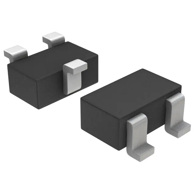
• Package
: MCP
• JEITA, JEDEC
: SC-70, SOT-323
• Minimum Packing Quantity : 3,000 pcs./reel
1SV264-TL-E
0.2
0.15
3
Packing Type: TL
Marking
0 to 0.08
1.25
2.1
0.425
2.0
LOT No.
2
0.65
0.9
LOT No.
TL
0.3
Electrical Connection
0.3
0.425
KV
1
1 : Anode
2 : Cathode
3 : Cathode / Anode
3
MCP
1
Semiconductor Components Industries, LLC, 2013
September, 2013
2
72512 TKIM/O1802 TSIM TA-100269/N0901 GIIM TA-3521/ No.4511-1/6
41098 HA (KT)/62096 GI/42294 YH (KOTO) BX-0219
�1SV264
Electrical Characteristics at Ta=25°C
Parameter
Reverse Voltage
Symbol
Forward Voltage
VR
IR
VF
Interterminal Capacitance
C
Series Resistance
rs
Reverse Current
Conditions
IR=10μA
VR=50V
Ratings
min
typ
max
50
V
0.1
IF=50mA
VR=50V, f=1MHz
Unit
μA
0.91
0.95
V
0.23
0.4
pF
IF=5mA, f=100MHz
4.0
8.0
Ω
IF=10mA, f=100MHz
2.5
4.5
Ω
Note : The specifications shown above are for each individual diode.
Ordering Information
Device
1SV264-TL-E
Package
Shipping
memo
MCP
3,000pcs./reel
Pb Free
No.4511-2/6
�1SV264
IF -- VF
Interterminal Capacitance, C -- pF
5°C
C
25°
C
--55°
1.0
7
5
3
2
0.1
7
5
3
2
0.2
0.4
0.6
0.8
1.0
Forward Voltage, VF -- V
1.2
5
3
2
2
3
5 7 1.0
2
2
3
5 7 100
ID00073
Ta=25°C
3
2
2
°C
=75
IF=10μA
Ta
10
1k
7
7
5
5
3
3
2
2
1.0
50°
Series Resistance, rs -- Ω
Reverse Current, IR -- nA
5 7 10
rs -- f
5
3
C
7
5
3
2
100μA
100
7
5
3
2
1mA
10
0.1
7
7
C
25°
5
5
5mA
3
3
10mA
2
2
0.01
10
0
20
30
40
50
Reverse Voltage, VR -- V
60
ID00074
1.0
1.0
2
3
5 7 10
2
3
5 7 100
2
Frequency, f -- MHz
3
5 7 1000 2
ID00075
rs -- IF
2
Ta=25°C
f=100MHz
1k
7
5
Series Resistance, rs -- Ω
3
Reverse Voltage, VR -- V
ID00072
IR -- VR
5
Ta=25°C
f=1MHz
7
0.1
0.1
0.01
0
C -- VR
1.0
10
7
5
3
2
Ta=
12
Forward Current, IF -- mA
5
3
2
3
2
100
7
5
3
2
10
7
5
3
2
1.0
0.01
2
3
5 7 0.1
2
3
5 7 1.0
Forward Current, IF -- mA
2
3
5 7 10
ID00076
No.4511-3/6
�1SV264
Embossed Taping Specification
1SV264-TL-E
No.4511-4/6
�1SV264
Outline Drawing
1SV264-TL-E
Land Pattern Example
Mass (g) Unit
0.006 mm
* For reference
Unit: mm
2.1
1.0
0.7
0.65 0.65
No.4511-5/6
�1SV264
ON Semiconductor and the ON logo are registered trademarks of Semiconductor Components Industries, LLC (SCILLC). SCILLC owns the rights to a number
of patents, trademarks, copyrights, trade secrets, and other intellectual property. A listing of SCILLC’s product/patent coverage may be accessed at
www.onsemi.com/site/pdf/Patent-Marking.pdf. SCILLC reserves the right to make changes without further notice to any products herein. SCILLC makes no
warranty, representation or guarantee regarding the suitability of its products for any particular purpose, nor does SCILLC assume any liability arising out of the
application or use of any product or circuit, and specifically disclaims any and all liability, including without limitation special, consequential or incidental
damages. “Typical” parameters which may be provided in SCILLC data sheets and/or specifications can and do vary in different applications and actual
performance may vary over time. All operating parameters, including “Typicals” must be validated for each customer application by customer’s technical
experts. SCILLC does not convey any license under its patent rights nor the rights of others. SCILLC products are not designed, intended, or authorized for use
as components in systems intended for surgical implant into the body, or other applications intended to support or sustain life, or for any other application in
which the failure of the SCILLC product could create a situation where personal injury or death may occur. Should Buyer purchase or use SCILLC products for
any such unintended or unauthorized application, Buyer shall indemnify and hold SCILLC and its officers, employees, subsidiaries, affiliates, and distributors
harmless against all claims, costs, damages, and expenses, and reasonable attorney fees arising out of, directly or indirectly, any claim of personal injury or
death associated with such unintended or unauthorized use, even if such claim alleges that SCILLC was negligent regarding the design or manufacture of the
part. SCILLC is an Equal Opportunity/Affirmative Action Employer. This literature is subject to all applicable copyright laws and is not for resale in any manner.
PS No.4511-6/6
�