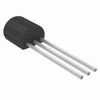
2N3663
E
TO-92
CB
NPN RF Transistor
This device is designed for use as RF amplifiers, oscillators and
multipliers with collector currents in the 1.0 mA to 30 mA range.
Sourced from Process 43. See PN918 for characteristics.
Absolute Maximum Ratings*
Symbol
TA = 25°C unless otherwise noted
Parameter
Value
Units
V
VCEO
Collector-Emitter Voltage
12
VCBO
Collector-Base Voltage
30
V
VEBO
Emitter-Base Voltage
3.0
V
IC
Collector Current - Continuous
50
mA
TJ, Tstg
Operating and Storage Junction Temperature Range
-55 to +150
°C
*These ratings are limiting values above which the serviceability of any semiconductor device may be impaired.
NOTES:
1) These ratings are based on a maximum junction temperature of 150 degrees C.
2) These are steady state limits. The factory should be consulted on applications involving pulsed or low duty cycle operations.
Thermal Characteristics
Symbol
PD
TA = 25°C unless otherwise noted
Characteristic
RθJC
Total Device Dissipation
Derate above 25°C
Thermal Resistance, Junction to Case
RθJA
Thermal Resistance, Junction to Ambient
© 1997 Fairchild Semiconductor Corporation
Max
Units
2N3663
350
2.8
125
mW
mW/°C
°C/W
357
°C/W
2N3663
Discrete POWER & Signal
Technologies
�(continued)
Electrical Characteristics
Symbol
TA = 25°C unless otherwise noted
Parameter
Test Conditions
Min
Max
Units
OFF CHARACTERISTICS
V(BR)CEO
Collector-Emitter Breakdown Voltage*
I C = 1.0 mA, IB = 0
12
V
V(BR)CBO
Collector-Base Breakdown Voltage
I C = 100 µA, IE = 0
30
V
V(BR)EBO
Emitter-Base Breakdown Voltage
I E = 100 µA, I C = 0
3.0
ICBO
Collector-Cutoff Current
VCB = 15 V, IE = 0
0.5
µA
IEBO
Emitter-Cutoff Current
VEB = 2.0 V, I C = 0
0.5
µA
MHz
V
ON CHARACTERISTICS*
hFE
DC Current Gain
VCE = 10 V, IC = 8.0 mA
20
IC = 5.0 mA, VCE = 10 V,
f = 100 MHz
VCB = 10 V, IE = 0, f = 1.0 MHz
700
2100
0.8
SMALL SIGNAL CHARACTERISTICS
fT
Current Gain - Bandwidth Product
Cob
Output Capacitance
rb’CC
Collector Base Time Constant
1.7
pF
IC = 8.0 mA, VCE = 10 V,
f = 79.8 MHz
80
pS
IC = 1.0 mA, VCE = 6.0 V,
f = 60 MHz, Rg = 400 Ω
IC = 6.0 mA, VCE = 12 V,
f = 200 MHz
6.5
dB
FUNCTIONAL TEST
NF
Noise Figure
Gpe
Amplifier Power Gain
*Pulse Test: Pulse Width ≤ 300 µs, Duty Cycle ≤ 2.0%
1.5
dB
2N3663
NPN RF Transistor
�
很抱歉,暂时无法提供与“2N3663”相匹配的价格&库存,您可以联系我们找货
免费人工找货