DATA SHEET
www.onsemi.com
N-Channel Enhancement
Mode Field Effect
Transistor
D
G
2N7000, 2N7002,
NDS7002A
S
Description
These N−channel enhancement mode field effect transistors are
produced using onsemi’s proprietary, high cell density, DMOS
technology. These products have been designed to minimize on−state
resistance while providing rugged, reliable, and fast switching
performance. They can be used in most applications requiring up to
400 mAdc and can deliver pulsed currents up to 2 A. These products
are particularly suited for low−voltage, low−current applications, such
as small servo motor control, power MOSFET gate drivers, and other
switching applications.
1 − Source
2 − Gate
3 − Drain
12
2
3
TO−92
CASE 135AR
TO−92
CASE 135AN
MARKING DIAGRAM
Features
•
•
•
•
•
1
3
High Density Cell Design for Low RDS(on)
Voltage Controlled Small Signal Switch
Rugged and Reliable
High Saturation Current Capability
This Device is Pb−Free and Halogen Free
$Y&Z&3
2N
7000
$Y
&Z
&3
2N7000
= Logo
= Assembly Plant Code
= Date Code
= Specific Device Code
3
1 − Gate
2 − Source
3 − Drain
1
2
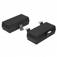
SOT−23
CASE 318−08
MARKING DIAGRAM
&E&Y
7x2&E&G
&E
&Y
7x2
&G
= Designates Space
= Binary Calendar Year Coding Scheme
= Specific Device Code
x= 0, 1
= Date Code
ORDERING INFORMATION
See detailed ordering and shipping information on page 7 of
this data sheet.
© Semiconductor Components Industries, LLC, 1998
July, 2022 − Rev. 7
1
Publication Order Number:
NDS7002A/D
�2N7000, 2N7002, NDS7002A
ABSOLUTE MAXIMUM RATINGS Values are at TC = 25°C unless otherwise noted.
Value
Symbol
2N7000
Parameter
2N7002
NDS7002A
Unit
VDSS
Drain−to−Source Voltage
60
V
VDGR
Drain−Gate Voltage (RGS ≤ 1 MW)
60
V
VGSS
Gate−Source Voltage − Continuous
±20
V
Gate−Source Voltage − Non Repetitive (tp < 50 ms)
±40
ID
PD
TJ, TSTG
TL
mA
Maximum Drain Current − Continuous
200
115
280
Maximum Drain Current − Pulsed
500
800
1500
Maximum Power Dissipation Derated above 25°C
400
200
300
mW
3.2
1.6
2.4
mW/°C
−65 to 150
°C
Operating and Storage Temperature Range
−55 to 150
Maximum Lead Temperature for Soldering Purposes,
1/16−inch from Case for 10 s
300
°C
Stresses exceeding those listed in the Maximum Ratings table may damage the device. If any of these limits are exceeded, device functionality
should not be assumed, damage may occur and reliability may be affected.
THERMAL CHARACTERISTICS Values are at TC = 25°C unless otherwise noted.
Value
Symbol
RθJA
Parameter
Thermal Resistance, Junction to Ambient
2N7000
2N7002
NDS7002A
Unit
312.5
625
417
°C/W
ELECTRICAL CHARACTERISTICS
Values are at TC = 25°C unless otherwise noted.
Symbol
Parameter
Conditions
Type
Min
Typ
Max
Unit
V
OFF CHARACTERISTICS
BVDSS
IDSS
Drain−Source Breakdown
Voltage
VGS = 0 V, ID = 10 mA
All
60
−
−
Zero Gate Voltage Drain
Current
VDS = 48 V, VGS = 0 V
2N7000
−
−
1
mA
−
−
1
mA
2N7002
NDS7002A
−
−
1
mA
−
−
0.5
mA
nA
VDS = 48 V, VGS = 0 V,
TC = 125°C
VDS = 60 V, VGS = 0 V
VDS = 60 V, VGS = 0 V,
TC = 125°C
IGSSF
IGSSR
Gate − Body Leakage,
Forward
VGS = 15 V, VDS = 0 V
2N7000
−
−
10
VGS = 20 V, VDS = 0 V
2N7002
NDS7002A
−
−
100
Gate − Body Leakage,
Reverse
VGS = −15 V, VDS = 0 V
2N7000
−
−
−10
VGS = −20 V, VDS = 0 V
2N7002
NDS7002A
−
−
−100
2N7000
0.8
2.1
3
2N7002
NDS7002A
1
2.1
2.5
nA
ON CHARACTERISTICS
VGS(th)
Gate Threshold Voltage
VDS = VGS, ID = 1 mA
VDS = VGS, ID = 250 mA
www.onsemi.com
2
V
�2N7000, 2N7002, NDS7002A
ELECTRICAL CHARACTERISTICS (continued)
Values are at TC = 25°C unless otherwise noted.
Symbol
Parameter
Conditions
Type
Min
Typ
Max
Unit
2N7000
−
1.2
5
W
VGS = 10 V, ID = 500 mA,
TC = 125°C
−
1.9
9
VGS = 4.5 V, ID = 75 mA
−
1.8
5.3
−
1.2
7.5
VGS = 10 V, ID = 500 mA,
TC = 100°C
−
1.7
13.5
VGS = 5 V, ID = 50 mA
−
1.7
7.5
VGS = 5 V, ID = 50 mA,
TC = 100°C
−
2.4
13.5
−
1.2
2
VGS = 10 V, ID = 500 mA,
TC = 125°C
−
2
3.5
VGS = 5 V, ID = 50 mA
−
1.7
3
VGS = 5 V, ID = 50 mA,
TC = 125°C
−
2.8
5
−
0.6
2.5
−
0.14
0.4
−
0.6
3.75
−
0.09
1.5
−
0.6
1
−
0.09
0.15
ON CHARACTERISTICS
RDS(on)
Static Drain−Source
On−Resistance
VGS = 10 V, ID = 500 mA
VGS = 10 V, ID = 500 mA
VGS = 10 V, ID = 500 mA
VDS(on)
Drain−Source On−Voltage
VGS = 10 V, ID = 500 mA
2N7002
NDS7002A
2N7000
VGS = 4.5 V, ID = 75 mA
VGS = 10 V, ID = 500 mA
2N7002
VGS = 5.0 V, ID = 50 mA
VGS = 10 V, ID = 500 mA
NDS7002A
VGS = 5.0 V, ID = 50 mA
ID(on)
gFS
On−State Drain Current
Forward Transconductance
VGS = 4.5 V, VDS = 10 V
2N7000
75
600
−
VGS = 10 V, VDS ≥ 2 VDS(on)
2N7002
500
2700
−
VGS = 10 V, VDS ≥ 2 VDS(on)
NDS7002A
500
2700
−
VDS = 10 V, ID = 200 mA
2N7000
100
320
−
VDS ≥ 2 VDS(on), ID = 200 mA
2N7002
80
320
−
VDS ≥ 2 VDS(on), ID = 200 mA
NDS7002A
80
320
−
All
−
20
50
All
−
11
25
All
−
4
5
VDD = 15 V, RL = 25 W,
ID = 500 mA, VGS = 10 V,
RGEN = 25 W
2N7000
−
−
VDD = 30 V, RL = 150 W,
ID = 200 mA, VGS = 10 V,
RGEN = 25 W
2N7002
NDS7002A
−
VDD = 15 V, RL = 25 W,
ID = 500 mA, VGS = 10 V,
RGEN = 25 W
2N7000
−
VDD = 30 V, RL = 150 W,
ID = 200 mA, VGS = 10 V,
RGEN = 25 W
2N7002
NDS7002A
V
mA
mS
DYNAMIC CHARACTERISTICS
Ciss
Input Capacitance
Coss
Output Capacitance
Crss
Reverse Transfer
Capacitance
ton
toff
Turn−On Time
Turn−Off Time
VDS = 25 V, VGS = 0 V,
f = 1.0 MHz
www.onsemi.com
3
pF
ns
10
−
20
ns
−
10
−
−
20
�2N7000, 2N7002, NDS7002A
ELECTRICAL CHARACTERISTICS (continued)
Values are at TC = 25°C unless otherwise noted.
Symbol
Parameter
Conditions
Type
Min
Typ
Max
Unit
2N7002
−
−
115
mA
NDS7002A
−
−
280
2N7002
−
−
0.8
NDS7002A
−
−
1.5
VGS = 0 V, IS = 115 mA
(Note 1)
2N7002
−
0.88
1.5
VGS = 0 V, IS = 400 mA
(Note 1)
NDS7002A
−
0.88
1.2
DRAIN−SOURCE DIODE CHARACTERISTICS AND MAXIMUM RATINGS
IS
Maximum Continuous Drain−Source Diode Forward Current
ISM
Maximum Pulsed Drain−Source Diode Forward Current
VSD
Drain−Source Diode
Forward Voltage
A
V
Product parametric performance is indicated in the Electrical Characteristics for the listed test conditions, unless otherwise noted. Product
performance may not be indicated by the Electrical Characteristics if operated under different conditions.
1. Pulse test: Pulse Width ≤ 300 ms, Duty Cycel ≤ 2 %
TYPICAL PERFORMANCE CHARACTERISTICS
3
9.0
8.0
VGS = 10 V
7.0
RDS(on), Normalized
Drain−Source On−Resistance
ID, Drain−Source Current (A)
2
1.5
6.0
1
5.0
4.0
0.5
3.0
0
1
2
3
4
7.0
8.0
1.5
9.0
10
1
0
0.4
0.8
1.2
1.6
ID, Drain Current (A)
Figure 1. On−Region Characteristics
Figure 2. On−Resistance Variation with
Gate Voltage and Drain Current
2
3
VGS = 10 V
ID = 500 mA
RDS(on), Normalized
Drain−Source On−Resistance
RDS(on), Normalized
Drain−Source On−Resistance
6.0
VDS, Drain−Source Voltage (V)
1.5
1.25
1
0.75
0.5
−50
5.0
2
5
2
1.75
4.5
2.5
0.5
0
V = 4.0
−25
0
25
50
75
100
125
150
VGS
2.5
TJ = 125°C
2
1.5
25°C
1
−55°C
0.5
0
0
TJ, Junction Temperature (5C)
0.4
0.8
1.2
1.6
ID, Drain Current (A)
Figure 3. On−Resistance Variation with
Temperature
Figure 4. On−Resistance Variation with
Drain Current and Temperature
www.onsemi.com
4
2
�2N7000, 2N7002, NDS7002A
TYPICAL PERFORMANCE CHARACTERISTICS (Continued)
2
125°C
T = −55°C
1.2
0.8
0.4
Vth, Normalized Gate−Source
Threshold Voltage
1.6
ID, Drain Current (A)
1.1
25°C
VDS = 10 V
0
0
2
4
6
8
1
0.95
0.9
0.85
0.8
−50
10
25
50
75
100
125
Figure 5. Transfer Characteristics
Figure 6. Gate Threshold Variation with
Temperature
2
IS, Reverse Drain Current (A)
1.050
1.025
1.000
0.975
150
VGS = 0 V
1
0.5
T = 125°C
0.1
25°C
0.05
−55°C
0.01
0.005
0.950
0.925
−50
−25
0
25
50
75
100
TJ, Junction Temperature (5C)
125
150
0.001
0.2
Figure 7. Breakdown Voltage Variation with
Temperature
10
VGS, GA E−Source Voltage (V)
40
Ciss
20
Coss
10
5
Crss
2
1
f = 1 MHz
V=0V
1
2
3
5
10
20
30
1.2
0.4
0.6
0.8
1
VSD, Body Diode Forward Voltage (V)
1.4
Figure 8. Body Diode Forward Voltage
Variation with
60
Capacitance (pF)
0
TJ, Junction Temperature (5C)
ID = 250 mA
1.075
−25
VGS, Gate to Source Voltage (V)
1.100
BVDSS, Normalized
Drain−Source Breakdown Voltage
VDS = VGS
I = 1 mA
1.05
50
VDS = 25 V
8
6
I = 500 mA
4
280 mA
2
115 mA
0
0
0.4
0.8
1.2
1.6
VDS, Drain to Source Voltage (V)
Qg, Gate Charge (nC)
Figure 9. Capacitance Characteristics
Figure 10. Gate Charge Characteristics
www.onsemi.com
5
2
�2N7000, 2N7002, NDS7002A
TYPICAL PERFORMANCE CHARACTERISTICS (Continued)
ton
VDD
td(on)
RL
VIN
RGEN
tf
90%
90%
Output, Vout
DUT
G
td(off)
tr
VOUT
D
VGS
toff
10%
10%
90%
S
50%
50%
Input, Vin
10%
Inverted
Pulse Width
Figure 11. Switching Test Circuit
Figure 12. Switching Waveforms
3
2
3
2
100 ms
1 ms
0.1
100 ms
10 ms
0.05
1s
VGS = 10 V
Single Pulse
TA = 25°C
0.01
0.005
1
2
10 s
ID, Drain Current (A)
0.5
100 ms
1
RDS(on) Limit
DS
5
10
20
RDS(on) Limit
0.5
60 80
0.05
0.005
VGS = 10 V
Single Pulse
TA = 25°C
1
DC
2
5
RDS(on) Limit
100 ms
1 ms
0.5
10 ms
0.1
100 ms
0.05
0.005
1s
VGS = 10 V
Single Pulse
TA = 25°C
1
2
20
1s
30
60 80
Figure 14. 2N7002 Maximum Safe Operating Area
1
0.01
10
10 s
VDS, Drain−Source Voltage (V)
Figure 13. 2N7000 Maximum Safe Operating Area
3
2
10 ms
100 ms
0.01
30
1 ms
0.1
VDS, Drain−Source Voltage (V)
ID, Drain Current (A)
ID, Drain Current (A)
1
DC
5
10
20
10 s
30
60 80
VDS, Drain−Source Voltage (V)
Figure 15. NDS7000A Maximum Safe Operating Area
www.onsemi.com
6
�2N7000, 2N7002, NDS7002A
TYPICAL PERFORMANCE CHARACTERISTICS (Continued)
r(t), Normalized Effective
Transient Thermal Resistance
1
0.5
0.2
0.1
0.05
0.02
0.01
D = 0.5
0.2
RqJA(t) = r(t) * RqJA
RqJA = (See Datasheet)
0.1
0.05
P(pk)
t1
0.02
0.01
Single Pulse
0.0001
t2
TJ − TA = P * RqJA(t)
Duty Cycle, D = t1/t2
0.001
0.01
0.1
1
10
100
300
t1, Time (s)
Figure 16. TO−92, 2N7000 Transient Thermal Response Curve
r(t), Normalized Effective
Transient Thermal Resistance
1
0.5
0.2
D = 0.5
0.2
0.1
0.1
0.05
0.05
RqJA(t) = r(t) * RqJA
RqJA = (See Datasheet)
P(pk)
0.02
0.01
0.002
0.001
t1
0.01
TJ − TA = P * RqJA(t)
Duty Cycle, D = t1/t2
Single Pulse
0.0001
t2
0.001
0.01
0.1
1
10
100
300
t1, Time (s)
Figure 17. SOT−23, 2N7002 / NDS7002A Transient Thermal Response Curve
ORDERING INFORMATION
Part Number
Marking
Package
Packing Method†
Min Order Qty /
Immediate Pack Qty
2N7000
2N7000
TO−92 3L
(Pb−Free)
Bulk
10000 / 1000
Ammo
2000 / 2000
Tape and Reel
2000 / 2000
2N7000−D74Z
2N7000−D75Z
2N7000−D26Z
2000 / 2000
2N7002
702
NDS7002A
712
SOT−23 3L
(Pb−Free)
Tape and Reel
3000 / 3000
3000 / 3000
†For information on tape and reel specifications, including part orientation and tape sizes, please refer to our Tape and Reel Packaging
Specifications Brochure, BRD8011/D.
www.onsemi.com
7
�MECHANICAL CASE OUTLINE
PACKAGE DIMENSIONS
TO−92 3 4.825x4.76
CASE 135AN
ISSUE O
DOCUMENT NUMBER:
DESCRIPTION:
98AON13880G
TO−92 3 4.825X4.76
DATE 31 JUL 2016
Electronic versions are uncontrolled except when accessed directly from the Document Repository.
Printed versions are uncontrolled except when stamped “CONTROLLED COPY” in red.
PAGE 1 OF 1
ON Semiconductor and
are trademarks of Semiconductor Components Industries, LLC dba ON Semiconductor or its subsidiaries in the United States and/or other countries.
ON Semiconductor reserves the right to make changes without further notice to any products herein. ON Semiconductor makes no warranty, representation or guarantee regarding
the suitability of its products for any particular purpose, nor does ON Semiconductor assume any liability arising out of the application or use of any product or circuit, and specifically
disclaims any and all liability, including without limitation special, consequential or incidental damages. ON Semiconductor does not convey any license under its patent rights nor the
rights of others.
© Semiconductor Components Industries, LLC, 2019
www.onsemi.com
�MECHANICAL CASE OUTLINE
PACKAGE DIMENSIONS
TO−92 3 4.83x4.76 LEADFORMED
CASE 135AR
ISSUE O
DOCUMENT NUMBER:
DESCRIPTION:
98AON13879G
DATE 30 SEP 2016
Electronic versions are uncontrolled except when accessed directly from the Document Repository.
Printed versions are uncontrolled except when stamped “CONTROLLED COPY” in red.
TO−92 3 4.83X4.76 LEADFORMED
PAGE 1 OF 1
ON Semiconductor and
are trademarks of Semiconductor Components Industries, LLC dba ON Semiconductor or its subsidiaries in the United States and/or other countries.
ON Semiconductor reserves the right to make changes without further notice to any products herein. ON Semiconductor makes no warranty, representation or guarantee regarding
the suitability of its products for any particular purpose, nor does ON Semiconductor assume any liability arising out of the application or use of any product or circuit, and specifically
disclaims any and all liability, including without limitation special, consequential or incidental damages. ON Semiconductor does not convey any license under its patent rights nor the
rights of others.
© Semiconductor Components Industries, LLC, 2019
www.onsemi.com
�MECHANICAL CASE OUTLINE
PACKAGE DIMENSIONS
SOT−23 (TO−236)
CASE 318−08
ISSUE AS
DATE 30 JAN 2018
SCALE 4:1
D
0.25
3
E
1
2
T
HE
NOTES:
1. DIMENSIONING AND TOLERANCING PER ASME Y14.5M, 1994.
2. CONTROLLING DIMENSION: MILLIMETERS.
3. MAXIMUM LEAD THICKNESS INCLUDES LEAD FINISH.
MINIMUM LEAD THICKNESS IS THE MINIMUM THICKNESS OF
THE BASE MATERIAL.
4. DIMENSIONS D AND E DO NOT INCLUDE MOLD FLASH,
PROTRUSIONS, OR GATE BURRS.
DIM
A
A1
b
c
D
E
e
L
L1
HE
T
L
3X b
L1
VIEW C
e
TOP VIEW
A
A1
SIDE VIEW
SEE VIEW C
c
MIN
0.89
0.01
0.37
0.08
2.80
1.20
1.78
0.30
0.35
2.10
0°
MILLIMETERS
NOM
MAX
1.00
1.11
0.06
0.10
0.44
0.50
0.14
0.20
2.90
3.04
1.30
1.40
1.90
2.04
0.43
0.55
0.54
0.69
2.40
2.64
−−−
10 °
MIN
0.035
0.000
0.015
0.003
0.110
0.047
0.070
0.012
0.014
0.083
0°
INCHES
NOM
0.039
0.002
0.017
0.006
0.114
0.051
0.075
0.017
0.021
0.094
−−−
MAX
0.044
0.004
0.020
0.008
0.120
0.055
0.080
0.022
0.027
0.104
10°
GENERIC
MARKING DIAGRAM*
END VIEW
RECOMMENDED
SOLDERING FOOTPRINT
XXXMG
G
1
3X
2.90
3X
XXX = Specific Device Code
M = Date Code
G
= Pb−Free Package
0.90
*This information is generic. Please refer to
device data sheet for actual part marking.
Pb−Free indicator, “G” or microdot “ G”,
may or may not be present.
0.95
PITCH
0.80
DIMENSIONS: MILLIMETERS
STYLE 1 THRU 5:
CANCELLED
STYLE 6:
PIN 1. BASE
2. EMITTER
3. COLLECTOR
STYLE 7:
PIN 1. EMITTER
2. BASE
3. COLLECTOR
STYLE 9:
PIN 1. ANODE
2. ANODE
3. CATHODE
STYLE 10:
PIN 1. DRAIN
2. SOURCE
3. GATE
STYLE 11:
STYLE 12:
PIN 1. ANODE
PIN 1. CATHODE
2. CATHODE
2. CATHODE
3. CATHODE−ANODE
3. ANODE
STYLE 15:
PIN 1. GATE
2. CATHODE
3. ANODE
STYLE 16:
PIN 1. ANODE
2. CATHODE
3. CATHODE
STYLE 17:
PIN 1. NO CONNECTION
2. ANODE
3. CATHODE
STYLE 18:
STYLE 19:
STYLE 20:
PIN 1. NO CONNECTION PIN 1. CATHODE
PIN 1. CATHODE
2. CATHODE
2. ANODE
2. ANODE
3. GATE
3. ANODE
3. CATHODE−ANODE
STYLE 21:
PIN 1. GATE
2. SOURCE
3. DRAIN
STYLE 22:
PIN 1. RETURN
2. OUTPUT
3. INPUT
STYLE 23:
PIN 1. ANODE
2. ANODE
3. CATHODE
STYLE 24:
PIN 1. GATE
2. DRAIN
3. SOURCE
STYLE 27:
PIN 1. CATHODE
2. CATHODE
3. CATHODE
STYLE 28:
PIN 1. ANODE
2. ANODE
3. ANODE
DOCUMENT NUMBER:
DESCRIPTION:
98ASB42226B
SOT−23 (TO−236)
STYLE 8:
PIN 1. ANODE
2. NO CONNECTION
3. CATHODE
STYLE 13:
PIN 1. SOURCE
2. DRAIN
3. GATE
STYLE 25:
PIN 1. ANODE
2. CATHODE
3. GATE
STYLE 14:
PIN 1. CATHODE
2. GATE
3. ANODE
STYLE 26:
PIN 1. CATHODE
2. ANODE
3. NO CONNECTION
Electronic versions are uncontrolled except when accessed directly from the Document Repository.
Printed versions are uncontrolled except when stamped “CONTROLLED COPY” in red.
PAGE 1 OF 1
ON Semiconductor and
are trademarks of Semiconductor Components Industries, LLC dba ON Semiconductor or its subsidiaries in the United States and/or other countries.
ON Semiconductor reserves the right to make changes without further notice to any products herein. ON Semiconductor makes no warranty, representation or guarantee regarding
the suitability of its products for any particular purpose, nor does ON Semiconductor assume any liability arising out of the application or use of any product or circuit, and specifically
disclaims any and all liability, including without limitation special, consequential or incidental damages. ON Semiconductor does not convey any license under its patent rights nor the
rights of others.
© Semiconductor Components Industries, LLC, 2019
www.onsemi.com
�onsemi,
, and other names, marks, and brands are registered and/or common law trademarks of Semiconductor Components Industries, LLC dba “onsemi” or its affiliates
and/or subsidiaries in the United States and/or other countries. onsemi owns the rights to a number of patents, trademarks, copyrights, trade secrets, and other intellectual property.
A listing of onsemi’s product/patent coverage may be accessed at www.onsemi.com/site/pdf/Patent−Marking.pdf. onsemi reserves the right to make changes at any time to any
products or information herein, without notice. The information herein is provided “as−is” and onsemi makes no warranty, representation or guarantee regarding the accuracy of the
information, product features, availability, functionality, or suitability of its products for any particular purpose, nor does onsemi assume any liability arising out of the application or use
of any product or circuit, and specifically disclaims any and all liability, including without limitation special, consequential or incidental damages. Buyer is responsible for its products
and applications using onsemi products, including compliance with all laws, regulations and safety requirements or standards, regardless of any support or applications information
provided by onsemi. “Typical” parameters which may be provided in onsemi data sheets and/or specifications can and do vary in different applications and actual performance may
vary over time. All operating parameters, including “Typicals” must be validated for each customer application by customer’s technical experts. onsemi does not convey any license
under any of its intellectual property rights nor the rights of others. onsemi products are not designed, intended, or authorized for use as a critical component in life support systems
or any FDA Class 3 medical devices or medical devices with a same or similar classification in a foreign jurisdiction or any devices intended for implantation in the human body. Should
Buyer purchase or use onsemi products for any such unintended or unauthorized application, Buyer shall indemnify and hold onsemi and its officers, employees, subsidiaries, affiliates,
and distributors harmless against all claims, costs, damages, and expenses, and reasonable attorney fees arising out of, directly or indirectly, any claim of personal injury or death
associated with such unintended or unauthorized use, even if such claim alleges that onsemi was negligent regarding the design or manufacture of the part. onsemi is an Equal
Opportunity/Affirmative Action Employer. This literature is subject to all applicable copyright laws and is not for resale in any manner.
PUBLICATION ORDERING INFORMATION
LITERATURE FULFILLMENT:
Email Requests to: orderlit@onsemi.com
onsemi Website: www.onsemi.com
◊
TECHNICAL SUPPORT
North American Technical Support:
Voice Mail: 1 800−282−9855 Toll Free USA/Canada
Phone: 011 421 33 790 2910
Europe, Middle East and Africa Technical Support:
Phone: 00421 33 790 2910
For additional information, please contact your local Sales Representative
�


 工商网监
湘ICP备2023018690号
工商网监
湘ICP备2023018690号
