DATA SHEET
www.onsemi.com
NPN Epitaxial Silicon
Transistor
FJL4315, 2SC5200
Features
•
•
•
•
•
•
•
•
•
•
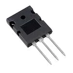
1. Base
2. Collector
3. Emitter
1
High Current Capability: IC = 17 A
High Power Dissipation: 150 W
High Frequency: 30 MHz
High Voltage: VCEO = 250 V
Wide S.O.A. for Reliable Operation
Excellent Gain Linearity for Low THD
Complement to 2SA1943 / FJL4215
Thermal and Electrical Spice Models are Available
Same Transistor is also Available in:
♦ TO3P Package, 2SC5242 / FJA4313 : 130 Watts
♦ TO220 Package, FJP5200 : 80 Watts
♦ TO220F Package, FJPF5200 : 50 Watts
These Devices are Pb−Free and are RoHS Compliant
TO−264−3LD
CASE 340CA
MARKING DIAGRAM
Logo
AYWWZZ
XXXXXX
XXXXXX
Applications
• High−Fidelity Audio Output Amplifier
• General Purpose Power Amplifier
ABSOLUTE MAXIMUM RATINGS (TA = 25°C unless otherwise noted)
Parameter
Symbol
Ratings
Units
Collector−Base Voltage
BVCBO
250
V
Collector−Emitter Voltage
BVCEO
250
V
Emitter−Base Voltage
BVEBO
5
V
Collector Current (DC)
IC
17
A
Base Current
IB
1.5
A
Total Device Dissipation (TC = 25°C)
Derate Above 25°C
PD
150
1.04
W
W/°C
TJ, TSTG
−50 ~ +150
°C
Junction and Storage Temperature
A
YWW
ZZ
xxxxx
= Assembly Location
= Date Code
= Assembly Lot
= Specific Device Code
(J4315O or C5200O)
ORDERING INFORMATION
See detailed ordering and shipping information on page 2 of
this data sheet.
Stresses exceeding those listed in the Maximum Ratings table may damage the
device. If any of these limits are exceeded, device functionality should not be
assumed, damage may occur and reliability may be affected.
THERMAL CHARACTERISTICS (Note 1)
(TA = 25°C unless otherwise noted)
Parameter
Thermal Resistance, Junction to Case
Symbol
Max.
Units
RqJC
0.83
°C/W
1. Device mounted on minimum pad size.
hFE CLASSIFICATION
Classification
R
O
hFE1
55 ~ 110
80 ~ 160
© Semiconductor Components Industries, LLC, 2009
February, 2022 − Rev. 3
1
Publication Order Number:
FJL4315/D
�FJL4315, 2SC5200
ELECTRICAL CHARACTERISTICS (Note 2) (TC = 25°C unless otherwise noted)
Parameter
Symbol
Conditions
Min.
Typ.
Max.
Unit
BVCBO
Collector−Base Breakdown Voltage
IC = 5 mA, IE = 0
250
V
BVCEO
Collector−Emitter Breakdown Voltage
IC = 10 mA, RBE = ∞
250
V
BVEBO
Emitter−Base Breakdown Voltage
IE = 5 mA, IC = 0
5
V
ICBO
Collector Cut−Off Current
VCB = 230 V, IE = 0
5.0
mA
5.0
mA
IEBO
Emitter Cut−Off Current
VEB = 5 V, IC = 0
hFE1
DC Current Gain
VCE = 5 V, IC = 1 A
55
hFE2
DC Current Gain
VCE = 5 V, IC = 7 A
35
VCE(sat)
Collector−Emitter Saturation Voltage
IC = 8 A, IB = 0.8 A
0.4
3.0
VBE(on)
Base−Emitter On Voltage
VCE = 5 V, IC = 7 A
1.0
1.5
Current Gain Bandwidth Product
VCE = 5 V, IC = 1 A
30
MHz
Output Capacitance
VCB = 10 V, f = 1 MHz
200
pF
fT
Cob
160
60
V
V
Product parametric performance is indicated in the Electrical Characteristics for the listed test conditions, unless otherwise noted. Product
performance may not be indicated by the Electrical Characteristics if operated under different conditions.
2. Pulse Test: Pulse Width = 20 ms, Duty Cycle ≤ 2%
ORDERING INFORMATION
Part Number
Marking
Package
Shipping
Remarks
2SC5200OTU
C5200O
TO−264−3LD (Pb−Free)
375 Units / Tube
hFE1 O grade
FJL4315OTU
J4315O
TO−264−3LD (Pb−Free)
375 Units / Tube
hFE1 O grade
www.onsemi.com
2
�FJL4315, 2SC5200
TYPICAL CHARACTERISTICS
IB = 200mA
I B = 180mA
I B = 160mA
I B = 140mA
IB = 120mA
14
12
hFE, DC CURRENT GAIN
IC, COLLECTOR CURRENT [A]
16
I B = 100mA
10
I B = 80mA
8
I B = 60mA
6
IB = 40mA
4
100
TJ = −25°C
10
2
IB = 0
0
0
2
4
6
8
10
12
14
16
18
1
20
1
hFE, DC CURRENT GAIN
Figure 2. DC Current Gain (R Grade)
VCE(sat), SATURATION VOLTAGE [mV]
Figure 1. Static Characteristic
TJ = 125°C TJ = 25°C
VCE = 5 V
100
TJ = −25°C
10
1
1
10
10000
IC = 10 Ib
1000
TJ = 125°C
100
TJ = −25°C
1
0.1
VBE(sat), SATURATION VOLTAGE [mV]
VCE = 5 V
10
8
6
4
2
0.6
0.8
10
Figure 4. Collector−Emitter Saturation Voltage
12
0.4
1
IC, COLLECTOR CURRENT [A]
Figure 3. DC Current Gain (O Grade)
0.2
TJ = 25°C
10
IC, COLLECTOR CURRENT [A]
0
0.0
10
IC, COLLECTOR CURRENT [A]
VCE, COLLECTOR−EMITTER VOLTAGE [V]
IC, COLLECTOR CURRENT [A]
VCE = 5 V
TJ = 125°C TJ = 25°C
1.0
1.2
10000
1.4
VBE, BASE−EMITTER VOLTAGE [V]
IC = 10 Ib
1000
TJ = −25°C
TJ = 25°C
TJ = 125°C
100
0.1
1
10
IC, COLLECTOR CURRENT [A]
Figure 5. Base−Emitter On Voltage
Figure 6. Base−Emitter Saturation Voltage
www.onsemi.com
3
�FJL4315, 2SC5200
1.0
100
0.9
0.8
0.7
0.6
0.5
0.4
0.3
0.2
0.1
1E−6
IC MAX. (Pulsed*)
IC, COLLECTOR CURRENT [A]
Rthjc, Transient Thermal Resistance [°C/W]
TYPICAL CHARACTERISTICS
10
*SINGLE NONREPETITIVE
o
PULSE TC=25[ C]
1E−5
1E−4
1E−3
0.01
0.1
0.01
1
120
100
80
60
40
20
50
75
100
10
100
Figure 8. Safe Operating Area
140
25
1
VCE, COLLECTOR−EMITTER VOLTAGE [V]
160
PC, POWER DISSIPATION [W]
DC
0.1
Figure 7. Power Derating
0
100ms*
1
Pulse Duration [s]
0
10ms*
IC MAX. (DC)
125
150
175
TC, CASE TEMPERATURE [°C]
Figure 9. Power Derating
www.onsemi.com
4
�MECHANICAL CASE OUTLINE
PACKAGE DIMENSIONS
TO−264−3LD
CASE 340CA
ISSUE O
DOCUMENT NUMBER:
DESCRIPTION:
98AON13860G
TO−264−3LD
DATE 31 OCT 2016
Electronic versions are uncontrolled except when accessed directly from the Document Repository.
Printed versions are uncontrolled except when stamped “CONTROLLED COPY” in red.
PAGE 1 OF 1
ON Semiconductor and
are trademarks of Semiconductor Components Industries, LLC dba ON Semiconductor or its subsidiaries in the United States and/or other countries.
ON Semiconductor reserves the right to make changes without further notice to any products herein. ON Semiconductor makes no warranty, representation or guarantee regarding
the suitability of its products for any particular purpose, nor does ON Semiconductor assume any liability arising out of the application or use of any product or circuit, and specifically
disclaims any and all liability, including without limitation special, consequential or incidental damages. ON Semiconductor does not convey any license under its patent rights nor the
rights of others.
© Semiconductor Components Industries, LLC, 2019
www.onsemi.com
�onsemi,
, and other names, marks, and brands are registered and/or common law trademarks of Semiconductor Components Industries, LLC dba “onsemi” or its affiliates
and/or subsidiaries in the United States and/or other countries. onsemi owns the rights to a number of patents, trademarks, copyrights, trade secrets, and other intellectual property.
A listing of onsemi’s product/patent coverage may be accessed at www.onsemi.com/site/pdf/Patent−Marking.pdf. onsemi reserves the right to make changes at any time to any
products or information herein, without notice. The information herein is provided “as−is” and onsemi makes no warranty, representation or guarantee regarding the accuracy of the
information, product features, availability, functionality, or suitability of its products for any particular purpose, nor does onsemi assume any liability arising out of the application or use
of any product or circuit, and specifically disclaims any and all liability, including without limitation special, consequential or incidental damages. Buyer is responsible for its products
and applications using onsemi products, including compliance with all laws, regulations and safety requirements or standards, regardless of any support or applications information
provided by onsemi. “Typical” parameters which may be provided in onsemi data sheets and/or specifications can and do vary in different applications and actual performance may
vary over time. All operating parameters, including “Typicals” must be validated for each customer application by customer’s technical experts. onsemi does not convey any license
under any of its intellectual property rights nor the rights of others. onsemi products are not designed, intended, or authorized for use as a critical component in life support systems
or any FDA Class 3 medical devices or medical devices with a same or similar classification in a foreign jurisdiction or any devices intended for implantation in the human body. Should
Buyer purchase or use onsemi products for any such unintended or unauthorized application, Buyer shall indemnify and hold onsemi and its officers, employees, subsidiaries, affiliates,
and distributors harmless against all claims, costs, damages, and expenses, and reasonable attorney fees arising out of, directly or indirectly, any claim of personal injury or death
associated with such unintended or unauthorized use, even if such claim alleges that onsemi was negligent regarding the design or manufacture of the part. onsemi is an Equal
Opportunity/Affirmative Action Employer. This literature is subject to all applicable copyright laws and is not for resale in any manner.
PUBLICATION ORDERING INFORMATION
LITERATURE FULFILLMENT:
Email Requests to: orderlit@onsemi.com
onsemi Website: www.onsemi.com
◊
TECHNICAL SUPPORT
North American Technical Support:
Voice Mail: 1 800−282−9855 Toll Free USA/Canada
Phone: 011 421 33 790 2910
Europe, Middle East and Africa Technical Support:
Phone: 00421 33 790 2910
For additional information, please contact your local Sales Representative
�