Ordering number : ENN7500
2SJ650
2SJ650
P-Channl Silicon MOSFET
DC / DC Converter Applications
Features
•
•
•
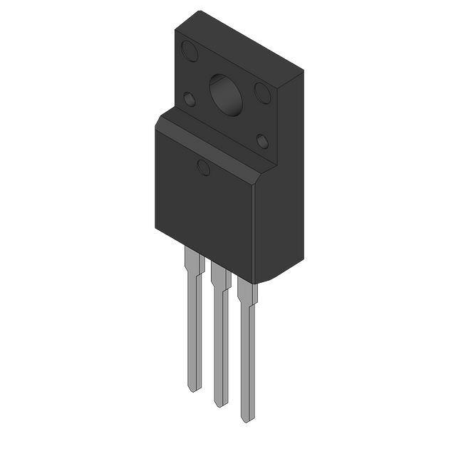
Package Dimensions
Low ON-resistance.
Ultrahigh-speed switching.
4V drive.
unit : mm
2063A
[2SJ650]
4.5
2.8
5.6
18.1
16.0
3.2
3.5
7.2
10.0
2.4
14.0
1.6
1.2
0.7
0.75
1 2 3
2.55
1 : Gate
2 : Drain
3 : Source
2.4
2.55
Specifications
2.55
Absolute Maximum Ratings at Ta=25°C
Parameter
Drain-to-Source Voltage
Gate-to-Source Voltage
Drain Current (DC)
Drain Current (Pulse)
Symbol
2.55
SANYO : TO-220ML
Conditions
Ratings
Unit
VDSS
VGSS
--60
±20
V
ID
--12
A
IDP
PW≤10µs, duty cycle≤1%
V
--48
A
2.0
W
Allowable Power Dissipation
PD
20
W
Channel Temperature
Tch
150
°C
Storage Temperature
Tstg
--55 to +150
°C
Tc=25°C
Electrical Characteristics at Ta=25°C
Parameter
Drain-to-Source Breakdown Voltage
Zero-Gate Voltage Drain Current
Gate-to-Source Leakage Current
Cutoff Voltage
Forward Transfer Admittance
Symbol
Conditions
V(BR)DSS
IDSS
IGSS
VGS(off)
yfs
typ
ID=--1mA, VGS=0
VDS=--60V, VGS=0
VGS=±16V, VDS=0
--60
VDS=--10V, ID=--1mA
--1.2
VDS=--10V, ID=--6A
Marking : J650
© 2011, SCILLC. All rights reserved.
Jan-2011, Rev. 0
Ratings
min
7
Unit
max
V
--1
µA
±10
µA
--2.6
10
V
S
Continued on next page.
www.onsemi.com
Rev.0 I Page
1 of 4 I www.onsemi.com
Publication Order Number:
2SJ650/D
�2SJ650
Continued from preceding page.
Ratings
Parameter
Symbol
Static Drain-to-Source On-State Resistance
RDS(on)1
RDS(on)2
ID=--6A, VGS=--10V
ID=--6A, VGS=--4V
100
135
mΩ
145
205
mΩ
Input Capacitance
Ciss
1020
Output Capacitance
Coss
VDS=--20V, f=1MHz
VDS=--20V, f=1MHz
Reverse Transfer Capacitance
Crss
Turn-ON Delay Time
td(on)
tr
Rise Time
Turn-OFF Delay Time
Conditions
td(off)
tf
Fall Time
Total Gate Charge
Qg
Gate-to-Source Charge
Qgs
min
typ
Unit
max
pF
110
pF
VDS=--20V, f=1MHz
See specified Test Circuit.
76
pF
10
ns
See specified Test Circuit.
145
ns
See specified Test Circuit.
85
ns
See specified Test Circuit.
96
ns
21
nC
3.8
nC
Gate-to-Drain“Miller”Charge
Qgd
VDS=--30V, VGS=--10V, ID=--12A
VDS=--30V, VGS=--10V, ID=--12A
VDS=--30V, VGS=--10V, ID=--12A
Diode Forward Voltage
VSD
IS=--12A, VGS=0
4.5
nC
--0.9
--1.2
V
Switching Time Test Circuit
VDD= --30V
VIN
0V
--10V
ID= --6A
RL=5Ω
VIN
D
VOUT
PW=10µs
D.C.≤1%
G
2SJ650
50Ω
Drain Current, ID -- A
--15
--4V
--10
--5
VGS= --3V
--0.5
--1.0
--1.5
--2.0
--2.5
--3.0
--3.5
--4.0
Drain-to-Source Voltage, VDS -- V
--4.5
--5.0
°C
--20
V
--6
75
V
--8
ID -- VGS
VDS= --10V
Tc=
--
--1
0V
Tc=25°C
--20
0
0
--25
25° 2
C 5°
C
ID -- VDS
--25
Drain Current, ID -- A
S
--15
--10
--5
0
0
25
°C
75
°C
Tc
=-25
°C
P.G
--0.5
IT06157
Rev.0 I Page 2 of 4 I www.onsemi.com
--1.0
--1.5
--2.0
--2.5
--3.0
--3.5
--4.0
Gate-to-Source Voltage, VGS -- V
--4.5
--5.0
IT06158
�2SJ650
RDS(on) -- VGS
Static Drain-to-Source
On-State Resistance, RDS(on) -- mΩ
250
200
75°C
150
25°C
100
Tc= --25°C
50
0
0
--1
--2
--3
--4
--5
--6
--7
--8
--9
Gate-to-Source Voltage, VGS -- V
Cutoff Voltage, VGS(off) -- V
--1.5
--1.0
--0.5
0
25
50
75
100
125
Case Temperature, Tc -- °C
0V
100
50
--25
0
25
50
75
100
VDS= --10V
7
5
3
2
C
25°
°C
--25
Tc=
75°C
10
7
5
3
2
1.0
7
5
2
3
5
7 --1.0
2
3
5
7 --10
VDD= --30V
VGS= --10V
7
3
2
td(off)
tf
100
7
5
tr
3
2
td(on)
10
0
--0.3
--0.6
--0.9
--1.2
7
5
--0.1
--1.5
Diode Forward Voltage, VSD -- V
Gate-to-Source Voltage, VGS -- V
3
Coss
100
7
5
Crss
3
2
7
2
--1.0
3
5
7
--10
IT06163
VDS= --30V
ID= --12A
--9
Ciss
5
VGS -- Qg
--10
f=1MHz
2
2
3
Drain Current, ID -- A
3
1000
7
5
2
IT06162
Ciss, Coss, Crss -- VDS
5
3
SW Time -- ID
1000
Switching Time, SW Time -- ns
--0.1
7
5
3
2
2
IT06161
5
--1.0
7
5
3
2
150
IT06160
Drain Current, ID -- A
VGS=0
--10
7
5
3
2
125
yfs -- ID
IT06169
Tc=
75°
C
25°C
--25°C
Forward Current, IF -- A
4V
= --1
, VGS
A
6
I D=
3
--0.1
150
--0.01
Ciss, Coss, Crss -- pF
= -V GS
,
--6A
Case Temperature, Tc -- °C
IF -- VSD
--100
7
5
3
2
I D=
150
100
--2.0
--25
200
IT06159
VDS= --10V
ID= --1mA
0
--50
250
0
--50
--10
VGS(off) -- Tc
--2.5
RDS(on) -- Tc
300
ID= --6A
Forward Transfer Admittance, yfs -- S
Static Drain-to-Source
On-State Resistance, RDS(on) -- mΩ
300
--8
--7
--6
--5
--4
--3
--2
--1
10
0
0
--5
--10
--15
--20
--25
Drain-to-Source Voltage, VDS -- V
--30
0
IT06164
Rev.0 I Page 3 of 4 I www.onsemi.com
5
10
15
Total Gate Charge, Qg -- nC
20
25
IT06165
�2SJ650
ASO
IDP= --48A
很抱歉,暂时无法提供与“2SJ650”相匹配的价格&库存,您可以联系我们找货
免费人工找货