3EZ6.2D5 Series
3 Watt DO-41 Surmetic
30 Zener Voltage Regulators
This is a complete series of 3 Watt Zener diodes with limits and
excellent operating characteristics that reflect the superior capabilities
of silicon−oxide passivated junctions. All this in an axial−lead,
transfer−molded plastic package that offers protection in all common
environmental conditions.
www.onsemi.com
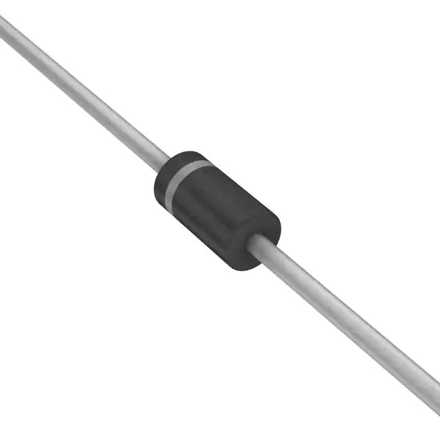
Cathode
Anode
Specification Features:
•
•
•
•
•
•
Zener Voltage Range − 6.2 V to 18 V
ESD Rating of Class 3 (>16 kV) per Human Body Model
Surge Rating of 98 W @ 1 ms
Maximum Limits Guaranteed on up to Six Electrical Parameters
Package No Larger than the Conventional 1 Watt Package
These are Pb−Free Devices*
Mechanical Characteristics:
CASE: Void free, transfer−molded, thermosetting plastic
FINISH: All external surfaces are corrosion resistant and leads are
AXIAL LEAD
CASE 59
PLASTIC
readily solderable
MAXIMUM LEAD TEMPERATURE FOR SOLDERING PURPOSES:
260°C, 1/16″ from the case for 10 seconds
POLARITY: Cathode indicated by polarity band
MOUNTING POSITION: Any
MARKING DIAGRAM
MAXIMUM RATINGS
Rating
Symbol
Value
Unit
Max. Steady State Power Dissipation
@ TL = 75°C, Lead Length = 3/8″
Derate above 75°C
PD
3
W
24
mW/°C
Steady State Power Dissipation
@ TA = 50°C
Derate above 50°C
PD
1
W
6.67
mW/°C
−65 to +200
°C
Operating and Storage Temperature
Range
TJ, Tstg
Stresses exceeding those listed in the Maximum Ratings table may damage the
device. If any of these limits are exceeded, device functionality should not be
assumed, damage may occur and reliability may be affected.
A
3EZ
xxD
YYWWG
G
A
= Assembly Location
3EZxxD = Device Number
YY
= Year
WW
= Work Week
G
= Pb−Free Package
(Note: Microdot may be in either location)
ORDERING INFORMATION
Package
Shipping†
3EZxxD5G
Axial Lead
(Pb−Free)
2000 Units / Box
3EZxxD5RLG
Axial Lead
(Pb−Free)
6000 / Tape & Reel
Device
*For additional information on our Pb−Free strategy and soldering details, please
download the ON Semiconductor Soldering and Mounting Techniques
Reference Manual, SOLDERRM/D.
© Semiconductor Components Industries, LLC, 2007
December, 2019 − Rev. 1
1
†For information on tape and reel specifications,
including part orientation and tape sizes, please
refer to our Tape and Reel Packaging Specifications
Brochure, BRD8011/D.
Publication Order Number:
3EZ6.2D5/D
�3EZ6.2D5 Series
ELECTRICAL CHARACTERISTICS (TA = 25°C unless
otherwise noted, VF = 1.5 V Max @ IF = 200 mA for all types)
Symbol
Parameter
I
VZ
Reverse Zener Voltage @ IZT
IZT
Reverse Current
ZZT
Maximum Zener Impedance @ IZT
IZK
Reverse Current
ZZK
Maximum Zener Impedance @ IZK
IF
IR
Reverse Leakage Current @ VR
VR
Breakdown Voltage
IF
Forward Current
VF
Forward Voltage @ IF
IZM
Maximum DC Zener Current
IR
Surge Current @ TA = 25°C
VZ VR
V
IR VF
IZT
Zener Voltage Regulator
ELECTRICAL CHARACTERISTICS (TA = 25°C unless otherwise noted, VF = 1.5 V Max @ IF = 200 mA for all types)
Zener Voltage (Note 2)
Device†
(Note 1)
Device
Marking
VZ (Volts)
Min
Nom
Max
Zener Impedance (Note 3)
@ IZT
ZZT @ IZT
mA
W
Leakage Current
ZZK @ IZK
W
mA
IR @ VR
mA Max
Volts
IZM
IR
(Note 4)
mA
mA
3EZ6.2D5RLG
3EZ6.2D
5.89
6.2
6.51
121
1.5
700
1
5
3
435
3.1
3EZ13D5G
3EZ13D
12.35
13
13.65
58
4.5
700
0.25
0.5
9.9
208
1.54
3EZ16D5RLG
3EZ16D
15.2
16
16.8
47
5.5
700
0.25
0.5
12.2
169
1.25
3EZ18D5RLG
3EZ18D
17.1
18
18.9
42
6.0
750
0.25
0.5
13.7
150
1.11
1. TOLERANCE AND TYPE NUMBER DESIGNATION
Tolerance designation − device tolerance of ±5% are indicated by a “5” suffix.
2. ZENER VOLTAGE (VZ) MEASUREMENT
ON Semiconductor guarantees the zener voltage when measured at 40 ms ±10 ms, 3/8″ from the diode body. And an ambient temperature
of 25°C (+8°C, −2°C)
3. ZENER IMPEDANCE (ZZ) DERIVATION
The zener impedance is derived from 60 seconds AC voltage, which results when an AC current having an rms value equal to 10% of the
DC zener current (IZT or IZK) is superimposed on IZT or IZK.
4. SURGE CURRENT (IR) NON−REPETITIVE
The rating listed in the electrical characteristics table is maximum peak, non−repetitive, reverse surge current of 1/2 square wave or
equivalent sine wave pulse of 1/120 second duration superimposed on the test current, IZT, per JEDEC standards. However, actual device
capability is as described in Figure 3 of the General Data sheet for Surmetic 30s.
†The “G’’ suffix indicates these are Pb−Free packages.
PD, STEADY STATE POWER
DISSIPATION (WATTS)
5
L = 1/8″
L = LEAD LENGTH
TO HEAT SINK
4
L = 3/8″
3
2
L = 1″
1
0
0
20
40
60
80 100 120 140 160
TL, LEAD TEMPERATURE (°C)
180
Figure 1. Power Temperature Derating Curve
www.onsemi.com
2
200
�3EZ6.2D5 Series
θJL(t, D) TRANSIENT THERMAL RESISTANCE
JUNCTION‐TO‐LEAD ( °C/W)
30
20
10
7
5
3
2
1
0.7
0.5
D =0.5
0.2
0.1
t2
DUTY CYCLE, D =t1/t2
0.02
0.01
NOTE: BELOW 0.1 SECOND, THERMAL
RESPONSE CURVE IS APPLICABLE
TO ANY LEAD LENGTH (L).
D=0
0.3
0.0001 0.0002
t1
PPK
0.05
0.0005
0.001
0.002
0.005
0.01
0.02
0.05
t, TIME (SECONDS)
0.1
0.2
SINGLE PULSE DTJL = qJL (t)PPK
REPETITIVE PULSES DTJL = qJL (t,D)PPK
0.5
1
2
5
10
PPK , PEAK SURGE POWER (WATTS)
1K
RECTANGULAR
NONREPETITIVE
WAVEFORM
TJ�=�25°C PRIOR
TO INITIAL PULSE
500
300
200
100
50
30
3
2
1
0.5
0.2 0.3 0.5
1
2 3
5
10
PW, PULSE WIDTH (ms)
20 30 50
100
TA = 125°C
0.2
0.1
0.05
0.02
0.01
0.005
0.002
0.001
0.0005
0.0003
20
10
0.1
IR , REVERSE LEAKAGE (μ Adc) @ VR
AS SPECIFIED IN ELEC. CHAR. TABLE
Figure 2. Typical Thermal Response L, Lead Length = 3/8 Inch
TA = 125°C
1
Figure 3. Maximum Surge Power
2
5
10
20
50 100
NOMINAL VZ (VOLTS)
200
400
1000
Figure 4. Typical Reverse Leakage
APPLICATION NOTE
DTJL is the increase in junction temperature above the lead
temperature and may be found from Figure 2 for a train of
power pulses (L = 3/8 inch) or from Figure 10 for dc power.
Since the actual voltage available from a given zener
diode is temperature dependent, it is necessary to determine
junction temperature under any set of operating conditions
in order to calculate its value. The following procedure is
recommended:
Lead Temperature, TL, should be determined from:
DTJL = qJL PD
For worst-case design, using expected limits of IZ, limits
of PD and the extremes of TJ (DTJ) may be estimated.
Changes in voltage, VZ, can then be found from:
TL = qLA PD + TA
qLA is the lead-to-ambient thermal resistance (°C/W) and
PD is the power dissipation. The value for qLA will vary and
depends on the device mounting method. qLA is generally
30−40°C/W for the various clips and tie points in common
use and for printed circuit board wiring.
The temperature of the lead can also be measured using a
thermocouple placed on the lead as close as possible to the
tie point. The thermal mass connected to the tie point is
normally large enough so that it will not significantly
respond to heat surges generated in the diode as a result of
pulsed operation once steady-state conditions are achieved.
Using the measured value of TL, the junction temperature
may be determined by:
DV = qVZ DTJ
qVZ, the zener voltage temperature coefficient, is found
from Figures 5 and 6.
Under high power-pulse operation, the zener voltage will
vary with time and may also be affected significantly by the
zener resistance. For best regulation, keep current
excursions as low as possible.
Data of Figure 2 should not be used to compute surge
capability. Surge limitations are given in Figure 3. They are
lower than would be expected by considering only junction
temperature, as current crowding effects cause temperatures
to be extremely high in small spots resulting in device
degradation should the limits of Figure 3 be exceeded.
TJ = TL + DTJL
www.onsemi.com
3
�3EZ6.2D5 Series
TEMPERATURE COEFFICIENT RANGES
10
8
6
4
RANGE
2
0
-2
-4
3
4
5
6
7
8
9
10
VZ, ZENER VOLTAGE @ IZT (VOLTS)
11
12
θ VZ, TEMPERATURE COEFFICIENT (mV/ °C) @ I ZT
θ VZ, TEMPERATURE COEFFICIENT (mV/ °C) @ I ZT
(90% of the Units are in the Ranges Indicated)
1000
500
200
100
50
20
10
10
20
50
100
200
400
VZ, ZENER VOLTAGE @ IZT (VOLTS)
Figure 5. Units to 12 Volts
1000
Figure 6. Units 10 to 400 Volts
ZENER VOLTAGE versus ZENER CURRENT
(Figures 7, 8 and 9)
50
30
20
IZ , ZENER CURRENT (mA)
100
50
30
20
IZ, ZENER CURRENT (mA)
100
10
5
3
2
1
0.5
0.3
0.2
0
1
2
3
4
5
6
7
VZ, ZENER VOLTAGE (VOLTS)
8
9
5
3
2
1
0.5
0.3
0.2
0.1
10
0
10
20
Figure 7. VZ = 3.3 thru 10 Volts
θJL, JUNCTION‐TO‐LEAD THERMAL RESISTANCE (° C/W)
0.1
10
30
40
50
60
70
VZ, ZENER VOLTAGE (VOLTS)
Figure 8. VZ = 12 thru 82 Volts
80
70
60
50
L
40
L
30
TL
20
PRIMARY PATH OF
CONDUCTION IS THROUGH
THE CATHODE LEAD
10
0
0
1/8
80
1/4
3/8
1/2
5/8
3/4
L, LEAD LENGTH TO HEAT SINK (INCH)
7/8
Figure 9. Typical Thermal Resistance
www.onsemi.com
4
1
90
100
�MECHANICAL CASE OUTLINE
PACKAGE DIMENSIONS
AXIAL LEAD
CASE 59−10
ISSUE U
DATE 15 FEB 2005
B
K
STYLE 1
NOTES:
1. DIMENSIONING AND TOLERANCING PER ANSI
Y14.5M, 1982.
2. CONTROLLING DIMENSION: INCH.
3. ALL RULES AND NOTES ASSOCIATED WITH
JEDEC DO−41 OUTLINE SHALL APPLY
4. POLARITY DENOTED BY CATHODE BAND.
5. LEAD DIAMETER NOT CONTROLLED WITHIN F
DIMENSION.
D
STYLE 2
F
A
SCALE 1:1
POLARITY INDICATOR
OPTIONAL AS NEEDED
(SEE STYLES)
F
K
DIM
A
B
D
F
K
INCHES
MIN
MAX
0.161 0.205
0.079 0.106
0.028 0.034
−−− 0.050
1.000
−−−
MILLIMETERS
MIN
MAX
4.10
5.20
2.00
2.70
0.71
0.86
−−−
1.27
25.40
−−−
GENERIC
MARKING DIAGRAM*
STYLE 1:
PIN 1. CATHODE (POLARITY BAND)
2. ANODE
STYLE 2:
NO POLARITY
A
xxx
xxx
YYWW
STYLE 1
xxx
A
YY
WW
A
xxx
xxx
YYWW
STYLE 2
= Specific Device Code
= Assembly Location
= Year
= Work Week
*This information is generic. Please refer to
device data sheet for actual part marking.
Pb−Free indicator, “G” or microdot “ G”,
may or may not be present.
DOCUMENT NUMBER:
DESCRIPTION:
98ASB42045B
AXIAL LEAD
Electronic versions are uncontrolled except when accessed directly from the Document Repository.
Printed versions are uncontrolled except when stamped “CONTROLLED COPY” in red.
PAGE 1 OF 1
ON Semiconductor and
are trademarks of Semiconductor Components Industries, LLC dba ON Semiconductor or its subsidiaries in the United States and/or other countries.
ON Semiconductor reserves the right to make changes without further notice to any products herein. ON Semiconductor makes no warranty, representation or guarantee regarding
the suitability of its products for any particular purpose, nor does ON Semiconductor assume any liability arising out of the application or use of any product or circuit, and specifically
disclaims any and all liability, including without limitation special, consequential or incidental damages. ON Semiconductor does not convey any license under its patent rights nor the
rights of others.
© Semiconductor Components Industries, LLC, 2019
www.onsemi.com
�onsemi,
, and other names, marks, and brands are registered and/or common law trademarks of Semiconductor Components Industries, LLC dba “onsemi” or its affiliates
and/or subsidiaries in the United States and/or other countries. onsemi owns the rights to a number of patents, trademarks, copyrights, trade secrets, and other intellectual property.
A listing of onsemi’s product/patent coverage may be accessed at www.onsemi.com/site/pdf/Patent−Marking.pdf. onsemi reserves the right to make changes at any time to any
products or information herein, without notice. The information herein is provided “as−is” and onsemi makes no warranty, representation or guarantee regarding the accuracy of the
information, product features, availability, functionality, or suitability of its products for any particular purpose, nor does onsemi assume any liability arising out of the application or use
of any product or circuit, and specifically disclaims any and all liability, including without limitation special, consequential or incidental damages. Buyer is responsible for its products
and applications using onsemi products, including compliance with all laws, regulations and safety requirements or standards, regardless of any support or applications information
provided by onsemi. “Typical” parameters which may be provided in onsemi data sheets and/or specifications can and do vary in different applications and actual performance may
vary over time. All operating parameters, including “Typicals” must be validated for each customer application by customer’s technical experts. onsemi does not convey any license
under any of its intellectual property rights nor the rights of others. onsemi products are not designed, intended, or authorized for use as a critical component in life support systems
or any FDA Class 3 medical devices or medical devices with a same or similar classification in a foreign jurisdiction or any devices intended for implantation in the human body. Should
Buyer purchase or use onsemi products for any such unintended or unauthorized application, Buyer shall indemnify and hold onsemi and its officers, employees, subsidiaries, affiliates,
and distributors harmless against all claims, costs, damages, and expenses, and reasonable attorney fees arising out of, directly or indirectly, any claim of personal injury or death
associated with such unintended or unauthorized use, even if such claim alleges that onsemi was negligent regarding the design or manufacture of the part. onsemi is an Equal
Opportunity/Affirmative Action Employer. This literature is subject to all applicable copyright laws and is not for resale in any manner.
PUBLICATION ORDERING INFORMATION
LITERATURE FULFILLMENT:
Email Requests to: orderlit@onsemi.com
onsemi Website: www.onsemi.com
◊
TECHNICAL SUPPORT
North American Technical Support:
Voice Mail: 1 800−282−9855 Toll Free USA/Canada
Phone: 011 421 33 790 2910
Europe, Middle East and Africa Technical Support:
Phone: 00421 33 790 2910
For additional information, please contact your local Sales Representative
�