Revised May 2005
74ACT16374
16-Bit D-Type Flip-Flop with 3-STATE Outputs
General Description
Features
The ACT16374 contains sixteen non-inverting D-type flipflops with 3-STATE outputs and is intended for bus oriented
applications. The device is byte controlled. A buffered clock
(CP) and Output Enable (OE) are common to each byte
and can be shorted together for full 16-bit operation.
■ Buffered Positive edge-triggered clock
■ Separate control logic for each byte
■ 16-bit version of the ACT374
■ Outputs source/sink 24 mA
■ TTL-compatible inputs
Ordering Code:
Order Number
Package Number
Package Description
74ACT16374SSC
MS48A
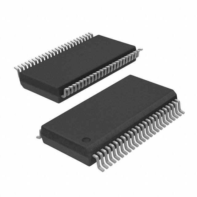
48-Lead Small Shrink Outline Package (SSOP), JEDEC MO-118, 0.300" Wide
74ACT16374MTD
MTD48
48-Lead Thin Shrink Small Outline Package (TSSOP), JEDEC MO-153, 6.1mm Wide
Device also available in Tape and Reel. Specify by appending suffix letter “X” to the ordering code.
Logic Symbol
Connection Diagram
Pin Descriptions
Pin Names
Description
OEn
Output Enable Input (Active LOW)
CPn
Clock Pulse Input
I0–I15
Inputs
O0–O15
Outputs
FACT¥ is a trademark of Fairchild Semiconductor Corporation.
© 2005 Fairchild Semiconductor Corporation
DS500298
www.fairchildsemi.com
74ACT16374 16-Bit D-Type Flip-Flop with 3-STATE Outputs
August 1999
�74ACT16374
Functional Description
Truth Tables
The ACT16374 consists of sixteen edge-triggered flip-flops
with individual D-type inputs and 3-STATE true outputs.
The device is byte controlled with each byte functioning
identically, but independent of the other. The control pins
can be shorted together to obtain full 16-bit operation. Each
byte has a buffered clock and buffered Output Enable common to all flip-flops within that byte. The description which
follows applies to each byte. Each flip-flop will store the
state of their individual D inputs that meet the setup and
hold time requirements on the LOW-to-HIGH Clock (CPn)
transition. With the Output Enable (OEn) LOW, the contents of the flip-flops are available at the outputs. When
OEn is HIGH, the outputs go to the high impedance state.
Operation of the OEn input does not affect the state of the
flip-flops.
Inputs
CP1
�
�
OE1
I0–I7
O0–O7
L
H
H
L
L
L
L
L
X
(Previous)
X
H
X
Z
Inputs
�
Logic Diagrams
Byte 1 (0:7)
Byte 2 (8:15)
2
Outputs
�
�
OE2
I8–I15
O8–O15
L
H
H
L
L
L
L
L
X
(Previous)
X
H
X
Z
CP2
H HIGH Voltage Level
L LOW Voltage Level
X Immaterial
Z HIGH Impedance
LOW-to-HIGH Transition
www.fairchildsemi.com
Outputs
�Recommended Operating
Conditions
�0.5V to �7.0V
Supply Voltage (VCC)
DC Input Diode Current (IIK)
VI
VI
�0.5V
VCC � 0.5V
Supply Voltage (VCC)
�20 mA
�20 mA
DC Output Diode Current (IOK)
VO
VO
�0.5V
VCC � 0.5V
DC Output Voltage (VO)
DC Output Source/Sink Current (IO)
per Output Pin
0V to VCC
Output Voltage (VO)
0V to VCC
�40qC to �85qC
Operating Temperature (TA)
�20 mA
�20 mA
�0.5V to VCC � 0.5V
r50 mA
Minimum Input Edge Rate ('V/'t)
125 mV/ns
VIN from 0.8V to 2.0V
VCC @ 4.5V, 5.5V
Note 1: Absolute maximum ratings are those values beyond which damage
to the device may occur. The databook specifications should be met, without exception to ensure that the system design is reliable over its power
supply, temperature, and output/input loading variables. Fairchild does not
recommend operation of FACT¥ circuits outside databook specifications.
DC VCC or Ground Current
Storage Temperature
4.5V to 5.5V
Input Voltage (VI)
r 50 mA
�65qC to �150qC
DC Electrical Characteristics
Symbol
VIH
VIL
VOH
VOL
IOZ
Parameter
VCC
TA
(V)
Typ
�25qC
TA
�40qC to �85qC
Guaranteed Limits
Minimum HIGH
4.5
1.5
2.0
2.0
Input Voltage
5.5
1.5
2.0
2.0
Maximum LOW
4.5
1.5
0.8
0.8
Input Voltage
5.5
1.5
0.8
0.8
Minimum HIGH
4.5
4.49
4.4
4.4
Output Voltage
5.5
5.49
5.4
5.4
4.5
3.86
3.76
5.5
4.86
4.76
Maximum LOW
4.5
0.001
0.1
0.1
Output Voltage
5.5
0.001
0.1
0.1
Maximum 3-STATE
Units
V
V
Maximum Input
VOUT
0.1V
or VCC � 0.1V
VOUT
0.1V
or VCC � 0.1V
V
IOUT
�50 PA
VIN
VIL or VIH
V
IOH
�24 mA
IOH
�24 mA (Note 2)
V
V
50 PA
IOUT
VIN
VIL or VIH
IOL
24 mA
4.5
0.36
0.44
5.5
0.36
0.44
5.5
r 0.5
r 5.0
PA
VI
5.5
r 0.1
r 1.0
PA
VI
VCC, GND
1.5
mA
VI
VCC � 2.1V
8.0
80.0
PA
VIN
75
mA
VOLD
1.65V Max
�75
mA
VOHD
3.85V Min
24 mA (Note 2)
IOL
Leakage Current
IIN
Conditions
VIL, VIH
VO
VCC, GND
Leakage Current
ICCT
Maximum ICC/Input
5.5
ICC
Maximum Quiescent
5.5
0.6
VCC or GND
Supply Current
IOLD
Minimum Dynamic
IOHD
Output Current (Note 3)
5.5
Note 2: All outputs loaded; thresholds associated with output under test.
Note 3: Maximum test duration 2.0 ms; one output loaded at a time.
3
www.fairchildsemi.com
74ACT16374
Absolute Maximum Ratings(Note 1)
�74ACT16374
AC Electrical Characteristics
Symbol
Parameter
VCC
TA
�25qC
(V)
CL
50 pF
(Note 4)
fMAX
Maximum Clock Frequency
tPLH
Propagation Delay
tPHL
CP to On
tPZH
Output Enable Time
5.0
5.0
Output Disable Time
5.0
tPLZ
�40qC to �85qC
CL
50 pF
Typ
Max
Min
3.1
5.3
7.9
3.1
8.4
3.0
5.1
7.3
3.0
7.8
2.5
4.7
7.4
2.5
7.9
3.0
5.4
8.0
2.0
8.5
2.1
5.1
7.9
2.1
8.2
2.0
4.8
7.4
2.0
7.9
71
5.0
tPZL
tPHZ
Min
TA
Units
Max
67
MHz
ns
ns
ns
Note 4: Voltage Range 5.0 is 5.0V r 0.5V.
AC Operating Requirements
Symbol
tS
Parameter
Setup Time, HIGH or
LOW, Input to Clock
tH
Hold Time, HIGH or
LOW, Input to Clock
tW
CP Pulse Width,
HIGH or LOW
VCC
TA
�25qC
(V)
CL
50 pF
TA
�40qC to �85qC
CL
50 pF
Typ
Guaranteed Limits
5.0
0.7
3.0
3.0
ns
5.0
0.8
1.0
1.0
ns
5.0
1.5
5.0
5.0
ns
Note 5: Voltage Range 5.0 is 5.0V r 0.5V.
Capacitance
Symbol
Parameter
Typ
Units
CIN
Input Capacitance
4.5
pF
VCC
5.0V
CPD
Power Dissipation Capacitance
30
pF
VCC
5.0V
www.fairchildsemi.com
Units
(Note 5)
4
Conditions
�74ACT16374
Physical Dimensions inches (millimeters) unless otherwise noted
48-Lead Small Shrink Outline Package (SSOP), JEDEC MO-118, 0.300" Wide
Package Number MS48A
5
www.fairchildsemi.com
�74ACT16374 16-Bit D-Type Flip-Flop with 3-STATE Outputs
Physical Dimensions inches (millimeters) unless otherwise noted (Continued)
48-Lead Thin Shrink Small Outline Package (TSSOP), JEDEC MO-153, 6.1mm Wide
Package Number MTD48
Fairchild does not assume any responsibility for use of any circuitry described, no circuit patent licenses are implied and
Fairchild reserves the right at any time without notice to change said circuitry and specifications.
LIFE SUPPORT POLICY
FAIRCHILD’S PRODUCTS ARE NOT AUTHORIZED FOR USE AS CRITICAL COMPONENTS IN LIFE SUPPORT
DEVICES OR SYSTEMS WITHOUT THE EXPRESS WRITTEN APPROVAL OF THE PRESIDENT OF FAIRCHILD
SEMICONDUCTOR CORPORATION. As used herein:
2. A critical component in any component of a life support
device or system whose failure to perform can be reasonably expected to cause the failure of the life support
device or system, or to affect its safety or effectiveness.
1. Life support devices or systems are devices or systems
which, (a) are intended for surgical implant into the
body, or (b) support or sustain life, and (c) whose failure
to perform when properly used in accordance with
instructions for use provided in the labeling, can be reasonably expected to result in a significant injury to the
user.
www.fairchildsemi.com
www.fairchildsemi.com
6
�
很抱歉,暂时无法提供与“74ACT16374MTDX”相匹配的价格&库存,您可以联系我们找货
免费人工找货- 国内价格 香港价格
- 1000+9.080181000+1.18040
- 2000+8.434182000+1.09642
- 3000+8.399943000+1.09197