Revised October 2001
74ALVC162374
Low Voltage 16-Bit D-Type Flip-Flop
with 3.6V Tolerant Inputs and Outputs
and 26Ω Series Resistors in Outputs
General Description
Features
The ALVC162374 contains sixteen non-inverting D-type
flip-flops with 3-STATE outputs and is intended for bus oriented applications. The device is byte controlled. A buffered clock (CP) and output enable (OE) are common to
each byte and can be shorted together for full 16-bit operation.
■ 1.65V–3.6V VCC supply operation
The ALVC162374 is also designed with 26Ω series resistors in the outputs. This design reduces line noise in applications such as memory address drivers, clock drivers and
bus transceivers/transmitters.
■ 3.6V tolerant inputs and outputs
■ 26Ω series resistors in outputs
■ tPD (CLK to O n)
3.9 ns max for 3.0V to 3.6V VCC
5.3 ns max for 2.3V to 2.7V VCC
9.6 ns max for 1.65V to 1.95V VCC
■ Power-off high impedance inputs and outputs
The 74ALVC162374 is designed for low voltage (1.65V to
3.6V) VCC applications with I/O compatibility up to 3.6V.
■ Supports live insertion and withdrawal (Note 1)
The 74ALVC162374 is fabricated with an advanced CMOS
technology to achieve high speed operation while maintaining low CMOS power dissipation.
■ Latchup conforms to JEDEC JED78
■ Uses patented noise/EMI reduction circuitry
■ ESD performance:
Human body model > 2000V
Machine model > 200V
Note 1: To ensure the high-impedance state during power up or power
down, OE should be tied to VCC through a pull-up resistor; the minimum
value of the resistor is determined by the current-sourcing capability of the
driver.
Ordering Code:
Order Number
Package Number
Package Descriptions
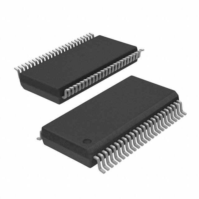
MTD48
48-Lead Thin Shrink Small Outline Package (TSSOP), JEDEC MO-153, 6.1mm Wide
74ALVC162374T
Devices also available in Tape and Reel. Specify by appending suffix letter “X” to the ordering code.
Logic Symbol
Pin Descriptions
Pin Names
© 2001 Fairchild Semiconductor Corporation
DS500688
Description
OEn
Output Enable Input (Active LOW)
CPn
Clock Pulse Input
I0–I15
Inputs
O0–O15
Outputs
www.fairchildsemi.com
74ALVC162374 Low Voltage 16-Bit D-Type Flip-Flop
October 2001
�74ALVC162374
Connection Diagram
Truth Tables
Inputs
CP1
�
�
Outputs
OE1
I0–I7
O0–O7
L
H
H
L
L
L
L
L
X
O0
X
H
X
Z
Inputs
CP2
Outputs
�
�
OE2
I8–I15
O8–O15
L
H
H
L
L
L
L
L
X
O0
X
H
X
Z
H = HIGH Voltage Level
L = LOW Voltage Level
X = Immaterial (HIGH or LOW, inputs may not float)
Z = High Impedance
O0 = Previous O0 before HIGH-to-LOW of CP
Functional Description
flop will store the state of their individual I inputs that meet
the setup and hold time requirements on the LOW-to-HIGH
Clock (CPn) transition. With the Output Enable (OEn) LOW,
the contents of the flip-flops are available at the outputs.
When OEn is HIGH, the outputs go to the high impedance
state. Operations of the OEn input does not affect the state
of the flip-flops.
The 74ALVC162374 consists of sixteen edge-triggered flipflops with individual D-type inputs and 3-STATE true outputs. The device is byte controlled with each byte functioning identically, but independent of the other. The control
pins can be shorted together to obtain full 16-bit operation.
Each clock has a buffered clock and buffered Output
Enable common to all flip-flops within that byte. The
description which follows applies to each byte. Each flip-
Logic Diagram
Byte 1 (0:7)
Byte 2 (8:15)
Please note that this diagram is provided only for the understanding of logic operations and should not be used to estimate propagation delays.
www.fairchildsemi.com
2
�Recommended Operating
Conditions (Note 4)
−0.5V to +4.6V
Supply Voltage (VCC)
−0.5V to 4.6V
DC Input Voltage (VI)
Output Voltage (VO) (Note 3)
Power Supply
−0.5V to VCC +0.5V
Operating
DC Input Diode Current (IIK)
VI < 0V
−50 mA
0V to VCC
Output Voltage (VO)
DC Output Diode Current (IOK)
0V to VCC
Free Air Operating Temperature (TA)
VO < 0V
−50 mA
−40°C to +85°C
Minimum Input Edge Rate (∆t/∆V)
VIN = 0.8V to 2.0V, VCC = 3.0V
DC Output Source/Sink Current
±50 mA
(IOH/IOL)
±100 mA
Supply Pin (ICC or GND)
10 ns/V
Note 2: The Absolute Maximum Ratings are those values beyond which
the safety of the device cannot be guaranteed. The device should not be
operated at these limits. The parametric values defined in the Electrical
Characteristics tables are not guaranteed at the Absolute Maximum Ratings. The “Recommended Operating Conditions” table will define the conditions for actual device operation.
DC VCC or GND Current per
Storage Temperature Range (TSTG)
1.65V to 3.6V
Input Voltage
−65°C to +150°C
Note 3: IO Absolute Maximum Rating must be observed.
Note 4: Floating or unused control inputs must be held HIGH or LOW.
DC Electrical Characteristics
Symbol
VIH
VIL
VOH
VOL
Parameter
Conditions
HIGH Level Input Voltage
LOW Level Input Voltage
HIGH Level Output Voltage
LOW Level Output Voltage
IOH = −100 µA
VCC
(V)
Min
1.65 - 1.95
0.65 x VCC
2.3 - 2.7
1.7
2.7 - 3.6
2.0
Max
V
1.65 - 1.95
0.35 x VCC
2.3 - 2.7
0.7
2.7 - 3.6
0.8
1.65 - 3.6
Units
V
VCC - 0.2
IOH = −2 mA
1.65
1.2
IOH = −4 mA
2.3
1.9
IOH = −6 mA
2.3
1.7
3
2.4
IOH = −8 mA
2.7
2
IOH = −12 mA
3.0
2
IOL = 100 µA
1.65 - 3.6
0.2
IOL = 2 mA
1.65
0.45
IOL = 4 mA
2.3
0.4
IOL = 6 mA
2.3
0.55
3
0.55
V
IOL = 8 mA
2.7
0.6
IOL = 12 mA
3
0.8
V
II
Input Leakage Current
0 ≤ VI ≤ 3.6V
3.6
±5.0
µA
IOZ
3-STATE Output Leakage
0 ≤ VO ≤ 3.6V
3.6
±10
µA
ICC
Quiescent Supply Current
VI = V CC or GND, IO = 0
3.6
40
µA
∆ICC
Increase in ICC per Input
VIH = VCC − 0.6V
3 - 3.6
750
µA
3
www.fairchildsemi.com
74ALVC162374
Absolute Maximum Ratings(Note 2)
�74ALVC162374
AC Electrical Characteristics
TA = −40°C to +85°C, RL = 500Ω
Symbol
CL = 50 pF
Parameter
VCC = 3.3V ± 0.3V
Min
fMAX
Maximum Clock Frequency
tPHL, tPL
Propagation Delay
Max
250
CL = 30 pF
VCC = 2.7V
Min
Max
200
VCC = 2.5V ± 0.2V
Min
VCC = 1.8V ± 0.15V
Max
Min
200
Units
Max
100
ns
1.3
3.9
1.5
5.3
1.0
4.8
1.5
9.6
ns
1.3
4.4
1.5
5.9
1.0
5.4
1.5
9.8
ns
Output Disable Time
1.3
4.5
1.5
4.9
1.0
4.4
1.5
7.9
ns
Pulse Width
1.5
1.5
1.5
4.0
tS
Setup Time
1.5
1.5
1.5
2.5
ns
tH
Hold Time
1.0
1.0
1.0
1.0
ns
Bus to Bus
tPZL, tPZH
Output Enable Time
tPLZ, tPHZ
tW
ns
Capacitance
Symbol
Parameter
Conditions
TA = +25°C
Units
VCC
Typical
CIN
Input Capacitance
VI = 0V or VCC
3.3
6
pF
COUT
Output Capacitance
VI = 0V or VCC
3.3
7
pF
CPD
Power Dissipation Capacitance
3.3
20
2.5
20
www.fairchildsemi.com
Outputs Enabled f = 10 MHz, CL = 50 pF
4
pF
�TABLE 1. Values for Figure 1
TEST
SWITCH
tPLH, tPHL
Open
tPZL, tPLZ
VL
tPZH, tPHZ
GND
FIGURE 1. AC Test Circuit
TABLE 2. Variable Matrix
(Input Characteristics: f = 1MHz; tr = tf = 2ns; Z0 = 50Ω)
Symbol
VCC
3.3V ± 0.3V
2.7V
2.5V ± 0.2V
1.8V ± 0.15V
Vmi
1.5V
1.5V
VCC/2
VCC /2
Vmo
1.5V
1.5V
VCC/2
VCC /2
VX
VOL + 0.3V
VOL + 0.3V
VOL + 0.15V
VOL + 0.15V
VY
VOH − 0.3V
VOH − 0.3V
VOH − 0.15V
VOH − 0.15V
VL
6V
6V
VCC*2
VCC*2
FIGURE 3. 3-STATE Output High Enable and
Disable Times for Low Voltage Logic
FIGURE 2. Waveform for Inverting and
Non-Inverting Functions
FIGURE 4. 3-STATE Output Low Enable and Disable Times for Low Voltage Logic
FIGURE 6. Setup Time, Hold Time and
Recovery Time for Low Voltage Logic
FIGURE 5. Propagation Delay, Pulse Width and
tREC Waveforms
5
www.fairchildsemi.com
74ALVC162374
AC Loading and Waveforms
�74ALVC162374 Low Voltage 16-Bit D-Type Flip-Flop
Physical Dimensions inches (millimeters) unless otherwise noted
48-Lead Thin Shrink Small Outline Package (TSSOP), JEDEC MO-153, 6.1mm Body Width
Package Number MTD48
Fairchild does not assume any responsibility for use of any circuitry described, no circuit patent licenses are implied and
Fairchild reserves the right at any time without notice to change said circuitry and specifications.
LIFE SUPPORT POLICY
FAIRCHILD’S PRODUCTS ARE NOT AUTHORIZED FOR USE AS CRITICAL COMPONENTS IN LIFE SUPPORT
DEVICES OR SYSTEMS WITHOUT THE EXPRESS WRITTEN APPROVAL OF THE PRESIDENT OF FAIRCHILD
SEMICONDUCTOR CORPORATION. As used herein:
2. A critical component in any component of a life support
device or system whose failure to perform can be reasonably expected to cause the failure of the life support
device or system, or to affect its safety or effectiveness.
1. Life support devices or systems are devices or systems
which, (a) are intended for surgical implant into the
body, or (b) support or sustain life, and (c) whose failure
to perform when properly used in accordance with
instructions for use provided in the labeling, can be reasonably expected to result in a significant injury to the
user.
www.fairchildsemi.com
www.fairchildsemi.com
6
�
很抱歉,暂时无法提供与“74ALVC162374TX”相匹配的价格&库存,您可以联系我们找货
免费人工找货