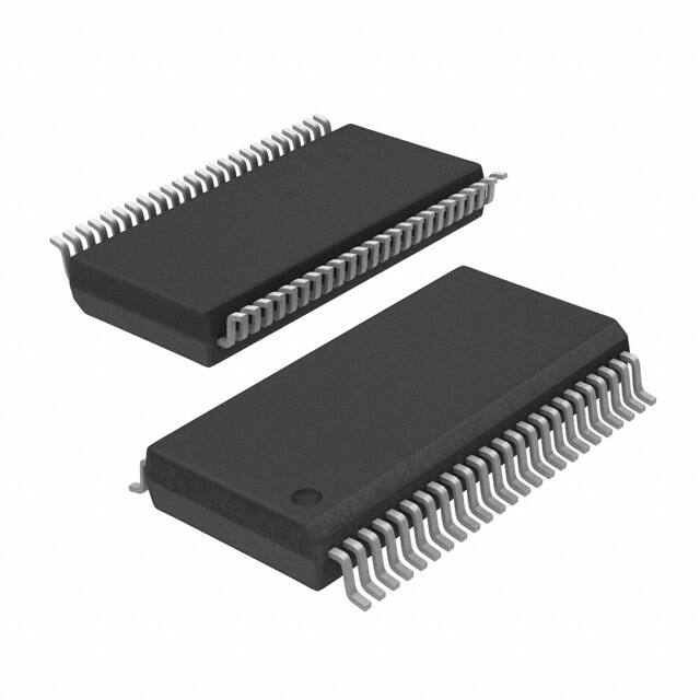
74ALVCH16244
Low−Voltage 16−Bit Buffer
with Bus Hold 1.8/2.5/3.3 V
(3−State, Non−Inverting)
The 74ALVCH16244 is an advanced performance, non−inverting
16−bit buffer. It is designed for very high−speed, very low−power
operation in 1.8 V, 2.5 V or 3.3 V systems.
The 74ALVCH16244 is nibble controlled with each nibble
functioning identically, but independently. The control pins may be
tied together to obtain full 16−bit operation. The 3−state outputs are
controlled by an Output Enable (OEn) input for each nibble. When
OEn is LOW, the outputs are on. When OEn is HIGH, the outputs are
in the high impedance state. The data inputs include active bushold
circuitry, eliminating the need for external pull−up resistors to hold
unused or floating inputs at a valid logic state.
• Designed for Low Voltage Operation: VCC = 1.65 − 3.6 V
• 3.6 V Tolerant Inputs and Outputs
• High Speed Operation: 3.0 ns max for 3.0 to 3.6 V
•
•
•
•
•
•
•
•
http://onsemi.com
MARKING DIAGRAM
48
48
74ALVCH16244DT
1
AWLYYWW
TSSOP−48
DT SUFFIX
CASE 1201
A
1
= Assembly
3.7 ns max for 2.3 to 2.7 V
Location
6.0 ns max for 1.65 to 1.95 V
WL
= Wafer Lot
YY
= Year
Static Drive:
±24 mA Drive at 3.0 V
WW
= Work Week
±12 mA Drive at 2.3 V
±4 mA Drive at 1.65 V
Supports Live Insertion and Withdrawal
Includes Active Bushold to Hold Unused or Floating Inputs at a Valid ORDERING INFORMATION
Logic State
Device
Package
Shipping
IOFF Specification Guarantees High Impedance When VCC = 0 V†
74ALVCH16244DTR TSSOP 2500/Tape & Reel
Near Zero Static Supply Current in All Three Logic States (40 mA)
Substantially Reduces System Power Requirements
Latchup Performance Exceeds ±250 mA @ 125°C
ESD Performance: Human Body Model >2000V; Machine Model >200V
Second Source to Industry Standard 74ALVCH16244
†To ensure the outputs activate in the 3−state condition, the output enable pins
should be connected to VCC through a pull−up resistor. The value of the resistor is
determined by the current sinking capability of the output connected to the OE pin.
© Semiconductor Components Industries, LLC, 2006
June, 2006 − Rev. 2
1
Publication Order Number:
74ALVCH16244/D
�74ALVCH16244
OE1 1
48 OE2
O0 2
47 D0
O1 3
46 D1
GND 4
1
OE1
OE3
48
OE2
OE4
25
24
45 GND
O2 5
44 D2
O3 6
43 D3
VCC 7
42 VCC
O4 8
41 D4
O5 9
40 D5
GND 10
D0:3
O0:3
D8:11
O8:11
D4:7
O4:7
D12:15
O12:15
One of Four
39 GND
O6 11
38 D6
O7 12
37 D7
O8 13
36 D8
O9 14
35 D9
GND 15
34 GND
O10 16
33 D10
O11 17
32 D11
VCC 18
31 VCC
O12 19
30 D12
O13 20
29 D13
GND 21
28 GND
O14 22
27 D14
O15 23
26 D15
OE4 24
25 OE3
Figure 2. Logic Diagram
1
OE1
48
OE2
25
OE3
24
OE4
D0
D1
D2
D3
D4
D5
D6
D7
D8
D9
D10
D11
D12
D13
D14
D15
Figure 1. 48−Lead Pinout
(Top View)
PIN NAMES
Pins
Function
OEn
D0−D15
O0−O15
Output Enable Inputs
Inputs
Outputs
EN1
EN2
EN3
EN4
47
1
46
1∇
2
3
5
44
43
41
1
2∇
6
8
40
9
38
11
37
36
1
3∇
12
13
35
14
33
16
32
30
1
4∇
17
19
29
20
27
22
26
23
O0
O1
O2
O3
O4
O5
O6
O7
O8
O9
O10
O11
O12
O13
O14
O15
Figure 3. IEC Logic Diagram
OE1
D0:3
O0:3
OE2
D4:7
O4:7
OE3
D8:11
O8:11
OE4
D12:15
O12:15
L
L
L
L
L
L
L
L
L
L
L
L
L
H
H
L
H
H
L
H
H
L
H
H
H
X
Z
H
X
Z
H
X
Z
H
X
Z
H = High Voltage Level; L = Low Voltage Level; Z = High Impedance State; X = High or Low Voltage Level and Transitions Are Acceptable, for
ICC reasons, DO NOT FLOAT Inputs
http://onsemi.com
2
�74ALVCH16244
MAXIMUM RATINGS (Note 1)
Symbol
Parameter
Value
Unit
VCC
DC Supply Voltage
�0.5 to �4.6
V
VI
DC Input Voltage
�0.5 to �4.6
V
VO
DC Output Voltage
�0.5 to �4.6
V
IIK
DC Input Diode Current
VI < GND
�50
mA
IOK
DC Output Diode Current
VO < GND
�50
mA
IO
DC Output Sink Current
�50
mA
ICC
DC Supply Current per Supply Pin
�100
mA
IGND
DC Ground Current per Ground Pin
�100
mA
TSTG
Storage Temperature Range
�65 to �150
°C
TL
Lead Temperature, 1 mm from Case for 10 Seconds
TJ
Junction Temperature Under Bias
qJA
Thermal Resistance (Note 2)
MSL
Moisture Sensitivity
FR
Flammability Rating
VESD
ESD Withstand Voltage
Human Body Model (Note 3)
Machine Model (Note 4)
Charged Device Model (Note 5)
�2000
�200
N/A
V
ILATCH−UP
Latch−Up Performance
Above VCC and Below GND at 125°C (Note 6)
�250
mA
260
°C
�150
°C
90
°C/W
Level 1
Oxygen Index: 30 to 35
UL 94 V−O @ 0.125 in
Stresses exceeding Maximum Ratings may damage the device. Maximum Ratings are stress ratings only. Functional operation above the
Recommended Operating Conditions is not implied. Extended exposure to stresses above the Recommended Operating Conditions may affect
device reliability.
1. IO absolute maximum rating must be observed.
2. Measured with minimum pad spacing on an FR4 board, using 10 mm−by−1 inch, 2−ounce copper trace with no air flow.
3. Tested to EIA/JESD22−A114−A.
4. Tested to EIA/JESD22−A115−A.
5. Tested to JESD22−C101−A.
6. Tested to EIA/JESD78.
RECOMMENDED OPERATING CONDITIONS
Symbol
Parameter
VCC
Supply Voltage
VI
Input Voltage
VO
Output Voltage
TA
Operating Free−Air Temperature
Dt/DV
Input Transition Rise or Fall Rate
Min
Max
Unit
Operating
Data Retention Only
2.3
1.5
3.6
3.6
V
(Note 7)
−0.5
3.6
V
0
0
3.6
3.6
V
�40
�85
°C
0
0
20
10
ns/V
(Active State)
(3−State)
VCC = 2.5 V �
VCC = 3.0 V �
0.2 V
0.3 V
7. Unused inputs may not be left open. All inputs must be tied to a high−logic voltage level or a low−logic input voltage level.
http://onsemi.com
3
�74ALVCH16244
DC ELECTRICAL CHARACTERISTICS
TA = *405C to )855C
Symbol
VIH
VIL
VOH
VOL
Parameter
HIGH Level Input Voltage
(Note 8)
LOW Level Input Voltage
(Note 8)
HIGH Level Output Voltage
LOW Level Output Voltage
Condition
Min
1.65 V � VCC � 2.3 V
0.65 � VCC
2.3 V � VCC � 2.7 V
1.7
2.7 V � VCC � 3.6 V
2.0
Max
V
1.65 V � VCC � 2.3 V
0.35 � VCC
2.3 V � VCC � 2.7 V
0.7
2.7 V � VCC � 3.6 V
0.8
1.65 V � VCC � 3.6 V; IOH = �100 mA
1.20
VCC = 2.3 V; IOH = �6 mA
2.0
VCC = 2.3 V; IOH = �12 mA
1.7
VCC = 2.7 V; IOH = �12 mA
2.2
VCC = 3.0 V; IOH = �12 mA
2.4
VCC = 3.0 V; IOH = �24 mA
2.0
V
V
VCC � 0.2
VCC = 1.65 V; IOH = �4 mA
Unit
1.65 V � VCC � 3.6 V; IOL = 100 mA
0.2
VCC = 1.65 V; IOL = 4 mA
0.45
VCC = 2.3 V; IOL = 6 mA
0.4
VCC = 2.3 V; IOL = 12 mA
0.7
VCC = 2.7 V; IOL = 12 mA
0.4
VCC = 3.0 V; IOL = 24 mA
0.55
V
II
Input Leakage Current
1.65 V � VCC � 3.6 V; 0 V � VI � 3.6 V
�5.0
mA
II(HOLD)
Minimum Bus−hold Input
Current
VCC = 3.6 V; VIN = 0 to 3.6 V
�500
mA
VCC = 3.0 V, VIN = 0.8 V
75
VCC = 3.0 V, VIN = 2.0 V
�75
VCC = 2.3 V, VIN = 0.7 V
45
VCC = 2.3 V, VIN = 1.7 V
�45
VCC = 1.65 V, VIN = 0.58 V
25
VCC = 1.65 V, VIN = 1.07 V
�25
IOZ
3−State Output Current
1.65 V � VCC � 3.6 V; 0 V � VO � 3.6 V; VI = VIH or VIL
�10
mA
IOFF
Power−Off Leakage Current
VCC = 0 V; VI or VO = 3.6 V
10
mA
ICC
Quiescent Supply Current
(Note 9)
1.65 V � VCC � 3.6 V; VI = GND or VCC
40
mA
1.65 V � VCC � 3.6 V; 3.6 V � VI, VO � 3.6 V
�40
Increase in ICC per Input
2.7 V � VCC ≤ 3.6 V; VIH = VCC � 0.6 V
750
DICC
8. These values of VI are used to test DC electrical characteristics only.
9. Outputs disabled or 3−state only.
http://onsemi.com
4
mA
�74ALVCH16244
AC CHARACTERISTICS (Note 10; tR = tF = 2.0 ns; CL = 30 pF; RL = 500 W)
Limits
TA = −40°C to +85°C
VCC = 3.0 V to 3.6 V
VCC = 2.3 V to 2.7 V
VCC = 1.65 V − 1.95 V
Waveform
Min
Max
Min
Max
Min
Max
Unit
tPLH
tPHL
Propagation Delay
Input to Output
1
1.0
1.0
3.0
3.0
1.0
1.0
3.7
3.7
1.0
1.0
6.0
6.0
ns
tPZH
tPZL
Output Enable Time to
High and Low Level
2
1.0
1.0
4.4
4.4
1.0
1.0
5.7
5.7
1.0
1.0
8.2
8.2
ns
tPHZ
tPLZ
Output Disable Time From
High and Low Level
2
1.0
1.0
4.1
4.1
1.0
1.0
5.2
5.2
1.0
1.0
6.8
6.8
ns
tOSHL
tOSLH
Output−to−Output Skew
(Note 11)
0.75
0.75
ns
Symbol
Parameter
0.5
0.5
0.5
0.5
10. For CL = 50 pF, add approximately 300 ps to the AC maximum specification.
11. Skew is defined as the absolute value of the difference between the actual propagation delay for any two separate outputs of the same device.
The specification applies to any outputs switching in the same direction, either HIGH−to−LOW (tOSHL) or LOW−to−HIGH (tOSLH); parameter
guaranteed by design.
CAPACITIVE CHARACTERISTICS
Symbol
Parameter
Condition
Typical
Unit
CIN
Input Capacitance
Note 12
6
pF
COUT
Output Capacitance
Note 12
7
pF
CPD
Power Dissipation Capacitance
Note 12, 10 MHz
20
pF
12. VCC = 1.8, 2.5 or 3.3 V; VI = 0 4 V or VCC.
VIH
Dn
Vm
Vm
0V
tPLH
tPHL
On
Vm
VOH
Vm
VOL
WAVEFORM 1 − PROPAGATION DELAYS
tR = tF = 2.0 ns, 10% to 90%; f = 1 MHz; tW = 500 ns
VIH
OEn
Vm
0V
tPZH
On
tPHZ
Vm
VOH
Vy
≈0V
tPZL
On
tPLZ
≈ VCC
Vm
Vx
VOL
WAVEFORM 2 − OUTPUT ENABLE AND DISABLE TIMES
tR = tF = 2.0 ns, 10% to 90%; f = 1 MHz; tW = 500 ns
Figure 4. AC Waveforms
http://onsemi.com
5
�74ALVCH16244
VCC
Symbol
3.3 V ±0.3 V
2.5 V ±0.2 V
1.8 V ±0.15 V
VIH
2.7 V
VCC
VCC
Vm
1.5 V
VCC/2
VCC/2
Vx
VOL + 0.3 V
VOL + 0.15 V
VOL + 0.15 V
Vy
VOH − 0.3 V
VOH − 0.15 V
VOH − 0.15 V
VCC
PULSE
GENERATOR
RL
DUT
RT
CL
TEST
RL
SWITCH
tPLH, tPHL
Open
tPZL, tPLZ
6 V at VCC = 3.3 ±0.3 V;
VCC × 2 at VCC = 2.5 ±0.2 V; 1.8 ±0.15 V
tPZH, tPHZ
GND
CL = 50 pF for VCC = 3.0 ± 0.3 V
RL = 500 W or equivalent
RT = ZOUT of pulse generator (typically 50 W)
Figure 5. Test Circuit
http://onsemi.com
6
6V or VCC × 2
OPEN
GND
�74ALVCH16244
10 PITCHES
CUMULATIVE
TOLERANCE ON
TAPE
±0.2 mm
(±0.008")
P0
K
P2
D
t
TOP
COVER
TAPE
E
A0
+
K0
SEE
NOTE 2
B1
SEE NOTE 2
F
+
B0
W
+
P
EMBOSSMENT
FOR MACHINE REFERENCE
ONLY
INCLUDING DRAFT AND RADII
CONCENTRIC AROUND B0
CENTER LINES
OF CAVITY
D1
FOR COMPONENTS
2.0 mm × 1.2 mm
AND LARGER
USER DIRECTION OF FEED
*TOP COVER
TAPE THICKNESS (t1)
0.10 mm
(0.004") MAX
R MIN
BENDING RADIUS
10°
TAPE AND COMPONENTS
SHALL PASS AROUND RADIUS �R"
WITHOUT DAMAGE
EMBOSSED
CARRIER
100 mm
(3.937")
MAXIMUM COMPONENT ROTATION
EMBOSSMENT
1 mm MAX
TYPICAL
COMPONENT CAVITY
CENTER LINE
TAPE
1 mm
(0.039") MAX
TYPICAL
COMPONENT
CENTER LINE
250 mm
(9.843")
CAMBER (TOP VIEW)
ALLOWABLE CAMBER TO BE 1 mm/100 mm NONACCUMULATIVE OVER 250 mm
Figure 6. Carrier Tape Specifications
EMBOSSED CARRIER DIMENSIONS (See Notes 13 and 14)
Tape
Size
B1
Max
24mm
20.1mm
(0.791")
D
D1
E
F
K
P
P0
P2
R
T
W
1.5 + 0.1mm
1.5mm
1.75
11.5
11.9 mm
16.0
4.0
2.0
30 mm
0.6 mm
24.3 mm
−0.0
Min
±0.1 mm ±0.10 mm
Max
±0.1 mm
±0.1 mm
±0.1 mm
(1.18")
(0.024")
(0.957")
(0.059
(0.060")
(0.069
(0.453
(0.468")
(0.63
(0.157
(0.079
+0.004" −0.0)
±0.004")
±0.004")
±0.004")
±0.004")
±0.004")
13. Metric Dimensions Govern−English are in parentheses for reference only.
14. A0, B0, and K0 are determined by component size. The clearance between the components and the cavity must be within 0.05 mm min to
0.50 mm max. The component cannot rotate more than 10° within the determined cavity.
http://onsemi.com
7
�74ALVCH16244
t MAX
13.0 mm ±0.2 mm
(0.512" ±0.008")
1.5 mm MIN
(0.06")
A
20.2 mm MIN
(0.795")
50 mm MIN
(1.969")
FULL RADIUS
G
Figure 7. Reel Dimensions
REEL DIMENSIONS
Tape Size
A Max
G
t Max
24 mm
360 mm
(14.173")
24.4 mm + 2.0 mm, −0.0
(0.961" + 0.078", −0.00)
30.4 mm
(1.197")
DIRECTION OF FEED
BARCODE LABEL
POCKET
Figure 8. Reel Winding Direction
http://onsemi.com
8
HOLE
�74ALVCH16244
CAVITY
TAPE
TOP TAPE
TAPE TRAILER
(Connected to Reel Hub)
NO COMPONENTS
160 mm MIN
TAPE LEADER
NO COMPONENTS
400 mm MIN
COMPONENTS
DIRECTION OF FEED
Figure 9. Tape Ends for Finished Goods
User Direction of Feed
Figure 10. Reel Configuration
ÉÉ
ÉÉ
ÉÉ
É
ÉÉ
É
ÉÉ
ÉÉ
ÉÉ
É
ÉÉ
É
ÉÉ
ÉÉÉÉÉÉÉÉ
ÉÉ
ÉÉ
ÉÉ
ÉÉ
É
ÉÉ
ÉÉ
ÉÉ
ÉÉ
ÉÉ
É
ÉÉ
ÉÉÉÉ
ÉÉÉÉÉÉÉ
ÉÉ
ÉÉ
ÉÉ
É
ÉÉ
É
ÉÉ
ÉÉ
ÉÉ
ÉÉÉÉ
ÉÉÉ
ÉÉÉ
ÉÉÉ
É
ÉÉ
ÉÉ
ÉÉ
ÉÉ
É
ÉÉ
ÉÉ
ÉÉ
ÉÉÉÉ
ÉÉ
ÉÉÉÉ
ÉÉÉ
ÉÉÉ
ÉÉ
K
L
G
48 Leads
Figure 11. Package Footprint
http://onsemi.com
9
F
�74ALVCH16244
PACKAGE DIMENSIONS
TSSOP
DT SUFFIX
CASE 1201−01
ISSUE A
48X
ÉÉÉ
ÇÇÇ
ÇÇÇ
ÉÉÉ
ÇÇÇ
ÉÉÉ
K REF
0.12 (0.005)
M
T U
S
V
K
K1
S
T U
S
J J1
25
0.254 (0.010)
M
48
SECTION N−N
B
−U−
L
N
1
24
A
−V−
PIN 1
IDENT.
N
F
DETAIL E
D
0.076 (0.003)
−T− SEATING
PLANE
NOTES:
1. DIMENSIONING AND TOLERANCING PER ANSI
Y14.5M, 1982.
2. CONTROLLING DIMENSION: MILLIMETER.
3. DIMENSIONS A AND B DO NOT INCLUDE
MOLD FLASH, PROTRUSIONS OR GATE
BURRS. MOLD FLASH OR GATE BURRS
SHALL NOT EXCEED 0.15 (0.006) PER SIDE.
4. DIMENSION K DOES NOT INCLUDE DAMBAR
PROTRUSION. ALLOWABLE DAMBAR
PROTRUSION SHALL BE 0.08 (0.003) TOTAL IN
EXCESS OF THE K DIMENSION AT MAXIMUM
MATERIAL CONDITION.
5. TERMINAL NUMBERS ARE SHOWN FOR
REFERENCE ONLY.
6. DIMENSIONS A AND B ARE TO BE
DETERMINED AT DATUM PLANE −W−.
C
M
0.25 (0.010)
−W−
G
H
DETAIL E
DIM
A
B
C
D
F
G
H
J
J1
K
K1
L
M
MILLIMETERS
MIN
MAX
12.40
12.60
6.00
6.20
−−−
1.10
0.05
0.15
0.50
0.75
0.50 BSC
0.37
−−−
0.09
0.20
0.09
0.16
0.17
0.27
0.17
0.23
7.95
8.25
0_
8_
INCHES
MIN
MAX
0.488
0.496
0.236
0.244
−−−
0.043
0.002
0.006
0.020
0.030
0.0197 BSC
0.015
−−−
0.004
0.008
0.004
0.006
0.007
0.011
0.007
0.009
0.313
0.325
0_
8_
ON Semiconductor and
are registered trademarks of Semiconductor Components Industries, LLC (SCILLC). SCILLC reserves the right to make changes without further notice
to any products herein. SCILLC makes no warranty, representation or guarantee regarding the suitability of its products for any particular purpose, nor does SCILLC assume any liability
arising out of the application or use of any product or circuit, and specifically disclaims any and all liability, including without limitation special, consequential or incidental damages.
“Typical” parameters which may be provided in SCILLC data sheets and/or specifications can and do vary in different applications and actual performance may vary over time. All
operating parameters, including “Typicals” must be validated for each customer application by customer’s technical experts. SCILLC does not convey any license under its patent rights
nor the rights of others. SCILLC products are not designed, intended, or authorized for use as components in systems intended for surgical implant into the body, or other applications
intended to support or sustain life, or for any other application in which the failure of the SCILLC product could create a situation where personal injury or death may occur. Should
Buyer purchase or use SCILLC products for any such unintended or unauthorized application, Buyer shall indemnify and hold SCILLC and its officers, employees, subsidiaries, affiliates,
and distributors harmless against all claims, costs, damages, and expenses, and reasonable attorney fees arising out of, directly or indirectly, any claim of personal injury or death
associated with such unintended or unauthorized use, even if such claim alleges that SCILLC was negligent regarding the design or manufacture of the part. SCILLC is an Equal
Opportunity/Affirmative Action Employer. This literature is subject to all applicable copyright laws and is not for resale in any manner.
PUBLICATION ORDERING INFORMATION
LITERATURE FULFILLMENT:
Literature Distribution Center for ON Semiconductor
P.O. Box 5163, Denver, Colorado 80217 USA
Phone: 303−675−2175 or 800−344−3860 Toll Free USA/Canada
Fax: 303−675−2176 or 800−344−3867 Toll Free USA/Canada
Email: orderlit@onsemi.com
N. American Technical Support: 800−282−9855 Toll Free
USA/Canada
Europe, Middle East and Africa Technical Support:
Phone: 421 33 790 2910
Japan Customer Focus Center
Phone: 81−3−5773−3850
http://onsemi.com
10
ON Semiconductor Website: www.onsemi.com
Order Literature: http://www.onsemi.com/orderlit
For additional information, please contact your local
Sales Representative
74ALVCH16244/D
�