Revised October 2000
74F673A
16-Bit Serial-In, Serial/Parallel-Out Shift Register
General Description
Features
The 74F673A contains a 16-bit serial-in, serial-out shift
register and a 16-bit Parallel-Out storage register. A single
pin serves either as an input for serial entry or as a
3-STATE serial output. In the Serial-Out mode, the data
recirculates in the shift register. By means of a separate
clock, the contents of the shift register are transferred to
the storage register for parallel outputting. The contents of
the storage register can also be parallel loaded back into
the shift register. A HIGH signal on the Chip Select input
prevents both shifting and parallel transfer. The storage
register may be cleared via STMR.
■ Serial-to-parallel converter
■ 16-bit serial I/O shift register
■ 16-bit parallel-out storage register
■ Recirculating serial shifting
■ Recirculating parallel transfer
■ Common serial data I/O pin
■ Slim 24 lead package
Ordering Code:
Order Number
74F673ASC
Package Number
M24B
Package Description
24-Lead Small Outline Integrated Circuit (SOIC), JEDEC MS-013, 0.300 Wide
74F673APC
N24A
24-Lead Plastic Dual-In-Line Package (PDIP), JEDEC MS-011, 0.600 Wide
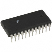
74F673ASPC
N24C
24-Lead Plastic Dual-In-Line Package (PDIP), JEDEC MS-001, 0.300 Wide
Devices also available in Tape and Reel. Specify by appending the suffix letter “X” to the ordering code.
Logic Symbols
IEEE/IEC
Connection Diagram
© 2000 Fairchild Semiconductor Corporation
DS009585
www.fairchildsemi.com
74F673A 16-Bit Serial-In, Serial/Parallel-Out Shift Register
April 1988
�74F673A
Unit Loading/Fan Out
Pin Names
Description
U.L.
Input IIH/IIL
HIGH/LOW
Output IOH/IOL
CS
Chip Select Input (Active LOW)
1.0/1.0
20 µA/−0.6 mA
SHCP
Shift Clock Pulse Input (Active Falling Edge)
1.0/1.0
20 µA/−0.6 mA
STMR
Store Master Reset Input (Active LOW)
1.0/1.0
20 µA/−0.6 mA
STCP
Store Clock Pulse Input
1.0/1.0
20 µA/−0.6 mA
R/W
Read/Write Input
1.0/1.0
20 µA/−0.6 mA
SI/O
Serial Data Input or
3.5/1.0
70 µA/−0.6 mA
3-STATE Serial Output
150/40
−3 mA/24 mA
Parallel Data Outputs
50/33.3
−1 mA/20 mA
Q0–Q15
Functional Description
parallel loading the shift register from the storage register,
serial shifting is inhibited.
The 16-bit shift register operates in one of four modes, as
indicated in the Shift Register Operations Table. A HIGH
signal on the Chip Select (CS) input prevents clocking and
forces the Serial Input/Output (SI/O) 3-STATE buffer into
the high impedance state. During serial shift-out operations, the SI/O buffer is active (i.e., enabled) and the output
data is also recirculated back into the shift register. When
The storage register has an asynchronous master reset
(STMR) input that overrides all other inputs and forces the
Q0–Q15 outputs LOW. The storage register is in the Hold
mode when either CS or the Read/Write (R/W) input is
HIGH. With CS and R/W both LOW, the storage register is
parallel loaded from the shift register.
Shift Register Operations Table
Control Inputs
SI/O
CS R/W SHCP STCP
Status
Storage Register Operations Table
Control Inputs
Operating
Operating Mode
H
X
L
L
L
H
L
H
STMR
CS
R/W
STCP
Mode
X
X
High Z
Hold
L
X
X
X
Reset; Outputs LOW
�
�
X
Data In
Serial Load
H
H
X
X
Hold
L
Data Out Serial Output
H
X
H
H
L
L
�
with Recirculation
H
Active
H = HIGH Voltage Level
L = LOW Voltage Level
X = Immaterial
= LOW-to-HIGH Transition
Parallel Load;
�
No Shifting
H = HIGH Voltage Level
L = LOW Voltage Level
X = Immaterial
= HIGH-to-LOW Transition
�
www.fairchildsemi.com
2
X
Hold
Parallel Load
�74F673A
Block Diagram
3
www.fairchildsemi.com
�74F673A
Absolute Maximum Ratings(Note 1)
Recommended Operating
Conditions
Storage Temperature
−65°C to +150 °C
Ambient Temperature under Bias
−55°C to +125 °C
Free Air Ambient Temperature
Junction Temperature under Bias
−55°C to +150 °C
Supply Voltage
0°C to +70°C
+4.5V to +5.5V
−0.5V to +7.0V
VCC Pin Potential to Ground Pin
Input Voltage (Note 2)
−0.5V to +7.0V
Input Current (Note 2)
−30 mA to +5.0 mA
Voltage Applied to Output
in HIGH State (with VCC = 0V)
Standard Output
−0.5V to VCC
3-STATE Output
−0.5V to +5.5V
Note 1: Absolute maximum ratings are values beyond which the device
may be damaged or have its useful life impaired. Functional operation
under these conditions is not implied.
Note 2: Either voltage limit or current limit is sufficient to protect inputs.
Current Applied to Output
in LOW State (Max)
twice the rated IOL (mA)
DC Electrical Characteristics
Symbol
Parameter
Min
Typ
Max
Input HIGH Voltage
VIL
Input LOW Voltage
0.8
V
VCD
Input Clamp Diode Voltage
−1.2
V
VOH
VOL
IIH
IBVI
2.0
Units
VIH
Conditions
Recognized as a HIGH Signal
Recognized as a LOW Signal
Min
IIN = −18 mA (Non I/O pins)
Output HIGH
10% VCC
2.5
IOH = −1 mA (Qn, SI/O)
Voltage
10% VCC
2.4
IOH = −3 mA (SI/O)
5% VCC
2.7
5% VCC
2.7
V
10% VCC
0.5
Voltage
10% VCC
0.5
Input HIGH Current
Input HIGH Current
Input HIGH Current
Breakdown Test (I/O)
IIL
Input LOW Current
IIH +
Output Leakage
IOZH
Current
IIL +
Output Leakage
IOZL
Current
IOS
Output Short-Circuit Current
ICEX
Output HIGH Leakage Current
Min
IOH = −1 mA (Qn, SI/O)
IOH = −3 mA (SI/O)
Output LOW
Breakdown Test
IBVIT
VCC
V
−60
IOL = 20 mA (Qn)
V
Min
20
µA
Max
VIN = 2.7V (Non I/O pins)
100
µA
Max
VIN = 7.0V (Non I/O pins)
IOL = 24 mA (SI/O)
1.0
mA
Max
VIN = 5.5V (SI/O)
−0.6
mA
Max
VIN = 0.5V
70
µA
Max
VOUT = 2.7V (SI/O)
−650
µA
Max
VOUT = 0.5V (SI/O)
−150
mA
Max
VOUT = 0V
250
µA
Max
VOUT = VCC
IZZ
Bus Drainage Test
500
µA
0.0V
VOUT = 5.25V
ICCH
Power Supply Current
114
172
mA
Max
VO = HIGH
ICCL
Power Supply Current
114
172
mA
Max
VO = LOW
www.fairchildsemi.com
4
�Symbol
Parameter
TA = +25°C
TA = 0°C to +70°C
VCC = +5.0V
VCC = +5.0V
CL = 50 pF
CL = 50 pF
Min
Typ
fMAX
Maximum Clock Frequency
100
130
tPLH
Propagation Delay
3.0
8.0
10.5
2.5
12.0
tPHL
STCP to Qn
3.0
10.5
13.5
2.5
15.0
tPHL
Propagation Delay
6.0
16.5
20.5
5.5
22.5
4.0
6.5
8.5
3.5
9.5
STMR to Qn
Max
Min
Units
Max
85
MHz
tPLH
Propagation Delay
tPHL
SHCP to SI/O
4.5
8.0
10.5
4.0
12.0
tPZH
Output Enable Time
5.0
8.5
11.0
4.0
12.5
tPZL
CS to SI/O
5.5
9.0
11.5
4.5
13.0
tPHZ
Output Disable Time
3.5
5.5
7.5
3.0
8.5
tPLZ
CS to SI/O
3.0
4.5
6.5
2.5
7.5
tPZH
Output Enable Time
4.5
7.5
9.5
4.0
10.5
tPZL
R/W to SI/O
4.5
8.0
10.0
4.0
11.5
tPHZ
Output Disable Time
3.0
5.5
7.0
2.5
8.0
tPLZ
R/W to SI/O
2.5
4.0
5.5
2.0
6.5
ns
ns
ns
ns
ns
AC Operating Requirements
TA = +25°C
Symbol
VCC = +5.0V
Parameter
Min
Max
TA = 0°C to +70°C
VCC = +5.0V
Min
tS(H)
Setup Time, HIGH or LOW
3.5
4.0
tS(L)
CS or R/W to STCP
6.0
7.0
tH(H)
Hold Time, HIGH or LOW
0
0
tH(L)
CS or R/W to STCP
0
0
tS(H)
Setup Time, HIGH or LOW
3.0
3.5
tS(L)
SI/O to SHCP
3.0
3.5
tH(H)
Hold Time, HIGH or LOW
3.0
3.5
tH(L)
SI/O to SHCP
3.0
3.5
5
Units
Max
ns
ns
www.fairchildsemi.com
74F673A
AC Electrical Characteristics
�74F673A
Physical Dimensions inches (millimeters) unless otherwise noted
24-Lead Small Outline Integrated Circuit (SOIC), JEDEC MS-013, 0.300 Wide
Package Number M24B
24-Lead Plastic Dual-In-Line Package (PDIP), JEDEC MS-011, 0.600 Wide
Package Number N24A
www.fairchildsemi.com
6
�74F673A 16-Bit Serial-In, Serial/Parallel-Out Shift Register
Physical Dimensions inches (millimeters) unless otherwise noted (Continued)
24-Lead Plastic Dual-In-Line Package (PDIP), JEDEC MS-001, 0.300 Wide
Package Number N24C
Fairchild does not assume any responsibility for use of any circuitry described, no circuit patent licenses are implied and
Fairchild reserves the right at any time without notice to change said circuitry and specifications.
LIFE SUPPORT POLICY
FAIRCHILD’S PRODUCTS ARE NOT AUTHORIZED FOR USE AS CRITICAL COMPONENTS IN LIFE SUPPORT
DEVICES OR SYSTEMS WITHOUT THE EXPRESS WRITTEN APPROVAL OF THE PRESIDENT OF FAIRCHILD
SEMICONDUCTOR CORPORATION. As used herein:
2. A critical component in any component of a life support
device or system whose failure to perform can be reasonably expected to cause the failure of the life support
device or system, or to affect its safety or effectiveness.
1. Life support devices or systems are devices or systems
which, (a) are intended for surgical implant into the
body, or (b) support or sustain life, and (c) whose failure
to perform when properly used in accordance with
instructions for use provided in the labeling, can be reasonably expected to result in a significant injury to the
user.
www.fairchildsemi.com
7
www.fairchildsemi.com
�
很抱歉,暂时无法提供与“74F673APC”相匹配的价格&库存,您可以联系我们找货
免费人工找货- 国内价格 香港价格
- 15+81.0031715+10.48502