Revised September 2000
74F74
Dual D-Type Positive Edge-Triggered Flip-Flop
General Description
The F74 is a dual D-type flip-flop with Direct Clear and Set
inputs and complementary (Q, Q) outputs. Information at
the input is transferred to the outputs on the positive edge
of the clock pulse. Clock triggering occurs at a voltage level
of the clock pulse and is not directly related to the transition
time of the positive-going pulse. After the Clock Pulse input
threshold voltage has been passed, the Data input is
locked out and information present will not be transferred to
the outputs until the next rising edge of the Clock Pulse
input.
Asynchronous Inputs:
LOW input to SD sets Q to HIGH level
LOW input to CD sets Q to LOW level
Clear and Set are independent of clock
Simultaneous LOW on CD and SD
makes both Q and Q HIGH
Ordering Code:
Order Number
Package Number
Package Description
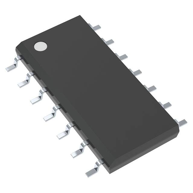
74F74SC
M14A
14-Lead Small Outline Integrated Circuit (SOIC), JEDEC MS-120, 0.150 Narrow
74F74SJ
M14D
14-Lead Small Outline Package (SOP), EIAJ TYPE II, 5.3mm Wide
74F74PC
N14A
14-Lead Plastic Dual-In-Line Package (PDIP), JEDEC MS-001, 0.300 Wide
Devices also available in Tape and Reel. Specify by appending the suffix letter “X” to the ordering code.
Logic Symbols
Connection Diagram
IEEE/IEC
© 2000 Fairchild Semiconductor Corporation
DS009469
www.fairchildsemi.com
74F74 Dual D-Type Positive Edge-Triggered Flip-Flop
April 1988
�74F74
Unit Loading/Fan Out
Pin Names
U.L.
Input IIH/IIL
HIGH/LOW
Output IOH/IOL
20 µA/−0.6 mA
Description
D1 , D2
Data Inputs
1.0/1.0
CP1, CP2
Clock Pulse Inputs (Active Rising Edge)
1.0/1.0
20 µA/−0.6 mA
CD1, CD2
Direct Clear Inputs (Active LOW)
1.0/3.0
20 µA/−1.8 mA
SD1, SD2
Direct Set Inputs (Active LOW)
1.0/3.0
20 µA/−1.8 mA
Q1, Q1, Q2, Q2
Outputs
50/33.3
−1 mA/20 mA
Truth Table
Inputs
Outputs
SD
CD
CP
D
Q
L
H
X
X
H
L
H
L
X
X
L
H
�
�
X
X
H
H
h
H
L
l
L
H
L
X
Q0
Q0
L
L
H
H
H
H
H
H
Q
H (h) = HIGH Voltage Level
L (l) = LOW Voltage Level
X = Immaterial
Q0 = Previous Q (Q) before LOW-to-HIGH Clock Transition
Lower case letters indicate the state of the referenced input or output one setup time prior to the LOW-to-HIGH clock transition.
Logic Diagram
Please note that this diagram is provided only for the understanding of logic operations and should not be used to estimate propagation delays.
www.fairchildsemi.com
2
�74F74
Absolute Maximum Ratings(Note 1)
Recommended Operating
Conditions
Storage Temperature
−65°C to +150°C
Ambient Temperature under Bias
−55°C to +125°C
Free Air Ambient Temperature
Junction Temperature under Bias
−55°C to +150°C
Supply Voltage
0°C to +70°C
+4.5V to +5.5V
−0.5V to +7.0V
VCC Pin Potential to Ground Pin
Input Voltage (Note 2)
−0.5V to +7.0V
Input Current (Note 2)
−30 mA to +5.0 mA
Voltage Applied to Output
in HIGH State (with VCC = 0V)
Standard Output
−0.5V to VCC
3-STATE Output
−0.5V to +5.5V
Note 1: Absolute maximum ratings are values beyond which the device
may be damaged or have its useful life impaired. Functional operation
under these conditions is not implied.
Current Applied to Output
in LOW State (Max)
Note 2: Either voltage limit or current limit is sufficient to protect inputs.
twice the rated IOL (mA)
ESD Last Passing Voltage (Min)
4000V
DC Electrical Characteristics
Symbol
Parameter
Min
Typ
Max
VCC
VIL
Input LOW Voltage
0.8
V
VCD
Input Clamp Diode Voltage
−1.2
V
Min
V
Min
0.5
V
Min
IOL = 20 mA
5.0
µA
Max
VIN = 2.7V
7.0
µA
Max
VIN = 7.0V
50
µA
Max
VOUT = VCC
V
0.0
µA
0.0
mA
Max
−150
mA
Max
16.0
mA
Max
Output HIGH
Voltage
VOL
Output LOW
10% VCC
2.5
5% VCC
2.7
V
Conditions
Input HIGH Voltage
VOH
2.0
Units
VIH
10% VCC
Recognized as a HIGH Signal
Recognized as a LOW Signal
IIN = −18 mA
IOH = −1 mA
IOH = −1 mA
Voltage
IIH
Input HIGH
Current
IBVI
Input HIGH Current
Breakdown Test
ICEX
Output HIGH
Leakage Current
VID
Input Leakage
Test
IOD
4.75
Output Leakage
3.75
Circuit Current
IIL
−0.6
Input LOW Current
−1.8
IOS
Output Short-Circuit Current
ICC
Power Supply Current
−60
10.5
3
IID = 1.9 µA
All Other Pins Grounded
VIOD = 150 mV
All Other Pins Grounded
VIN = 0.5V (D, CP)
VIN = 0.5V (CD, SD)
VOUT = 0V
www.fairchildsemi.com
�74F74
AC Electrical Characteristics
Symbol
Parameter
TA = +25°C
TA = 0°C to +70°C
VCC = +5.0V
VCC = +5.0V
CL = 50 pF
CL = 50 pF
Min
Typ
fMAX
Maximum Clock Frequency
100
125
Max
Min
tPLH
Propagation Delay
3.8
5.3
Max
tPHL
CPn to Qn or Qn
4.4
6.2
8.0
4.4
9.2
tPLH
Propagation Delay
3.2
4.6
6.1
3.2
7.1
tPHL
CDn or SDn to Qn or Qn
3.5
7.0
9.0
3.5
10.5
100
6.8
3.8
Units
MHz
7.8
ns
ns
AC Operating Requirements
TA = +25°C
Symbol
VCC = +5.0V
Parameter
Min
Max
TA = 0°C to +70°C
VCC = +5.0V
Min
tS(H)
Setup Time, HIGH or LOW
2.0
2.0
tS(L)
Dn to CPn
3.0
3.0
tH(H)
Hold Time, HIGH or LOW
1.0
1.0
Units
Max
ns
tH(L)
Dn to CPn
1.0
1.0
tW(H)
CPn Pulse Width
4.0
4.0
tW(L)
HIGH or LOW
5.0
5.0
4.0
4.0
ns
2.0
2.0
ns
tW(L)
CDn or SDn Pulse Width
LOW
tREC
Recovery Time
CDn or SDn to CP
www.fairchildsemi.com
4
ns
�74F74
Physical Dimensions inches (millimeters) unless otherwise noted
14-Lead Small Outline Integrated Circuit (SOIC), JEDEC MS-120, 0.150 Narrow
Package Number M14A
5
www.fairchildsemi.com
�74F74
Physical Dimensions inches (millimeters) unless otherwise noted (Continued)
14-Lead Small Outline Package (SOP), EIAJ TYPE II, 5.3mm Wide
Package Number M14D
www.fairchildsemi.com
6
�74F74 Dual D-Type Positive Edge-Triggered Flip-Flop
Physical Dimensions inches (millimeters) unless otherwise noted (Continued)
14-Lead Plastic Dual-In-Line Package (PDIP), JEDEC MS-001, 0.300 Wide
Package Number N14A
Fairchild does not assume any responsibility for use of any circuitry described, no circuit patent licenses are implied and
Fairchild reserves the right at any time without notice to change said circuitry and specifications.
LIFE SUPPORT POLICY
FAIRCHILD’S PRODUCTS ARE NOT AUTHORIZED FOR USE AS CRITICAL COMPONENTS IN LIFE SUPPORT
DEVICES OR SYSTEMS WITHOUT THE EXPRESS WRITTEN APPROVAL OF THE PRESIDENT OF FAIRCHILD
SEMICONDUCTOR CORPORATION. As used herein:
2. A critical component in any component of a life support
device or system whose failure to perform can be reasonably expected to cause the failure of the life support
device or system, or to affect its safety or effectiveness.
1. Life support devices or systems are devices or systems
which, (a) are intended for surgical implant into the
body, or (b) support or sustain life, and (c) whose failure
to perform when properly used in accordance with
instructions for use provided in the labeling, can be reasonably expected to result in a significant injury to the
user.
www.fairchildsemi.com
7
www.fairchildsemi.com
�
很抱歉,暂时无法提供与“74F74SCX”相匹配的价格&库存,您可以联系我们找货
免费人工找货