Low Voltage Quad 2-Input
OR Gate with 5 V Tolerant
Inputs
74LCX32
The LCX32 contains four 2−input OR gates. The inputs tolerate
voltages up to 7 V allowing the interface of 5 V systems to 3 V
systems.
The 74LCX32 is fabricated with advanced CMOS technology to
achieve high speed operation while maintaining CMOS low power
dissipation.
www.onsemi.com
MARKING DIAGRAM
ON ZXYKK
LCX32
Features
•
•
•
•
•
•
•
•
•
•
5 V Tolerant Inputs
2.3 V – 3.6 V VCC Specifications Provided
5.5 ns tPD Max. (VCC = 3.3 V), 10 mA ICC Max.
Power Down High Impedance Inputs and Outputs
±24 mA Output Drive (VCC = 3.0 V)
Implements Proprietary Noise/EMI Reduction Circuitry
Latch−up Performance Exceeds JEDEC 78 Conditions
ESD performance:
♦ Human Body Model >2000 V
♦ Machine model >150 V
Available on SOIC, TSSOP WB and Leadless QFN Packages
These are Pb−Free Devices
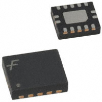
QFN14 3.0x2.5, 0.5P
CASE 510CB
14
ON ZXYKK
LCX32
1
SOIC14
CASE 751EF
14
ON ZXYKK
LCX32
TSSOP−14 WB
CASE 948G
LCX32
Z
XY
KK
1
= Specific Device Code
= Assembly Plant Code
= Date Code
= Lot Run Traceability Code
ORDERING INFORMATION
See detailed ordering and shipping information on page 8 of
this data sheet.
© Semiconductor Components Industries, LLC, 1995
April, 2020 − Rev. 2
1
Publication Order Number:
74LCX32/D
�74LCX32
CONNECTION DIAGRAMS
LOGIC SYMBOL
Figure 3. IEEE/IEC
Figure 1. Pin Assignments for SOIC and TSSOP
PIN DESCRIPTION
Pin Names
An, Bn
On
DAP
Description
Inputs
Outputs
No Connect
1. DAP (Die Attach Pad)
(Top View)
(Bottom View)
Figure 2. Pad Assignments for DQFN
ABSOLUTE MAXIMUM RATINGS
Symbol
VCC
Parameter
Rating
Supply Voltage
–0.5 V to +7.0 V
VI
DC Input Voltage
–0.5 V to +7.0 V
VO
DC Output Voltage, Output in HIGH or LOW State (Note 2)
IIK
DC Input Diode Current, VI < GND
–50 mA
IOK
DC Output Diode Current
VO < GND
–50 mA
VO > VCC
IO
–0.5 V to VCC + 0.5 V
+50 mA
DC Output Source/Sink Current
±50 mA
ICC
DC Supply Current per Supply Pin
±100 mA
IGND
DC Ground Current per Ground Pin
±100 mA
TSTG
Storage Temperature
–65°C to +150°C
Stresses exceeding those listed in the Maximum Ratings table may damage the device. If any of these limits are exceeded, device functionality
should not be assumed, damage may occur and reliability may be affected.
2. IO Absolute Maximum Rating must be observed.
www.onsemi.com
2
�74LCX32
RECOMMENDED OPERATING CONDITIONS (Note 3)
Symbol
VCC
Parameter
Supply Voltage
Operating
Data Retention
Min
Max
Unit
2.0
3.6
V
1.5
3.6
VI
Input Voltage
0
5.5
V
VO
Output Voltage, HIGH or LOW State
0
VCC
V
Output Current
VCC = 3.0 V – 3.6 V
−
±24
mA
VCC = 2.7 V – 3.0 V
−
±12
VCC = 2.3 V – 2.7 V
−
±8
–40
85
°C
0
10
ns/V
IOH / IOL
TA
Dt / DV
Free−Air Operating Temperature
Input Edge Rate, VIN = 0.8 V – 2.0 V, VCC = 3.0 V
Functional operation above the stresses listed in the Recommended Operating Ranges is not implied. Extended exposure to stresses beyond
the Recommended Operating Ranges limits may affect device reliability.
3. Unused inputs must be held HIGH or LOW. They may not float.
DC ELECTRICAL CHARACTERISTICS
−40°C to 85°C
Symbol
VIH
VIL
VOH
VOL
II
Parameter
HIGH Level Input Voltage
LOW Level Input Voltage
HIGH Level Output Voltage
LOW Level Output Voltage
Input Leakage Current
IOFF
Power−Off Leakage Current
ICC
Quiescent Supply Current
DICC
Increase in ICC per Input
Min
Max
Unit
2.3 – 2.7
1.7
−
V
2.7 – 3.6
2.0
−
2.3 – 2.7
−
0.7
2.7 – 3.6
−
0.8
VCC – 0.2
−
VCC (V)
2.3 – 3.6
Conditions
IOH = –100 mA
V
V
2.3
IOH = –8 mA
1.8
−
2.7
IOH = –12 mA
2.2
−
3.0
IOH = –18 mA
2.4
−
IOH = –24 mA
2.2
−
IOL = 100 mA
−
0.2
2.3
IOL = 8 mA
−
0.6
2.7
IOL = 12 mA
−
0.4
3.0
IOL = 16 mA
−
0.4
IOL = 24 mA
−
0.55
0 ≤ VI ≤ 5.5 V
−
±5.0
mA
0
VI or VO = 5.5 V
−
10
mA
2.3 – 3.6
VI = VCC or GND
−
10
mA
3.6 V ≤ VI ≤ 5.5 V
−
±10
VIH = VCC – 0.6 V
−
500
2.3 – 3.6
2.3 – 3.6
2.3 – 3.6
www.onsemi.com
3
V
mA
�74LCX32
AC ELECTRICAL CHARACTERISTICS
TA = –40�C to +85�C, RL = 500 W
VCC = 3.3 V + 0.3 V,
CL = 50 pF
Symbol
Parameter
Propagation Delay
tPHL, tPLH
tOSHL, tOSLH
Output to Output Skew (Note 4)
VCC = 2.7 V,
CL = 50 pF
VCC = 2.5 V + 0.2 V,
CL = 30 pF
Min
Max
Min
Max
Min
Max
Unit
1.5
5.5
1.5
6.2
1.5
6.6
ns
−
1.0
−
−
−
−
ns
4. Skew is defined as the absolute value of the difference between the actual propagation delay for any two separate outputs of the same device.
The specification applies to any outputs switching in the same direction, either HIGH−to−LOW (tOSHL) or LOW−to−HIGH (tOSLH).
DYNAMIC SWITCHING CHARACTERISTICS
TA = 25°C
Symbol
VOLP
VOLV
Parameter
Quiet Output Dynamic Peak VOL
Quiet Output Dynamic Valley VOL
VCC (V)
Conditions
Typical
Unit
V
3.3
CL = 50 pF, VIH = 3.3 V, VIL = 0 V
0.8
2.5
CL = 30 pF, VIH = 2.5 V, VIL = 0 V
0.6
3.3
CL = 50 pF, VIH = 3.3 V, VIL = 0 V
–0.8
2.5
CL = 30 pF, VIH = 2.5 V, VIL = 0 V
–0.6
V
CAPACITANCE
Symbol
CIN
Parameter
Conditions
Typical
Input Capacitance
VCC = Open, VI = 0 V or VCC
7
pF
COUT
Output Capacitance
VCC = 3.3 V, VI = 0 V or VCC
8
pF
CPD
Power Dissipation Capacitance
VCC = 3. 3 V, VI = 0 V or VCC, f = 10 MHz
25
pF
www.onsemi.com
4
�74LCX32
AC LOADING AND WAVEFORMS (GENERIC FOR LCX FAMILY)
Test
Switch
tPLH, tPHL
Open
tPZL, tPLZ
6 V at VCC = 3.3 ± 0.3 V
VCC x 2 at VCC = 2.5 ± 0.2 V
tPZH, tPHZ
GND
Figure 4. AC Test Circuit (CL Includes Probe and Jig Capacitance)
Waveform for Inverting and Non−Inverting Functions
3−STATE Output Low Enable and Disable Times for Logic
Propagation Delay. Pulse Width and trec Waveforms
Setup Time, Hold Time and Recovery Time for Logic
3−STATE Output High Enable and Disable Times for Logic
trise and tfall
VCC
Symbol
3.3 V � 0.3 V
2.7 V
Vmi
1.5 V
1.5 V
2.5 V � 0.2 V
CC / 2
Vmo
1.5 V
1.5 V
CC / 2
Vx
V OL + 0.3 V
V OL + 0.3 V
VOL + 0.15 V
Vy
V OH – 0.3 V
V OH – 0.3 V
VOH – 0.15 V
Figure 5. Waveforms (Input Characteristics; f = 1 MHz, tr = tf = 3 ns)
www.onsemi.com
5
�74LCX32
SCHEMATIC DIAGRAM (GENERIC FOR LCX FAMILY)
Figure 6. Schematic Diagram (Generic for LCX Family)
www.onsemi.com
6
�74LCX32
TAPE AND REEL SPECIFICATION
Tape Format for DQFN
TAPE FORMAT FOR DQFN
Package Designator
Tape Section
Number of Cavities
Cavity Status
Cover Tape Status
BQX
Leader (Start End)
125 (Typ.)
Empty
Sealed
Carrier
3000
Filled
Sealed
Trailer (Hub End)
75 (Typ.)
Empty
Sealed
Tape Dimensions (Inches (Millimeters))
Figure 7. Tape Dimensions (Inches (Millimeters))
www.onsemi.com
7
�74LCX32
Reel Dimensions (Inches (Millimeters))
Figure 8.
Tape Size
A
B
C
D
N
W1
W2
12 mm
13.0 (330.0)
0.059 (1.50)
0.512 (13.00)
0.795 (20.20)
2.165 (55.00)
0.488 (12.4)
0.724 (18.4)
ORDERING INFORMATION
Package Number
Package Description
Shipping†
74LCX32M
SOIC14
14−Lead Small Outline Integrated Circuit (SOIC),
JEDEC MS−012, 0.150” Narrow
1100 Units / Tube
74LCX32BQX
(Note 5)
QFN14
14−Terminal Depopulated Quad Very−Thin Flat Pack
No Leads (DQFN), JEDEC MO−241, 2.5 x 3.0 mm
3000 Units / Tape & Reel
74LCX32MTC
TSSOP−14 WB
14−Lead Thin Shrink Small Outline Package (TSSOP),
JEDEC MO−153, 4.4 mm Wide
2350 Units / Tube
74LCX32MTCX
TSSOP−14 WB
14−Lead Thin Shrink Small Outline Package (TSSOP),
JEDEC MO−153, 4.4 mm Wide
2500 Units / Tape & Reel
Ordering Number
†For information on tape and reel specifications, including part orientation and tape sizes, please refer to our Tape and Reel Packaging
Specifications Brochure, BRD8011/D.
5. DQFN package available in Tape and Reel only.
6. Device also available in Tape and Reel. Specify by appending suffix letter “X” to the ordering number.
7. All packages are lead free per JEDEC: J−STD−020B standard.
www.onsemi.com
8
�MECHANICAL CASE OUTLINE
PACKAGE DIMENSIONS
QFN14 3.0x2.5, 0.5P
CASE 510CB
ISSUE O
0.05 C
3.00
DATE 31 AUG 2016
4.00 MAX
2.20 MAX
1.40 MAX
B
A
2X
1.00
MAX
2.50
1.70
MAX
0.50 TYP
3.50
MAX
PIN #1 QUADRANT
0.05 C
TOP VIEW
(0.90)
2X
0.50 TYP
0.24 TYP
RECOMMENDED LAND PATTERN
0.80±0.05
0.10 C
0.20±0.05
0.08 C
0.025±0.025
SEATING
PLANE
C
SIDE VIEW
3.00±0.05
1.65±0.05
PIN #1 IDENT
0.370±0.05
(14X)
A. CONFORMS TO JEDEC REGISTRATION
MO−241, VARIATION AA
B. DIMENSIONS ARE IN MILLIMETERS.
0.50
2.00
0.25±0.05
(14X)
BOTTOM VIEW
DOCUMENT NUMBER:
DESCRIPTION:
C. DIMENSIONS AND TOLERANCES PER
ASME Y14.5M, 2009.
1.15±0.05
2.50±0.05
0.50
98AON13643G
QFN14 3.0X2.5, 0.5P
0.10
0.05
D. LAND PATTERN RECOMMENDATION IS
EXISTING INDUSTRY LAND PATTERN.
C A B
C
Electronic versions are uncontrolled except when accessed directly from the Document Repository.
Printed versions are uncontrolled except when stamped “CONTROLLED COPY” in red.
PAGE 1 OF 1
ON Semiconductor and
are trademarks of Semiconductor Components Industries, LLC dba ON Semiconductor or its subsidiaries in the United States and/or other countries.
ON Semiconductor reserves the right to make changes without further notice to any products herein. ON Semiconductor makes no warranty, representation or guarantee regarding
the suitability of its products for any particular purpose, nor does ON Semiconductor assume any liability arising out of the application or use of any product or circuit, and specifically
disclaims any and all liability, including without limitation special, consequential or incidental damages. ON Semiconductor does not convey any license under its patent rights nor the
rights of others.
© Semiconductor Components Industries, LLC, 2019
www.onsemi.com
�MECHANICAL CASE OUTLINE
PACKAGE DIMENSIONS
SOIC14
CASE 751EF
ISSUE O
DOCUMENT NUMBER:
DESCRIPTION:
98AON13739G
SOIC14
DATE 30 SEP 2016
Electronic versions are uncontrolled except when accessed directly from the Document Repository.
Printed versions are uncontrolled except when stamped “CONTROLLED COPY” in red.
PAGE 1 OF 1
ON Semiconductor and
are trademarks of Semiconductor Components Industries, LLC dba ON Semiconductor or its subsidiaries in the United States and/or other countries.
ON Semiconductor reserves the right to make changes without further notice to any products herein. ON Semiconductor makes no warranty, representation or guarantee regarding
the suitability of its products for any particular purpose, nor does ON Semiconductor assume any liability arising out of the application or use of any product or circuit, and specifically
disclaims any and all liability, including without limitation special, consequential or incidental damages. ON Semiconductor does not convey any license under its patent rights nor the
rights of others.
© Semiconductor Components Industries, LLC, 2019
www.onsemi.com
�MECHANICAL CASE OUTLINE
PACKAGE DIMENSIONS
TSSOP−14 WB
CASE 948G
ISSUE C
14
DATE 17 FEB 2016
1
SCALE 2:1
14X K REF
0.10 (0.004)
0.15 (0.006) T U
M
T U
V
S
S
S
N
2X
14
L/2
0.25 (0.010)
8
M
B
−U−
L
PIN 1
IDENT.
N
F
7
1
0.15 (0.006) T U
NOTES:
1. DIMENSIONING AND TOLERANCING PER
ANSI Y14.5M, 1982.
2. CONTROLLING DIMENSION: MILLIMETER.
3. DIMENSION A DOES NOT INCLUDE MOLD
FLASH, PROTRUSIONS OR GATE BURRS.
MOLD FLASH OR GATE BURRS SHALL NOT
EXCEED 0.15 (0.006) PER SIDE.
4. DIMENSION B DOES NOT INCLUDE
INTERLEAD FLASH OR PROTRUSION.
INTERLEAD FLASH OR PROTRUSION SHALL
NOT EXCEED 0.25 (0.010) PER SIDE.
5. DIMENSION K DOES NOT INCLUDE DAMBAR
PROTRUSION. ALLOWABLE DAMBAR
PROTRUSION SHALL BE 0.08 (0.003) TOTAL
IN EXCESS OF THE K DIMENSION AT
MAXIMUM MATERIAL CONDITION.
6. TERMINAL NUMBERS ARE SHOWN FOR
REFERENCE ONLY.
7. DIMENSION A AND B ARE TO BE
DETERMINED AT DATUM PLANE −W−.
S
DETAIL E
K
A
−V−
K1
J J1
ÉÉÉ
ÇÇÇ
ÇÇÇ
ÉÉÉ
SECTION N−N
−W−
C
0.10 (0.004)
−T− SEATING
PLANE
H
G
D
DETAIL E
DIM
A
B
C
D
F
G
H
J
J1
K
K1
L
M
MILLIMETERS
INCHES
MIN
MAX
MIN MAX
4.90
5.10 0.193 0.200
4.30
4.50 0.169 0.177
−−−
1.20
−−− 0.047
0.05
0.15 0.002 0.006
0.50
0.75 0.020 0.030
0.65 BSC
0.026 BSC
0.50
0.60 0.020 0.024
0.09
0.20 0.004 0.008
0.09
0.16 0.004 0.006
0.19
0.30 0.007 0.012
0.19
0.25 0.007 0.010
6.40 BSC
0.252 BSC
0_
8_
0_
8_
GENERIC
MARKING DIAGRAM*
14
SOLDERING FOOTPRINT
XXXX
XXXX
ALYWG
G
7.06
1
1
0.65
PITCH
14X
0.36
14X
1.26
DIMENSIONS: MILLIMETERS
DOCUMENT NUMBER:
98ASH70246A
DESCRIPTION:
TSSOP−14 WB
A
L
Y
W
G
= Assembly Location
= Wafer Lot
= Year
= Work Week
= Pb−Free Package
(Note: Microdot may be in either location)
*This information is generic. Please refer to
device data sheet for actual part marking.
Pb−Free indicator, “G” or microdot “G”, may
or may not be present. Some products may
not follow the Generic Marking.
Electronic versions are uncontrolled except when accessed directly from the Document Repository.
Printed versions are uncontrolled except when stamped “CONTROLLED COPY” in red.
PAGE 1 OF 1
onsemi and
are trademarks of Semiconductor Components Industries, LLC dba onsemi or its subsidiaries in the United States and/or other countries. onsemi reserves
the right to make changes without further notice to any products herein. onsemi makes no warranty, representation or guarantee regarding the suitability of its products for any particular
purpose, nor does onsemi assume any liability arising out of the application or use of any product or circuit, and specifically disclaims any and all liability, including without limitation
special, consequential or incidental damages. onsemi does not convey any license under its patent rights nor the rights of others.
© Semiconductor Components Industries, LLC, 2019
www.onsemi.com
�onsemi,
, and other names, marks, and brands are registered and/or common law trademarks of Semiconductor Components Industries, LLC dba “onsemi” or its affiliates
and/or subsidiaries in the United States and/or other countries. onsemi owns the rights to a number of patents, trademarks, copyrights, trade secrets, and other intellectual property.
A listing of onsemi’s product/patent coverage may be accessed at www.onsemi.com/site/pdf/Patent−Marking.pdf. onsemi reserves the right to make changes at any time to any
products or information herein, without notice. The information herein is provided “as−is” and onsemi makes no warranty, representation or guarantee regarding the accuracy of the
information, product features, availability, functionality, or suitability of its products for any particular purpose, nor does onsemi assume any liability arising out of the application or use
of any product or circuit, and specifically disclaims any and all liability, including without limitation special, consequential or incidental damages. Buyer is responsible for its products
and applications using onsemi products, including compliance with all laws, regulations and safety requirements or standards, regardless of any support or applications information
provided by onsemi. “Typical” parameters which may be provided in onsemi data sheets and/or specifications can and do vary in different applications and actual performance may
vary over time. All operating parameters, including “Typicals” must be validated for each customer application by customer’s technical experts. onsemi does not convey any license
under any of its intellectual property rights nor the rights of others. onsemi products are not designed, intended, or authorized for use as a critical component in life support systems
or any FDA Class 3 medical devices or medical devices with a same or similar classification in a foreign jurisdiction or any devices intended for implantation in the human body. Should
Buyer purchase or use onsemi products for any such unintended or unauthorized application, Buyer shall indemnify and hold onsemi and its officers, employees, subsidiaries, affiliates,
and distributors harmless against all claims, costs, damages, and expenses, and reasonable attorney fees arising out of, directly or indirectly, any claim of personal injury or death
associated with such unintended or unauthorized use, even if such claim alleges that onsemi was negligent regarding the design or manufacture of the part. onsemi is an Equal
Opportunity/Affirmative Action Employer. This literature is subject to all applicable copyright laws and is not for resale in any manner.
PUBLICATION ORDERING INFORMATION
LITERATURE FULFILLMENT:
Email Requests to: orderlit@onsemi.com
onsemi Website: www.onsemi.com
◊
TECHNICAL SUPPORT
North American Technical Support:
Voice Mail: 1 800−282−9855 Toll Free USA/Canada
Phone: 011 421 33 790 2910
Europe, Middle East and Africa Technical Support:
Phone: 00421 33 790 2910
For additional information, please contact your local Sales Representative
�


 工商网监
湘ICP备2023018690号
工商网监
湘ICP备2023018690号