Revised April 2005
74LVX573
Low Voltage Octal Latch with 3-STATE Outputs
General Description
Features
The LVX573 is a high-speed octal latch with buffered common Latch Enable (LE) and buffered common Output
Enable (OE) inputs. The LVX573 is functionally identical to
the LVX373 but with inputs and outputs on opposite sides
of the package. The inputs tolerate up to 7V allowing interface of 5V systems to 3V systems.
■ Input voltage translation from 5V to 3V
■ Ideal for low power/low noise 3.3V applications
■ Guaranteed simultaneous switching noise level and
dynamic threshold performance
Ordering Code:
Order Number
74LVX573M
74LVX573SJ
74LVX573MTC
Package Number
Package Description
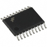
M20B
20-Lead Small Outline Integrated Circuit (SOIC), JEDEC MS-013, 0.300" Wide
M20D
Pb-Free 20-Lead Small Outline Package (SOP), EIAJ TYPE II, 5.3mm Wide
MTC20
20-Lead Thin Shrink Small Outline Package (TSSOP), JEDEC MO-153, 4.4mm Wide
Devices also available in Tape and Reel. Specify by appending suffix letter “X” to the ordering code.
Pb-Free package per JEDEC J-STD-020B.
Logic Symbols
Connection Diagram
IEEE/IEC
Pin Descriptions
Pin Names
© 2005 Fairchild Semiconductor Corporation
DS011616
Description
D0–D7
Data Inputs
LE
Latch Enable Input
OE
3-STATE Output Enable Input
O0–O7
3-STATE Latch Outputs
www.fairchildsemi.com
74LVX573 Low Voltage Octal Latch with 3-STATE Outputs
June 1993
�74LVX573
Functional Description
Truth Table
The LVX573 contains eight D-type latches. When the
enable (LE) input is HIGH, data on the Dn inputs enters the
latches. In this condition the latches are transparent, i.e., a
latch output will change state each time its D input
changes. When LE is LOW the latches store the information that was present on the D inputs a setup time preceding the HIGH-to-LOW transition of LE. The 3-STATE
buffers are controlled by the Output Enable (OE) input.
When OE is LOW, the buffers are enabled. When OE is
HIGH the buffers are in the high impedance mode but this
does not interfere with entering new data into the latches.
Inputs
H
L
Z
X
O0
Outputs
OE
LE
D
On
L
H
H
H
L
H
L
L
L
L
X
O0
H
X
X
Z
HIGH Voltage
LOW Voltage
High Impedance
Immaterial
Previous O0 before HIGH-to-LOW transition of Latch Enable
Logic Diagram
Please note that this diagram is provided only for the understanding of logic operations and should not be used to estimate propagation delays.
www.fairchildsemi.com
2
�Recommended Operating
Conditions (Note 2)
�0.5V to �7.0V
Supply Voltage (VCC)
DC Input Diode Current (IIK)
VI
Supply Voltage (VCC)
�0.5V
�20 mA
�0.5V to 7V
DC Input Voltage (VI)
VO
0V to 5.5V
Output Voltage (VO)
DC Output Diode Current (IOK)
VO
2.0V to 3.6V
Input Voltage (VI)
0V to VCC
�40qC to �85qC
Operating Temperature (TA)
�0.5V
VCC � 0.5V
�20 mA
�20 mA
�0.5V to VCC � 0.5V
DC Output Voltage (VO)
Input Rise and Fall Time ('t/'V)
Note 1: The “Absolute Maximum Ratings” are those values beyond which
the safety of the device cannot be guaranteed. The device should not be
operated at these limits. The parametric values defined in the Electrical
Characteristics tables are not guaranteed at the absolute maximum ratings.
The “Recommended Operating Conditions” table will define the conditions
for actual device operation.
DC Output Source
r25 mA
or Sink Current (IO)
DC VCC or Ground Current
r75 mA
�65qC to �150qC
(ICC or IGND)
Storage Temperature (TSTG)
Power Dissipation
0 ns/V to 100 ns/V
Note 2: Unused inputs must be held HIGH or LOW. They may not float.
180 mW
DC Electrical Characteristics
Symbol
VIH
VIL
VOH
VOL
IOZ
Parameter
VCC
TA
Min
�25qC
TA
Typ
Max
�40qC to �85qC
Min
HIGH Level
2.0
1.5
1.5
Input Voltage
3.0
2.0
2.0
3.6
2.4
2.4
2.0
0.5
0.5
Input Voltage
3.0
0.8
0.8
3.6
0.8
0.8
2.0
1.9
2.0
1.9
Output Voltage
3.0
2.9
3.0
2.9
3.0
2.58
V
VIN
VIH or VIL IOH
�50 PA
IOH
�50 PA
V
2.48
LOW Level
2.0
0.0
Output Voltage
3.0
0.0
3-STATE Output
Conditions
V
LOW Level
HIGH Level
Units
Max
IOH
0.1
0.1
VIN
0.1
0.1
3.0
0.36
0.44
3.6
r0.25
r2.5
PA
VIN
50 PA
IOL
50 PA
IOL
4 mA
V
Off-State Current
�4 mA
VIH or VIL IOL
VIH or VIL
VOUT
VCC or GND
IIN
Input Leakage Current
3.6
r0.1
r1.0
PA
VIN
5.5V or GND
ICC
Quiescent Supply Current
3.6
4.0
40.0
PA
VIN
VCC or GND
Noise Characteristics (Note 3)
Symbol
VCC
Parameter
(V)
TA
Typ
25qC
Units
CL (pF)
50
Limit
VOLP
Quiet Output Maximum Dynamic VOL
3.3
0.5
0.8
V
VOLV
Quiet Output Minimum Dynamic VOL
3.3
�0.5
�0.8
V
50
VIHD
Minimum HIGH Level Dynamic Input Voltage
3.3
2.0
V
50
VILD
Maximum LOW Level Dynamic Input Voltage
3.3
0.8
V
50
Note 3: (Input tr
tf
3ns)
3
www.fairchildsemi.com
74LVX573
Absolute Maximum Ratings(Note 1)
�74LVX573
AC Electrical Characteristics
Symbol
Parameter
tPLH
Propagation
tPHL
Delay Time
Dn to On
tPLH
Propagation
tPHL
Delay Time
LE to On
tPZL
3-STATE Output
tPZH
Enable Time
VCC
(V)
2.7
3-STATE Output
tPHZ
Disable Time
tW
LE Pulse
Width
tS
Setup Time
Dn to LE
tH
Hold Time
Dn to LE
TA
�40qC to �85qC
Typ
Max
Min
Max
7.6
14.5
1.0
17.5
10.1
18.0
1.0
21.0
5.9
9.3
1.0
11.0
8.4
12.8
1.0
8.2
15.6
10.7
Units
Conditions
CL
15 pF
CL
50 pF
CL
15 pF
14.5
CL
50 pF
1.0
18.5
CL
15 pF
19.1
1.0
22.0
CL
50 pF
6.4
10.1
1.0
12.0
CL
15 pF
8.9
13.6
1.0
15.5
CL
50 pF
7.8
15.0
1.0
18.5
CL
15 pF, RL
1 k:
10.3
18.5
1.0
22.0
CL
50 pF, RL
1 k:
6.1
9.7
1.0
12.0
CL
15 pF, RL
1 k:
8.6
13.2
1.0
15.5
CL
50 pF, RL
1 k:
2.7
12.1
19.1
1.0
22.0
CL
50 pF, RL
1 k:
3.3 r 0.3
10.1
13.6
1.0
15.5
CL
50 pF, RL
1 k:
CL
50 pF
3.3 r 0.3
2.7
3.3 r 0.3
2.7
3.3 r 0.3
tPLZ
�25qC
TA
Min
2.7
6.5
5.0
5.0
2.7
5.0
5.0
3.3 r 0.3
3.5
3.5
2.7
1.5
1.5
ns
ns
3.3 r 0.3
1.5
ns
ns
ns
1.5
tOSHL
Output to Output
2.7
1.5
1.5
tOSLH
Skew (Note 4)
2.3
1.5
1.5
|tPLHm � tPLHn|, tOSHL
ns
7.5
3.3 r 0.3
Note 4: Parameter guaranteed by design. tOSLH
ns
ns
|tPHLm � tPHLn|.
Capacitance
Symbol
TA
Parameter
Min
�25qC
TA
Typ
Max
10
�40qC to �85qC
Min
Max
10
Units
CIN
Input Capacitance
4
COUT
Output Capacitance
6
pF
CPD
Power Dissipation
27
pF
Capacitance (Note 5)
Note 5: CPD is defined as the value of the internal equivalent capacitance which is calculated from the operating current consumption without load.
www.fairchildsemi.com
4
pF
�74LVX573
Physical Dimensions inches (millimeters) unless otherwise noted
20-Lead Small Outline Integrated Circuit (SOIC), JEDEC MS-013, 0.300" Wide
Package Number M20B
5
www.fairchildsemi.com
�74LVX573
Physical Dimensions inches (millimeters) unless otherwise noted (Continued)
Pb-Free 20-Lead Small Outline Package (SOP), EIAJ TYPE II, 5.3mm Wide
Package Number M20D
www.fairchildsemi.com
6
�74LVX573 Low Voltage Octal Latch with 3-STATE Outputs
Physical Dimensions inches (millimeters) unless otherwise noted (Continued)
20-Lead Thin Shrink Small Outline Package (TSSOP), JEDEC MO-153, 4.4mm Wide
Package Number MTC20
Fairchild does not assume any responsibility for use of any circuitry described, no circuit patent licenses are implied and
Fairchild reserves the right at any time without notice to change said circuitry and specifications.
LIFE SUPPORT POLICY
FAIRCHILD’S PRODUCTS ARE NOT AUTHORIZED FOR USE AS CRITICAL COMPONENTS IN LIFE SUPPORT
DEVICES OR SYSTEMS WITHOUT THE EXPRESS WRITTEN APPROVAL OF THE PRESIDENT OF FAIRCHILD
SEMICONDUCTOR CORPORATION. As used herein:
2. A critical component in any component of a life support
device or system whose failure to perform can be reasonably expected to cause the failure of the life support
device or system, or to affect its safety or effectiveness.
1. Life support devices or systems are devices or systems
which, (a) are intended for surgical implant into the
body, or (b) support or sustain life, and (c) whose failure
to perform when properly used in accordance with
instructions for use provided in the labeling, can be reasonably expected to result in a significant injury to the
user.
www.fairchildsemi.com
7
www.fairchildsemi.com
�
很抱歉,暂时无法提供与“74LVX573MTCX”相匹配的价格&库存,您可以联系我们找货
免费人工找货- 国内价格 香港价格
- 2500+3.096852500+0.40115
- 国内价格 香港价格
- 2500+3.280412500+0.42493
- 5000+3.196265000+0.41403